Proceeding Paper

Post Fabrication Processing of Foundry MEMS Structures Exhibiting Large, Out-of-Plane Deflections †

1
Sensors Directorate, Air Force Research Laboratory, Wright-Patterson AFB, OH 45433, USA
2
Air Force Institute of Technology, Wright-Patterson AFB, OH 45433, USA
*
Author to whom correspondence should be addressed.
Presented at the Eurosensors 2017 Conference, Paris, France, 3–6 September 2017.
Proceedings 2017, 1(4), 553; https://doi.org/10.3390/proceedings1040553
Published: 18 August 2017
(This article belongs to the Proceedings of Proceedings of Eurosensors 2017, Paris, France, 3–6 September 2017)

Abstract

:
This research effort is focused on the development of large angle, out-of-plane bimorph MEMS micromirrors fabricated in the PolyMUMPs foundry process. Based on design constraints of the PolyMUMPs process, current designs fabricated do not meet the requirements to enable large angle optical steering. Through Comsol modeling and simulation, several post-processing techniques were discovered that could be used to meet the required large out-of-plane deflections. We have performed several post-processing techniques to include silicon nitride and high temperature evaporated gold to verify our Comsol modeling results. Our experimental tests validate the Comsol results of greater than 400 µm deflections are achievable.

1. Introduction

Current Micro-Electro-Mechanical system (MEMS) designers have few options when it comes to commercial foundries in the fabrication of microsystems. In general, MEMS designers are limited to the materials and design rules established by the foundry. Large angle beamsteering is highly desired in many applications for example in the medical imaging area of endoscopy [1,2]; however, meeting the steering angle requirements of 20–35° is extremely difficult, especially within a constrained surface area and bias voltage limitations. Several different actuation assemblies were fabricated in the PolyMUMPs fabrication process; however, they did not meet the out-of-plane upward deflections necessary to enable large angle tip, tilt, and piston motion. Thus, several post-processing techniques were used to enhance the out-of-plane deflections of the actuation assemblies to enable large optical beam steering.

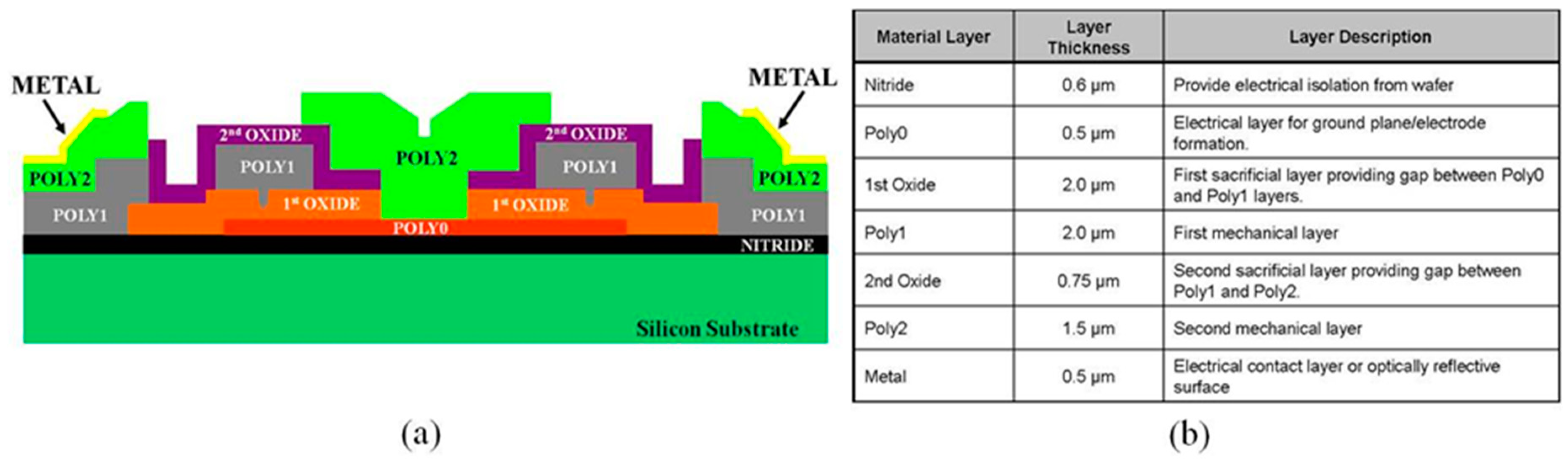
2. PolyMUMPs Foundry Fabrication Process

The foundation of the design uses the PolyMUMPs fabrication process which is outlined in [3] with Figure 1a illustrating a cross sectional view of all deposition layers and Figure 1b outlining each layer thickness and layer functionality. The surface material layers are deposited by low pressure chemical vapor deposition (LPCVD). The sacrificial oxide layers, which consist of phosphosilicate glass (PSG) serve two purposes: (1) defines the gaps between structural layers, and (2) serves as the dopant source for the 1050 °C high temperature phosphorus diffusions to reduce the resistivity in the polysilicon structural layers. All surface layers are patterned using standard photolithography techniques and etched using Reactive Ion Etching (RIE). The final surface layer, a 0.5 μm-thick gold metallization layer with a 100 nm chrome adhesion layer is deposited and patterned using a standard lift-off technique. Lastly, a release etch is performed to remove the sacrificial oxide layers freeing the structural polysilicon layers (Poly1 and Poly2). The typical release etch is performed by immersing the die in room temperature hydrofluoric (49%) acid for 2–3 min, methanol rinses to stop the HF etch, and then a supercritical carbon dioxide (CO2) rapid dry to minimize stiction of the actuation assemblies.

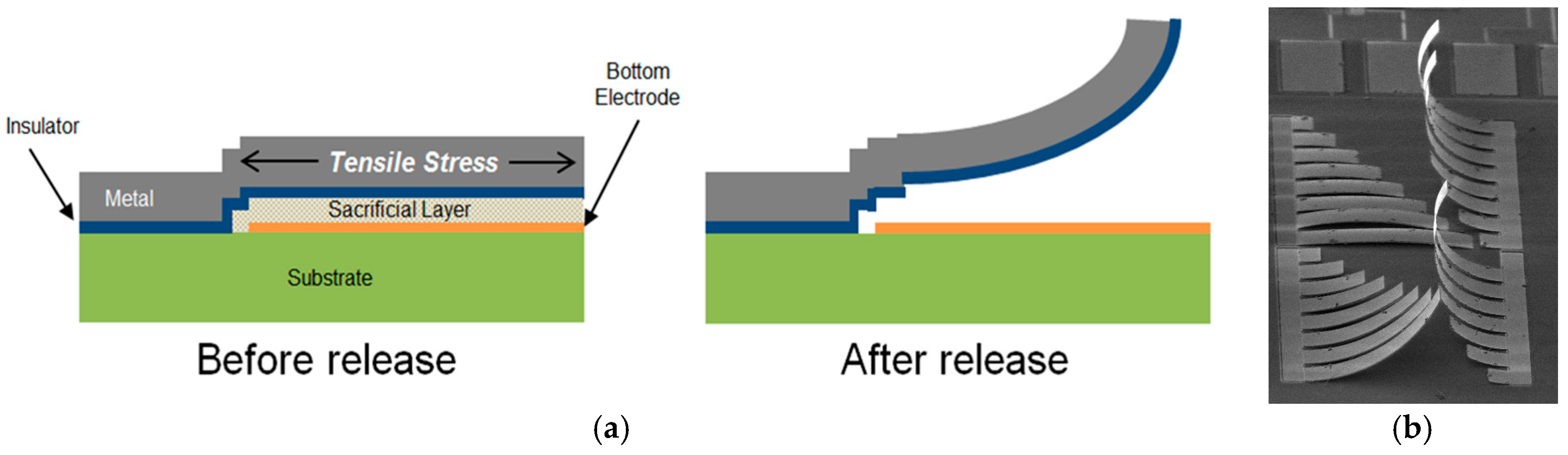
3. Design Methodology

As shown in Figure 1 above, to maximize the out-of-plane deflections, we strictly used the Poly2 and gold layers to create the bimorph beam structures of the actuation assembly. The actuator design concept capitalizes on the residual stress and the coefficient of thermal expansion (CTE) differences between the two layers. The concept is shown in Figure 2 below where the left image in Figure 2a illustrates the as designed layers and the right image of Figure 2a shows the same design following the removal of the sacrificial layer. Figure 2b illustrates and scanning electron microscope (SEM) image of the design concept as fabricated in the PolyMUMPs foundry process. In addition, as shown in Figure 2a, the Poly0 layer is used to create the fixed, lower electrode for all electrostatic designs as well as to provide the necessary wiring of the electrodes to select bond pads for testing.

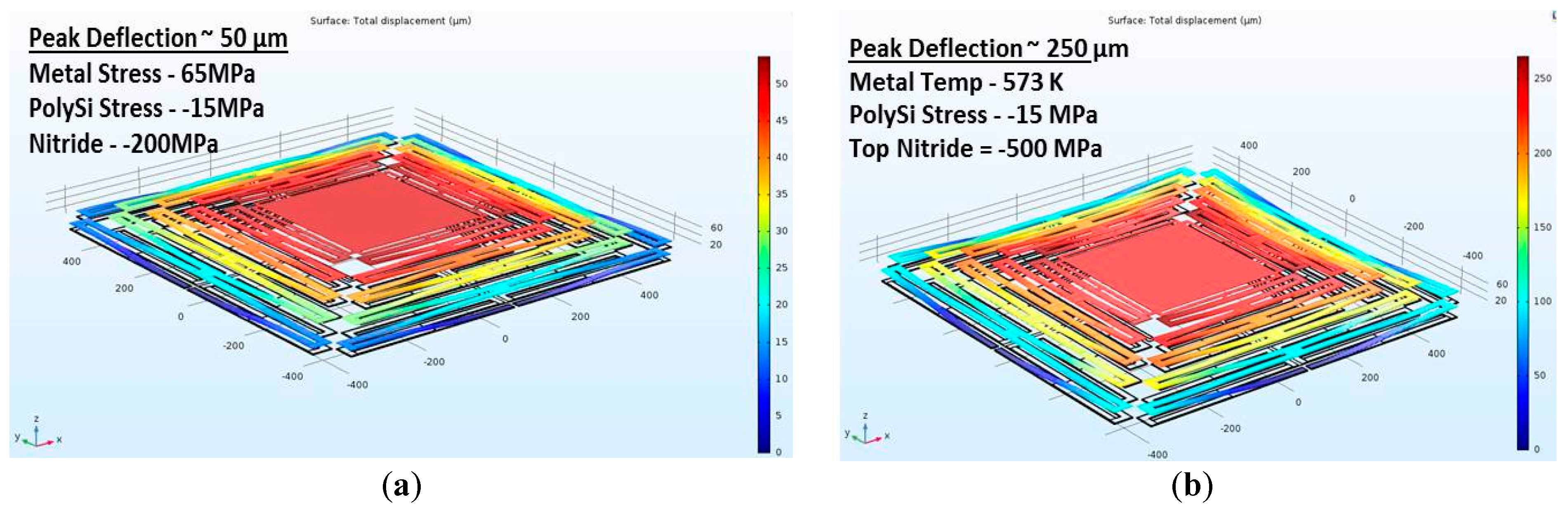
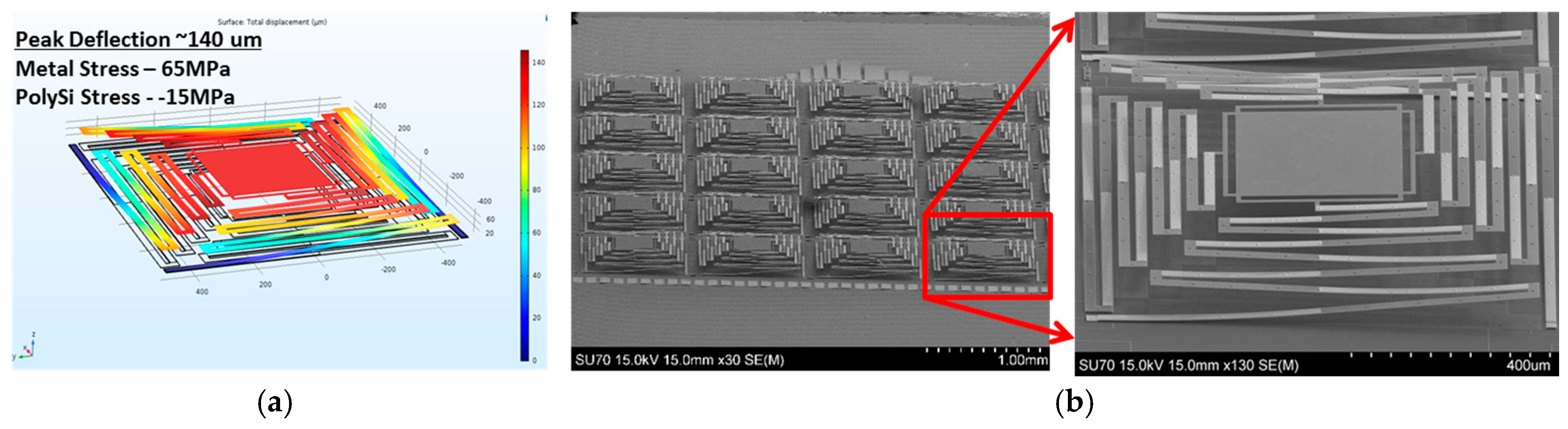
4. Electrothermal Actuator Modeling Using Comsol FEM and Experimental Results

Comsol finite element modeling (FEM) software was used to model the pre and post-processed foundry fabricated MEMS designs to determine the out-of-plane deflections. Based on the design constraints of the foundry process and our allotted design space criteria for a single element (1 mm2), the PolyMUMPs foundry does not meet the required deflections as shown in the SEM image in Figure 3a. From this SEM image and the corresponding Comsol simulation shown in Figure 3b of the structure, both show an overall peak deflection of zero microns. This is due to the full bimorph beams lacking a bending moment component which can force the beam tips to deflect downward, creating an elongated ‘S’ shaped final profile. In the current PolyMUMPs foundry fabrication, there are no additional material layers available which can be used to create this bending moment.
As illustrated in Figure 3 both images illustrate the bimorph beams upward bending which when coupled with a silicon nitride (SiN) deposition placed on top of the gold/polysilicon stacked beams, can indeed create the necessary bending moment to cause the actuation assembly to deflect upward as shown in Figure 4. Therefore, through the use of the PolyMUMPs structural layers as the foundation of the actuation assembly, post processing depositions of SiN (Figure 4a) and high temperature gold metal evaporation (up to 300 °C) (Figure 4b) can be used to achieve the upward deflections needed for large angle beam steering. Figure 4a) illustrates the as fabricated PolyMUMPs electrothermal design with a SiN layer deposited by plasma enhanced chemical vapor deposition (PECVD) at a stress level of −200 MPa at 300 °C shows a deflection of ~50 µm. In Figure 4b, the PolyMUMPs gold layer was removed and replaced with a gold layer deposited at 300 °C. A −500 MPa PECVD SiN layer was then deposited at 300 °C. As shown, over 250 µm can be achieved using these post-processing techniques. The electrothermal PolyMUMPs design provided an out-of-plane deflection of 162 ± 5 µm using a coupled SiN layer exhibiting a stress level of −930 MPa. All deflections are determined using white light interferometry (IFM).

5. Electrostatic Actuator Modeling and Experimental Results

The post-processing steps outlined above were repeated for an electrostatically actuated design utilizing a beam structure in the form of a folded cantilever beam or serpentine layout [4]. The baseline electrostatic design fabricated in the PolyMUMPs fabrication process resulted in an out-of-plane deflection of ~140 µm as shown in the Comsol image in Figure 5a,b illustrates a 5 × 4 array of these structures with a close up view shown on the right of a single actuation assembly. The out-of-plane deflection was measured to be ~148 µm using an IFM. This deflection does not meet the out-of-plane deflections required for large angle beam steering; thus, a PECVD SiN layer was deposited with the same compressive stress level of −930 MPa as previously stated. This resulted in an experimentally measured out-of-plane deflection of over 1mm. This is far too high so the PECVD deposition parameters for this design will need to be adjusted to reduce the stress level in the nitride layer.

6. Conclusions

From our Comsol modeling and experimental results, our actuation assembly designs can be tailored to meet the design requirements through the use of select material layer depositions during post processing. As stated, the initial upward deflection needed for large scanning angles is achieved through precise material selection, deposition control, and design control (i.e., structure length, material thickness, material CTE, deposition temperature, and the beam layer material composition) of various bimorph structures. We plan to continue to design, model, and post fabricate high, out-of-plane MEMS actuation assemblies which can be integrated with SOI micromirror arrays to enable broadband steering applications. The actuation assemblies are the primary baseline component to develop arrays of high-deflection micromirrors having a fill factor greater than 90%.

Acknowledgments

The authors would like to thank AFRL/RYD for the funding to perform this research.

Conflicts of Interest

The authors declare no conflict of interest.

References

  1. Wu, L.; Dooley, S.; Watson, E.; McManamon, P. A Tip-Tilt-Piston micromirror Array for Optical Phased Array Applications. J. Microelectromech. Syst. 2011, 19, 1450–1461. [Google Scholar] [CrossRef]
  2. Samuelson, S.; Xie, H. A Large Piston Displacement MEMS Mirror with Electrothermal Ladder Actuator Arrays for Ultra-Low Tilt Applications. J. Microelectromech. Syst. 2014, 23, 39–49. [Google Scholar] [CrossRef]
  3. Cowen, A.; Hardy, B.; Mahadevan, R.; Wilcenski, S. PolyMUMPsTM Design Handbook, Revision 13.0; MEMSCAP Inc.: Research Triangle Park, NC, USA, 2011. [Google Scholar]
  4. Walton, J.; Coutu, R., Jr.; Starman, L. Modeling and simulations of new electrostatically drive bimorph actuator for high beam steering micromirror deflection angles. Proc. SPIE 2015, 9375. [Google Scholar] [CrossRef]
Figure 1. PolyMUMPs foundry fabrication layers are shown in (a). The material layer descriptions and thicknesses are given in (b) to illustrate the constraints of this foundry process [3].
Proceedings 01 00553 g001
Figure 2. Illustration of the overall design concept of the actuation assembly for large out-of-plane deflections. The left image shows the as deposited layers prior to release while the right image illustrates the post released structure showing the out-of-plane upward deflection.
Proceedings 01 00553 g002
Figure 3. An SEM image of the electrothermal design as fabricated in PolyMUMPs is shown in (a) which shows no physical upward deflection; (b) shows the Comsol model of the identical structure also revealing no upward deflection.
Proceedings 01 00553 g003
Figure 4. The image in (a) illustrates the electrothermal design coupled with a post-processed SiN layer placed on top of the PolyMUMPS gold layer. As shown, the upward deflection is ~50 µm; (b) shows the Comsol result for a −500 MPa silicon nitride layer with a 300 C gold metal evaporation layer which replaced the PolyMUMPs gold layer. As shown, the upward deflection is approximately 250 µm.
Proceedings 01 00553 g004
Figure 5. A Comsol image of the electrostatic serpentine design as fabricated in PolyMUMPs is shown in (a) which reveals a deflection of ~140 µm; (b) shows the resulting SEM images for a 5 × 4 array of the electrostatic design with a close up view shown on the right. The deflection was measured to be ~148 µm.
Proceedings 01 00553 g005
Publisher’s Note: MDPI stays neutral with regard to jurisdictional claims in published maps and institutional affiliations.

