Proceeding Paper

Optical Voltage Transducer for Embedded Medium Voltage Equipment: Design and Parameters Optimization †

by
Letizia De Maria
1,*,
Daniele Bartalesi
1,
Roberto Luigi Brambilla
1,
Natale Claudio Pistoni
2 and
Andrea Orrea
3
1
RSE S.p.A, via Rubattino 54, 20134 Milan, Italy
2
Optoelectronics and Fibre Optics Consultant, via del Parco 12/A, 20090 Assago, Milan, Italy
3
AME S.r.l, via Madonna 20/b, Bagnara di Romagna, 48031 Bagnara di Romagna, Ravenna, Italy
*
Author to whom correspondence should be addressed.
Presented at the 7th International Symposium on Sensor Science, Napoli, Italy, 9–11 May 2019.
Proceedings 2019, 15(1), 17; https://doi.org/10.3390/proceedings2019015017
Published: 10 July 2019
(This article belongs to the Proceedings of 7th International Symposium on Sensor Science)

Abstract

:
An Optical Voltage Sensor prototype has been developed suitable for operating as embedded sensor in capacitive dividers for monitoring Medium Voltage in distribution networks. It is based on a retracing scheme, which consists of Lithium Tantalate crystals used as voltage transducers, and on telecom standard single mode fibre components. In this work a optimization of the optical layout via a numerical and an experimental investigation is reported for guaranteeing the OVS sensor survival under fast over-voltages. Tests carried out under different configurations of the electric circuit did not evidenced critical electric field gradients within the transduction path which could damage or deteriorate over time the performance of the OVS sensor.

1. Introduction

Digital technologies in the coming years will play an important role in the management of the energy system that will be more interconnected, smart, reliable and sustainable [1]. The increase in digital system will be possible thanks to a progressive increase in the connectivity of devices, which will be supported by higher data transmission and information and by embedded, cheap, safe and reliable sensors. In this framework the availability of innovative sensor for monitoring the operating parameters (voltage, current, phase) in electrical equipment of Medium Voltage (MV) substations is a relevant topic for many Utilities interested in a next increased automation and control of the distribution network. Optical Voltage sensors (OVS) compared to the traditional inductive and capacitive voltage transducers, offer numerous advantages, such as a wide bandwidth, the possibility of miniaturization and safety operation due to the high immunity to electromagnetic disturbances on the signal transfer [2]. Several types of optical voltage sensors (OVS) have been previously reported in the literature for Medium Voltage applications. Most of those are based on electro-optical (Pockels or Kerr effects) crystals as transducers and on polarization maintaining (PM) fibres [2], currently too expensive for a future and widespread application of this technology. Alternatively, an optical scheme consisting of an electrooptic crystal, polarizing bulk elements and three optical fibres [3] had been proposed for the development of an OVS Sensor. More recently an optomechanical solution been presented, in which the Voltage sensing transducer is a piezoelectric element and a fibre Bragg grating (FBG) basically acts as an optical strain sensing element [4]. With respect to these previous solutions, the optical Voltage sensor described by the same authors in [5], is based on a simple optical layout and potentially low cost, due to the use of standard telecom optical components. These features match some basic requirements for sensors integration into a Capacitive Divider, as foreseen for a next installation in a Medium Voltage (MV) switchboard. It is also required a fault free operation of the sensor under voltage amplitudes higher than the typical operating values. Here, results of a numerical and experimental investigation aimed to optimize the developed OVS sensor design and parameters, to prevent any damage under over voltages operations are reported.

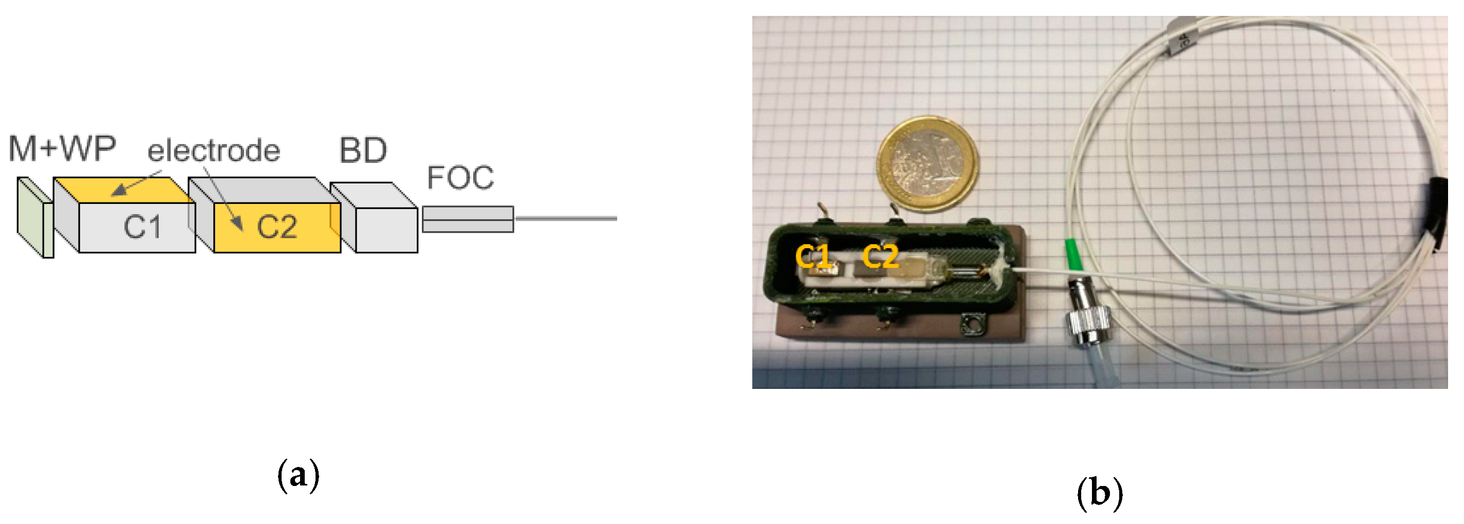
2. OVS Sensor Design Optimization

Figure 1a shows the retracing scheme of the OVS sensor [5]. In brief it is based on a standard optical single mode fibre collimator, for launching input light, with unknown polarization, toward the electric field transducer and to collect it back. The transducer consists of the following optical elements: a dielectric mirror, a λ/8 waveplate, a beam displacer (BD) and two Lithium Tantalate (LiTO3) crystals, rotated each other by 90°, in order to enhance the electric field sensitivity and at the same time to compensate for the natural birefringence of LiTaO3. All these optical components are designed to operate at a wavelength of 1550 nm. The voltage is applied perpendicularly to the direction of the input light through the metallization of the two lateral faces of the crystals.
In the OVS design it was taken into account the possible presence of critical gradients of the electric field inside the optical transducer, which could deteriorate the performances of the sensor over time. A COMSOL model of the transducer has been used for optimizing the settings of the geometric parameters (i.e., the distance between the various optical elements) in order to eliminate these effects. The assembly of the OVS sensor, shown in the picture of Figure 1b, consists of commercially available LiTaO3 crystals with 3 × 3 mm side dimensions placed at 2 mm distance. Using the finite element model, it was possible to preliminarily verify the correctness of the geometry adopted for the transducer and the absence of any alterations of the electric field in the interfacing region between the electrodes of two LiTaO3 crystals (Figure 2a); from the graph of Figure 2b, which shows the profile of the simulated electric field as a function of the distance between the two crystals, it turns out that, in the assessed optical layout, the gradient of the electric field is actually not critical.
A Medium Voltage capacitor divider with known and stable Voltage ratio, k, has been developed for housing the OVS sensor inside its body. At the voltage between 80% and 120% of the rated voltage (20 kVrms), as required for measuring purpose [6,7], the ratio error ε is lower than 0.2%: this confirms the good stability of the developed capacitive divider. Functional tests have been carried out on the OVS embedded assembly to verify the correct behavior and safety of the optical transducer either under simulated normal operating conditions and fast pulses as those foreseen in on service Medium Voltage Switchboards.

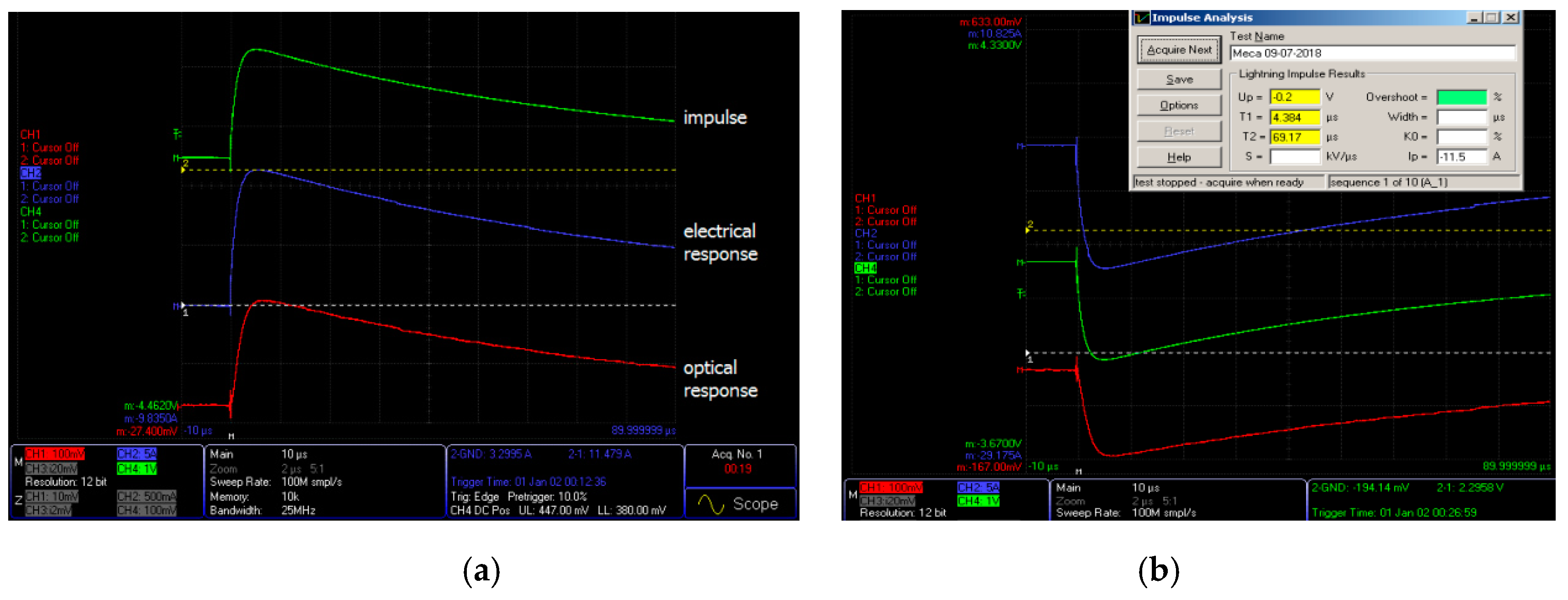
3. Results and Discussion

Figure 3 shows an example of the responses of the OVS sensor, embedded in the Medium Voltage Capacitive Divider, to the application of Voltage pulses.
Figure 3 shows the display of the oscilloscope with the optical response (red trace) to a 20 kVrms positive voltage pulse (green trace), 4 μs rise time and 55 μs duration. A rise time of 4.44 μs ± 0.05 μs was obtained from optical acquisitions for 10 negative and 10 positive consecutive pulses; this result demonstrate the effectiveness of the OVS sensor prototype to faithfully reproduce the voltage impulse features. No deterioration of the OVS sensor response was evidenced over time even in the presence of higher Voltage pulses (up to 50 kVrms), confirming the safety operation of the OVS sensor with the assessed optical assembly.

4. Conclusions

An optimization of the design of the Optical Voltage Sensor (OVS), developed for Medium Voltage measurements (amplitude, phase and frequency) as well as transient phenomena detection inside a MV capacitive divider, has been numerically performed to avoid possible inceptions of electrical field disturbances within the optical transduction path. The correct functionality of the assembled optical device has been verified under High voltage and impulse sources. During and after the tests, no malfunctions or damage of the OVS sensor were detected. It was also confirmed that, due to its intrinsic characteristics of a wide frequency band, the developed optical sensor is potentially capable of detecting fast voltage pulses.

Author Contributions

Conceptualization and methodology L.D.M., N.C.P. and A.O.; R.L.B. software; L.D.M., D.B. A.O. validation; L.D.M. writing—original draft preparation; N.C.P., R.L.B. and A.O. writing—review, supervision.

Funding

This work has been financed by the Research Fund for the Italian Electrical System under the Contract Agreement between RSE S.p.A. and the Ministry of Economic Development - General Directorate for Nuclear Energy, Renewable Energy and Energy Efficiency in compliance with the Decree of March 8, 2006.

Conflicts of Interest

The authors declare no conflict of interest.

References

  1. IEA Int. Energy Agency Report 2017 Digitalization & Energy. Available online: https://www.iea.org/publications (accessed on 5 November 2017).
  2. Bohnert, K.; Wildermuth, S.; Frank ABrändle, H. Fiber-optic voltage sensor using fiber gyro technology. In Proceedings of the Eurosensors XXIV Conference, Linz, Austria, 5–8 September 2010; pp. 1091–1094. [Google Scholar]
  3. Pan, F.; Xiao, X.; Xu, Y.; Ren, S. An Optical AC Voltage Sensor Based on the Transverse Pockels Effect. Sensors 2011, 11, 6593–6602. [Google Scholar] [CrossRef] [PubMed]
  4. Fusiek, G.; Nelson, J.; Niewczas, P.; Havunen, J.; Suomalainen, E.-P.; Hällström, J. Optical voltage sensor for MV networks. In Proceedings of the 2017 IEEE Sensors, Glasgow, UK, 29 October–1 November 2017; pp. 1–3. [Google Scholar]
  5. De Maria, L.; Pistoni, N.C.; Bartalesi, D. Combined optical sensor and capacitor voltage divider arrangement for Voltage control in Medium Voltage Switchboard. In Proceedings of the Eurosensors XXX, Budapest, Hungary, 4–7 September 2016; pp. 1597–1600. [Google Scholar]
  6. International Electrotechnical Commission. IEC 60044-7 Instrument Transformers—Part 7: Electronic Voltage Transformers. Additional Requirements for Electronic Voltage Transformers; IEC: Geneva, Switzerland, 1999. [Google Scholar]
  7. International Electrotechnical Commission. IEC 60060-2 High Voltage Test Techniques; IEC: Geneva, Switzerland, 2010. [Google Scholar]
Figure 1. OVS sensor. (a) retracing scheme of the optical transducer: fiber optic collimator (FOC), Lithium Tantalate (LiTO3) crystals (C1 and C2), Beam Displacer (BD), Mirror and λ/8 waveplate (M+WP); (b) picture of the developed OVS prototype [5].
Proceedings 15 00017 g001
Figure 2. COMSOL simulation of the electric field in the optical transducer generated (a) simulation of the electric field in the interfacing region between the two metal electrodes of the crystals at a 2 mm distance; (b) profile of the electric field as a function of the distance between the two LiTaO3 crystals.
Proceedings 15 00017 g002
Figure 3. Responses of the OVS sensor embedded in the Medium Voltage Capacitive Divider for applied (a) positive and (b) negative pulses (20 kVrms, rise time: 4 μs, green trace): comparison between the Capacitive Divider electrical (blue) and optical (red) outputs.
Proceedings 15 00017 g003

