Extended Abstract

Control of a Boost Converter to Improve the Performance of a Photovoltaic System in a Microgrid †

by
Miguel Ángel Abundis Fong
1,
Jaime José Rodriguez Rivas
1,
Oscar Carranza Castillo
1,2,*,
Rubén Ortega Gonzalez
1,2 and
Juan Carlos Tellez Barrera
2
1
Instituto Politécnico Nacional, Escuela Superior de Ingeniería Mecánica y Eléctrica, Ciudad de México 07738, Mexico
2
Instituto Politécnico Nacional, Escuela Superior de Computo, Ciudad de México 07320, Mexico
*
Author to whom correspondence should be addressed.
Presented at Environment, Green Technology and Engineering International Conference (EGTEIC 2018), Caceres, Spain, 18–20 June 2018.
Proceedings 2018, 2(20), 1270; https://doi.org/10.3390/proceedings2201270
Published: 30 October 2018

Abstract

:
In this work, the analysis of a CD-CD converter type Boost is presented. This converter works in Discontinuous Conduction Mode; In addition, the design of its control loops is performed, using an Average Current Mode control. The Boost converter is part of a photovoltaic generation system using solar panels. The photovoltaic system is established in a microgrid, with which the inverter works in grid mode and island mode. The main objective of the Boost convertor is to raise and regulate the voting from the solar panels to feed a single-bridge full-bridge inverter. The controllers designed for the boost converter are validated by simulation. The results obtained prove that the designed controller has an acceptable transient response to disturbances in the system input and adequately analyzing overdrafts and establishment times when disturbances are generated.

1. Introduction

In current power electrical systems, greater participation of renewable energy sources is obtained. Photovoltaic solar energy is one of the most developed renewable sources in recent years. These generation systems have the disadvantages of low efficiency and low power, in addition to being intermittent throughout the day. It is necessary to have electronic converters that accurately regulate the levels of energy generated and distribute it to their loads, complying with the amplitude and frequency established, and with the total harmonic distortion levels allowed.
A robust ACC model is described in [1] to decrease the limitations derived from zero in the right half-plane of the output voltage transfer function to the control. However, both works contemplate only the operation in island mode. The transition between the island and grid devices is studied in [2] for the operation in CCM, thus presenting the effect of reverse recovery in the Boost.
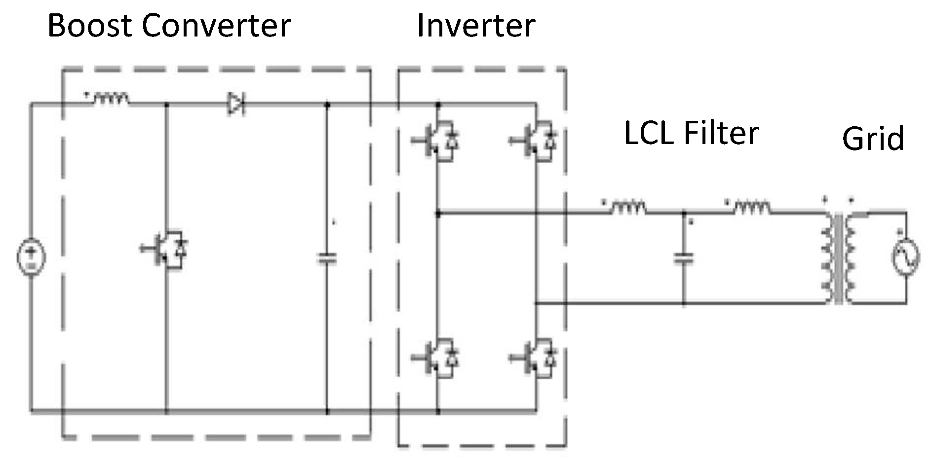
In the present paper, ACC control is proposed as a control scheme of a Boost converter, which is part of a photovoltaic generation system. The Boost converter operates in the Discontinuous Conduction Mode (DCM) a way to avoid the effect of reverse recovery on the power switch [3]. The system is contemplated to operate in Island mode, feeding a load; as well as, for its operation in grid mode, injecting the energy into the grid. Figure 1 shows the system circuit for island mode, and Figure 2 for grid mode. The inverter and the filter are beyond the scope of this paper.

2. Boost Converter

To perform the analysis of the behavior of the Boost converter, since this is a non-linear circuit, a linear equivalent circuit must be obtained around an operating point. For this, the PWM switch method [4] is used. For the equivalent circuit in island mode, the load fed by the converter is modeled by a resistor; and in the case of the equivalent grid mode circuit, the Boost output has a CD source as a load, because in this operating mode, it is the inverter that controls the voltage on the CD Bus. For the photovoltaic system it is considered an array of solar panels that delivers a maximum power of 2 kW in both modes, with a voltage of 96 V. For the Boost converter the nominal values shown in Table 1 are considered. The switching frequency of The IGBT power switches is 10 kHz.
In island mode, the Boost converter is responsible for regulating the DC bus voltage, for this purpose the ACC scheme is used, as shown by Figure 3, where RiBI is the gain of the current sensor, βB is the gain of the voltage sensor, FmB is the gain of the PWM modulator that is related to the peak value of the sawtooth comparator signal and DG (s) represents a digital delay necessary for the implementation of the controllers by means of a Digital Processor. Signals (DSP). In grid mode, the voltage on the CD Bus is regulated by the inverter. Therefore, the Boost is controlled only through the current loop, which is responsible for maintaining the required average current value of the inductor. The block diagram of the control loop is shown by Figure 4.
F m B = 1 V p p = 1 1 = 1 ,   R i B = 0.042   and   β i B = 0.015
The digital delay transfer function DG (s) is given by the Padé approximation and it is shown by (2), where Tmu is the sampling period.
D G ( s ) 1 ( s T m u 2 ) + ( ( s T m u ) 2 12 ) 1 + ( s T m u 2 ) + ( ( s T m u ) 2 12 )
The variable to be controlled in the internal loop is the average current flowing through the inductor, which corresponds to the average input current to the converter. The transfer function that is used for this control loop is GidB (s) that relates the current in the inductor iL with respect to the variation of the duty cycle d of the circuit breaker, which is shown in (4), and where YL is the admittance of the inductor with its internal resistance in series and Yo is the admittance of output.
Y L ( s ) = 1 Z L ( s ) = 1 R L + s L
Y O ( s ) = 1 Z O ( s ) = s C ( R C + R L O A D ) + 1 R L O A D ( s C R C + 1 )
It is obtained the transfer function that relates the current in the inductor to the duty cycle of the switch in grid mode.
G idB ( s )= i L ^ d ^ | V ^ in =0 = Y L [ ( Y o + g o )( k i + k o )( k o g o ) ] ( Y o + g o )( Y L + g i + g o + g f ) g o ( g o + g f )
The open loop transfer function and closed-loop transfer function are expressed by:
T i ( s ) = F m R i G i B I ( s ) G i d B ( s ) D G ( s )   and   G i c B ( s ) = i L ^ v c ^ = ( 1 + G i B I ( s ) ) ( F m D G ( s ) G i d B ( s ) ) ( 1 + T i )
The controllers of all the loops are tuned following the stability criterion of Bode. Minimum values are a Phase Margin (MF) of 50° and a Gain Margin (MG) of 7 dB [4]. Therefore, the tuned current controller is expressed by (7). The tuned compensator has a magnitude of −51.2 dB at the switching frequency.
G i B I ( s ) = 0.0026342 ( s + 19637 ) ( s )
For the external voltage loop, the transfer of interest function is that which relates the output voltage of the converter with the output signal of the voltage compensator, shown in (19).
G cB ( s )= v ^ 0 v c ^ = [ ( g f + g o )( k i + k o )( k o )( Y L + g i + g o + g f ) ] F m [ ( 1+ G idB )( R iB G BI DG G icB ) ] ( Y o + g o )( Y L + g i + g o + g f ) g o ( g o + g f )
For the open loop transfer function, the digital delay is not taken into account, since it is included in the internal loop of current and its effect on the external loop is negligible. Therefore, the open loop function and the closed loop function are expressed by:
T v ( s ) = G v c B ( s ) β i B G v B I ( s )   and   G v r B ( s ) = G v B ( s ) G v c B ( s ) ( 1 + T v ( s ) )
The tuned compensator is shown by (10). The loop bandwidth is 14 Hz, the Gain Margin is 97.6 dB, and the Phase Margin is 84.3°. To avoid changes of compensators when working in grid mode and in island mode, the same current compensator used in island mode (7) is used.
G v B I ( s ) = 0.0057981 ( s + 72856 ) ( s )
The open-loop transfer function and closed-loop transfer function are expressed by:
T i G ( s ) = G i D B G ( s ) R i B D G ( s ) F m G i B G ( s )   and   G i c B G ( s ) = G i d B G ( s ) D G ( s ) F m ( 1 + G i B G ( s ) ) ( 1 + T i G ( s ) )
The bandwidth of the loop is 92 Hz, the Gain Margin is 46.2 dB, and the Phase Margin is 69°.

3. Results

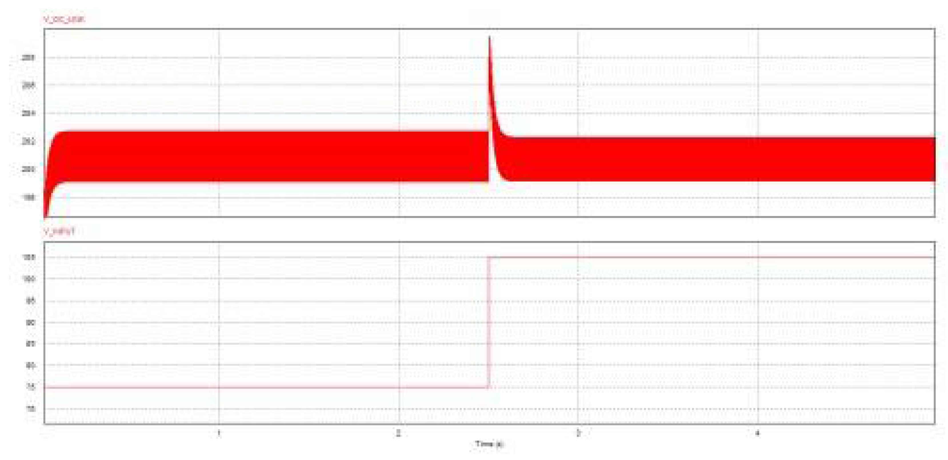
The results are presented in simulation of the system under study and the proposed control loops. The system is simulated including disturbances in the input voltage, which represents the variation in the output of the photovoltaic panel. Figure 5 shows that the Boost provides the desired average voltage value even when there is a disturbance in the input voltage; there is a maximum overdraft of 4.7% of the reference value, with a settling time of 0.2 s.
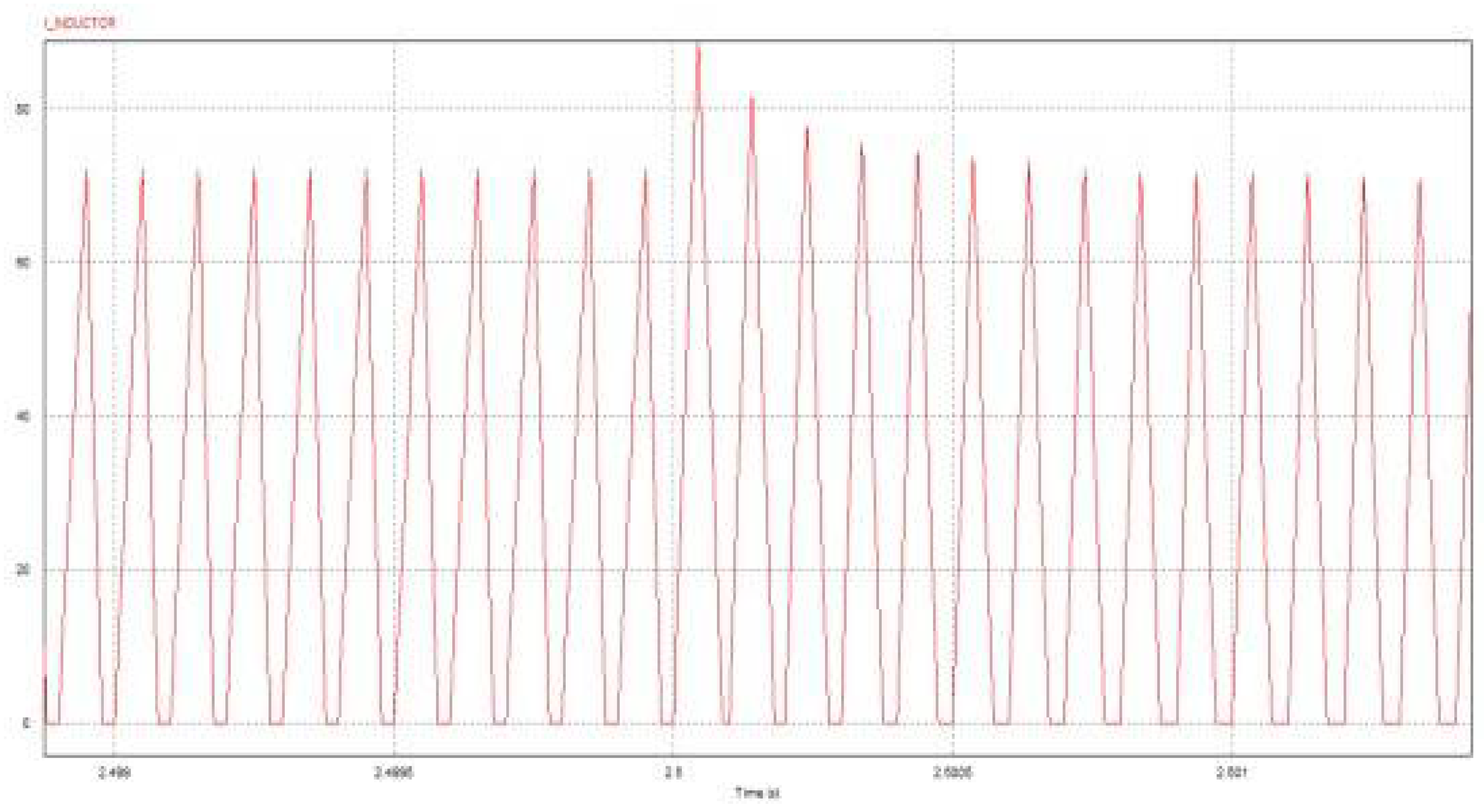
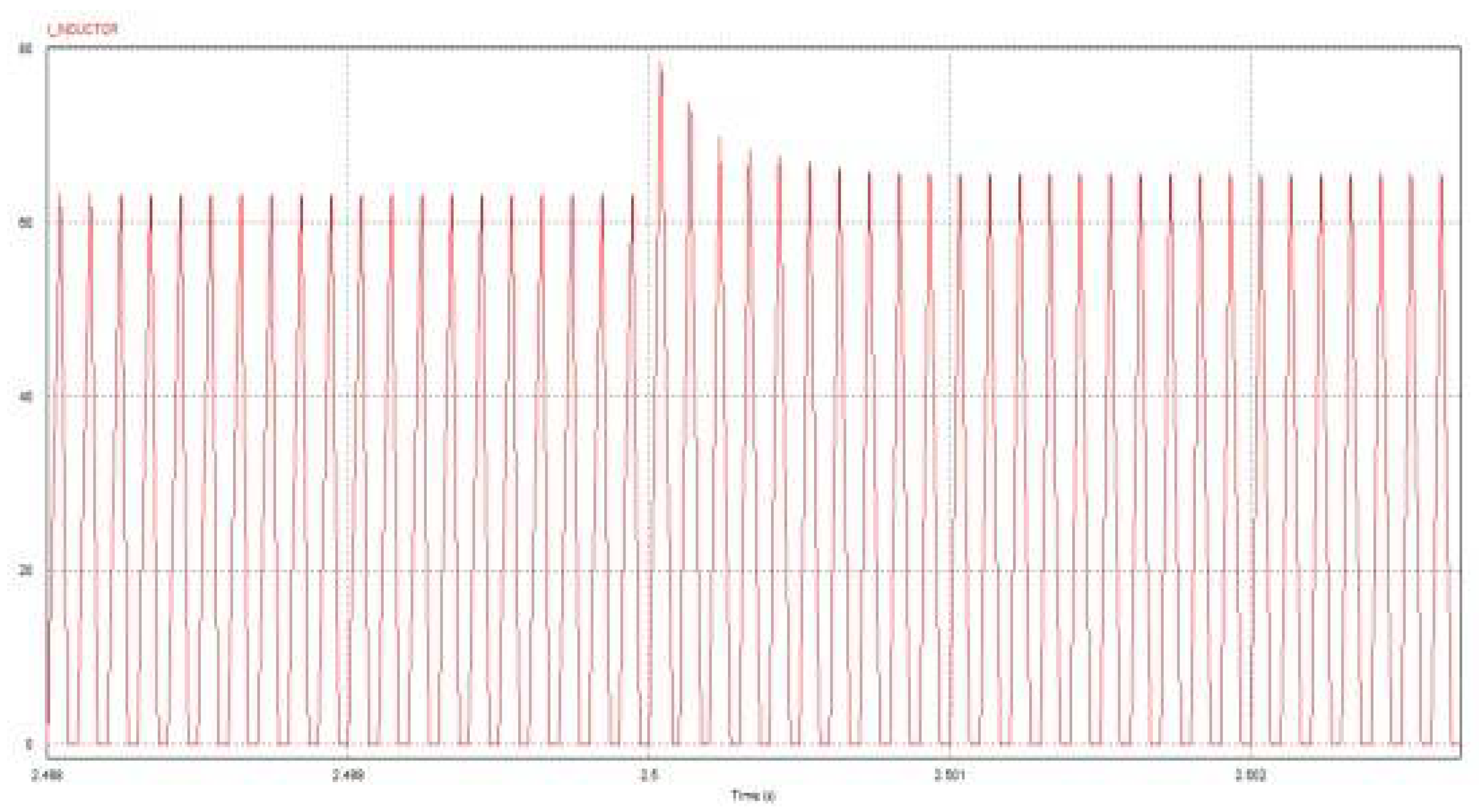
The disturbances considered are in the range of 75 V to 105 V. Figure 6 shows that the current in the inductor remains in DCM and that its average value is the required 22 A. In Figure 7, the current in the inductor that remains in DCM and with an average value of 22 A for the grid mode is shown, close to the moment of the disturbance, which is at 2.5 seconds for both modes of operation.

4. Conclusions

In this paper we present an average current mode control scheme for a Boost converter operating in Island mode and in Network mode. The designed controllers of the voltage and current loops are of the PI type. The controllers are validated through the simulation of the system in PSIM, where it is observed that the requirements for maximum overdraft and settling time are met, during the transitory response to disturbances in the system input.

References

  1. Benavent, J.M.; Figueres, E.; Garcera, G.; Pascual, M. Robust Model-Following Regulator for Average Current-Mode Control of Boost DCDC Converters. In Proceedings of the 2005 IEEE International Symposium on Industrial Electronics, Dubrovnik, Croatia, 20–23 June 2005. [Google Scholar]
  2. Carrillo, F. Transition controllers between Island and Grid mode of a Photovoltaic system in a Smart Grid. In Proceedings of the VIII Congreso Internacional de Ingeniería Electromecánica y de Sistemas, CDMX, Ciudad de México, Mexico, 17-21 October 2016. [Google Scholar]
  3. Mohan, N. Power Electronics, Converters, Applications and Design, 3rd ed.; Wiley: Hoboken, NJ, USA, 2003. [Google Scholar]
  4. Garcerá, G.; Figueres, E.; Abellán, A. Conversores Conmutados: Circuitos de Potencia y Control; Universidad Politécnica de Valencia: València, Spain, 1998. [Google Scholar]
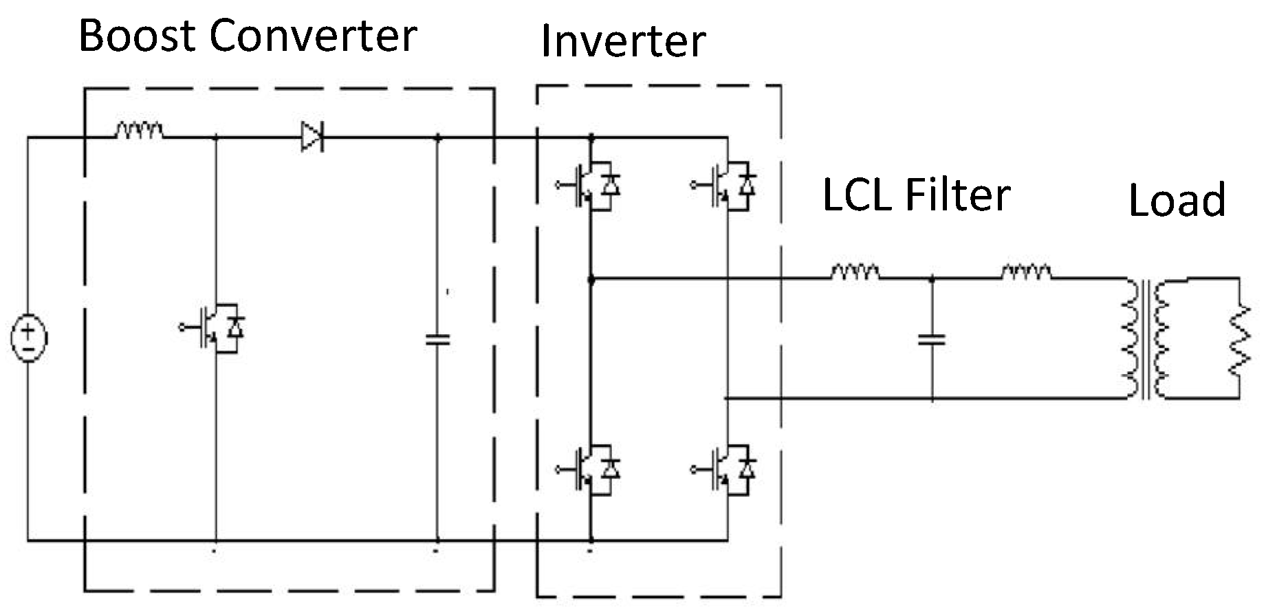
Figure 1. Photovoltaic system in island mode.
Proceedings 02 01270 g001
Figure 2. Photovoltaic system in grid mode.
Proceedings 02 01270 g002
Figure 3. Block diagram in Island mode.
Proceedings 02 01270 g003
Figure 4. Block diagram in grid mode.
Proceedings 02 01270 g004
Figure 5. Voltage on the DC Bus and input voltage to the converter in Island mode.
Proceedings 02 01270 g005
Figure 6. Transient response of the current in the inductor in the Island mode.
Proceedings 02 01270 g006
Figure 7. Transient response of the current in the inductor in the grid mode.
Proceedings 02 01270 g007
Table 1. Boost converter nominal values.
Element Value
Output power, Pout 2000 W
Output voltage, Vout 200 V
Output current, Iout 10 A
Load resistance, RLOAD 20 Ω
Inductor resistance, RL 75 mΩ
Inductor, L 50 μH
Capacitor resistance, RC 50 mΩ
Capacitor, C 1.1 mF
Publisher’s Note: MDPI stays neutral with regard to jurisdictional claims in published maps and institutional affiliations.