Proceeding Paper

Electromagnetic Characterization of Engineered Materials Using Capacitively Loaded Aperture Sensors †

by
Oleksandr Malyuskin
Queen’s University Belfast, ECIT, Centre for Wireless Innovation, Belfast BT3 9DT, UK
Presented at the 6th International Electronic Conference on Sensors and Applications, 15–30 November 2019; Available online: https://ecsa-6.sciforum.net/.
Proceedings 2020, 42(1), 31; https://doi.org/10.3390/ecsa-6-06576
Published: 14 November 2019

Abstract

:
A novel method for electromagnetic (EM) characterization of engineered artificial materials such as biomaterials, nanomaterials, and composite materials is proposed and experimentally evaluated in this paper. The method is based on resonance transmission properties of capacitively loaded apertures in conductive screens. The advantage of this new method over the existing techniques (free space, loaded waveguide, microstrip and coplanar waveguide resonators, coaxial probe, etc.) is three-fold: (i) resonance EM field enhancement inside the loaded aperture leads to very high sensitivity and therefore accuracy of EM parameters de-embedding, (ii) only small thin samples of material under test are required (with a sample area substantially smaller than squared wavelength of radiation, ~0.01 λ2), (iii) the method is easily scalable over the frequency and wavelength and based on relatively simple permittivity and permeability de-embedding procedure. The experimental setup in the microwave S-band (2–3 GHz) is based on two dipole antennas, capacitive aperture in the conductive screen, unloaded and loaded with material under test, and vector network analyzer (VNA) for signal generation and data acquisition. Analytical de-embedding procedure is developed and applied to the characterization of carbon nanotube (CNT) material microwave absorption. It is demonstrated that the method offers very high accuracy in material characterization based on minimal material samples.

1. Introduction

Electromagnetic (EM) characterization of engineered artificial materials such as composites, nano- and biomaterials is very important for several reasons. One of these reasons is future proliferation of 5G communication networks [1] exposing urban population into the EM radiation of wide spectral range. Therefore, it is critically important to understand how the new materials EM response can be utilized in electronic and communication devices and also to ensure the EM compatibility of biomaterials used in human body. The future smart fabrication, construction engineering, aerospace, and automotive industries would also benefit from online in-situ characterization of composite materials [2] used in structures and constructions.
Microwave material characterization methods [3,4,5,6] are well established and can be classified into several categories based on the microwave measurement setup: coaxial probe, transmission line, waveguide, free-space, resonant cavity or resonator, and parallel plate techniques [5,6,7,8,9]. As a rule, application of these methods requires a relatively large material sample (~0.125λ2 in waveguide-based measurement methods or >λ2 for free space setup, λ is a wavelength of radiation) or material that can be filled inside a specific shape (e.g., resonator cavity).
In this paper, we propose a new method that can be considered as a combination of free-space, parallel-plate, and resonator-based methods [5]. This method allows us to characterize dielectric permittivity and/or electromagnetic absorption (conductivity) and only requires a very small quantity of material (~0.0125 λ2 or smaller cross-sectional area). The material sample could be in the form of very thin sheet (thickness ~1 µm–10 µm). This method can be easily scaled in the frequency/wavelength range, it features straightforward permittivity de-embedding algorithm and requires simple microwave or mm-wave measurement setup consisting of a pair of dipole antennas and capacitively loaded aperture in a conductive screen. Since the method is based on resonant microwave transmission, the signal generation and acquisition circuit topology is simple since it does not require the measurement of the reflected signal for reference. The signal chain circuit requires inexpensive electronic hardware, which makes this method very attractive for in-situ automated applications.

2. Materials and Methods

2.1. Measurement Setup Geometry

The geometry of the measurement setup is shown in Figure 1. The setup consists of two dipole antennas, transmit (TX) and receive (RX), located in the near (doffset ≈ 0.1λ–0.25λ), Fresnel (doffset ≈ 0.25λ–0.5λ) or far field (doffset > λ) zones with respect to the aperture in the conductive screen. Due to the differential nature of the measurement, the system will operate irrespectively of the antennas distance from the aperture.

2.2. EM Field Enhancement in the Capacitevely Loaded Aperture

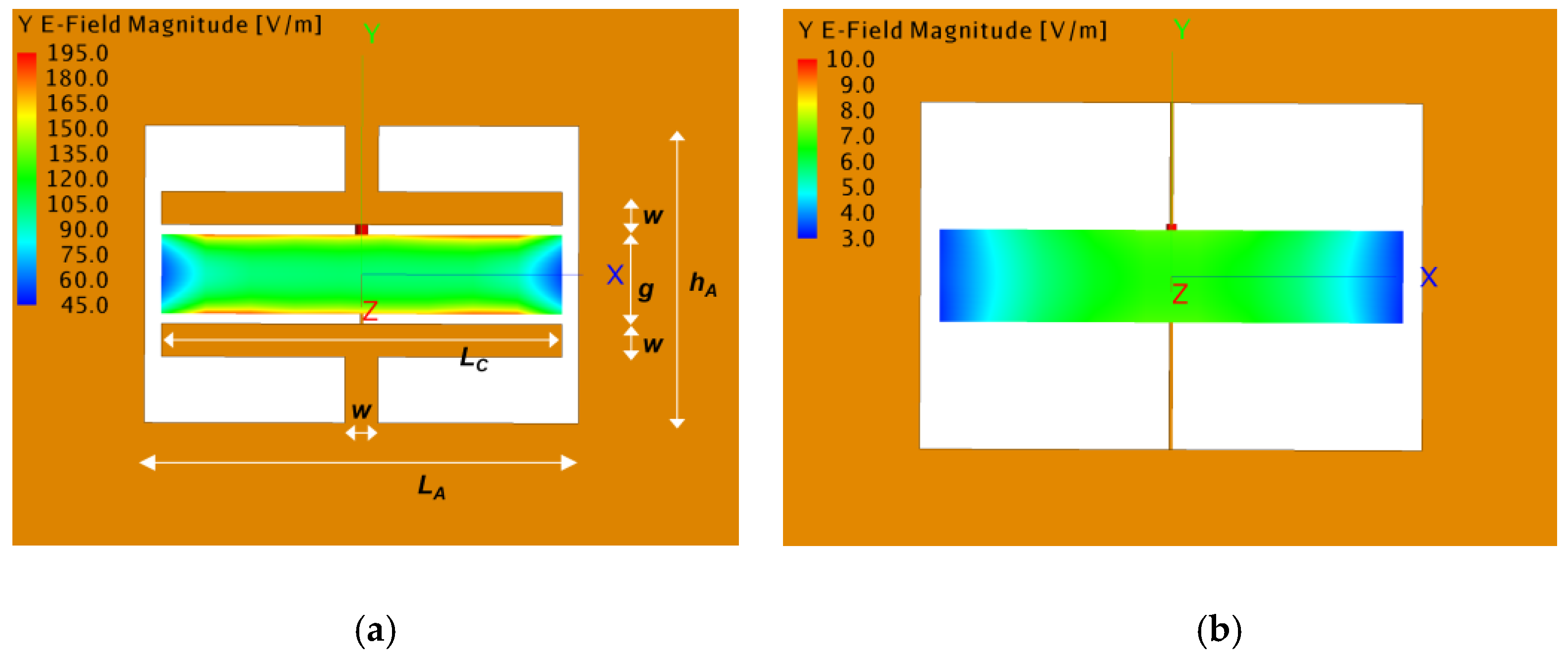
Figure 2a shows simulated E-field enhancement inside capacitively loaded aperture designed to operate at 2.42 GHz. These results are obtained with commercial full-wave FEKO solver. The dimensions of the capacitively loaded aperture are LA = 26 mm, LC = 24 mm, hA = 18 mm, g = 6 mm, and w = 2 mm. The unloaded rectangular aperture in Figure 2b has dimensions of 26 mm × 18 mm.
It can be seen that at the resonance, E-field is significantly enhanced (20 times) in the capacitive aperture compared to the unloaded rectangular aperture. This leads to strong EM interaction between the field in the capacitively loaded aperture and the material sample under test.
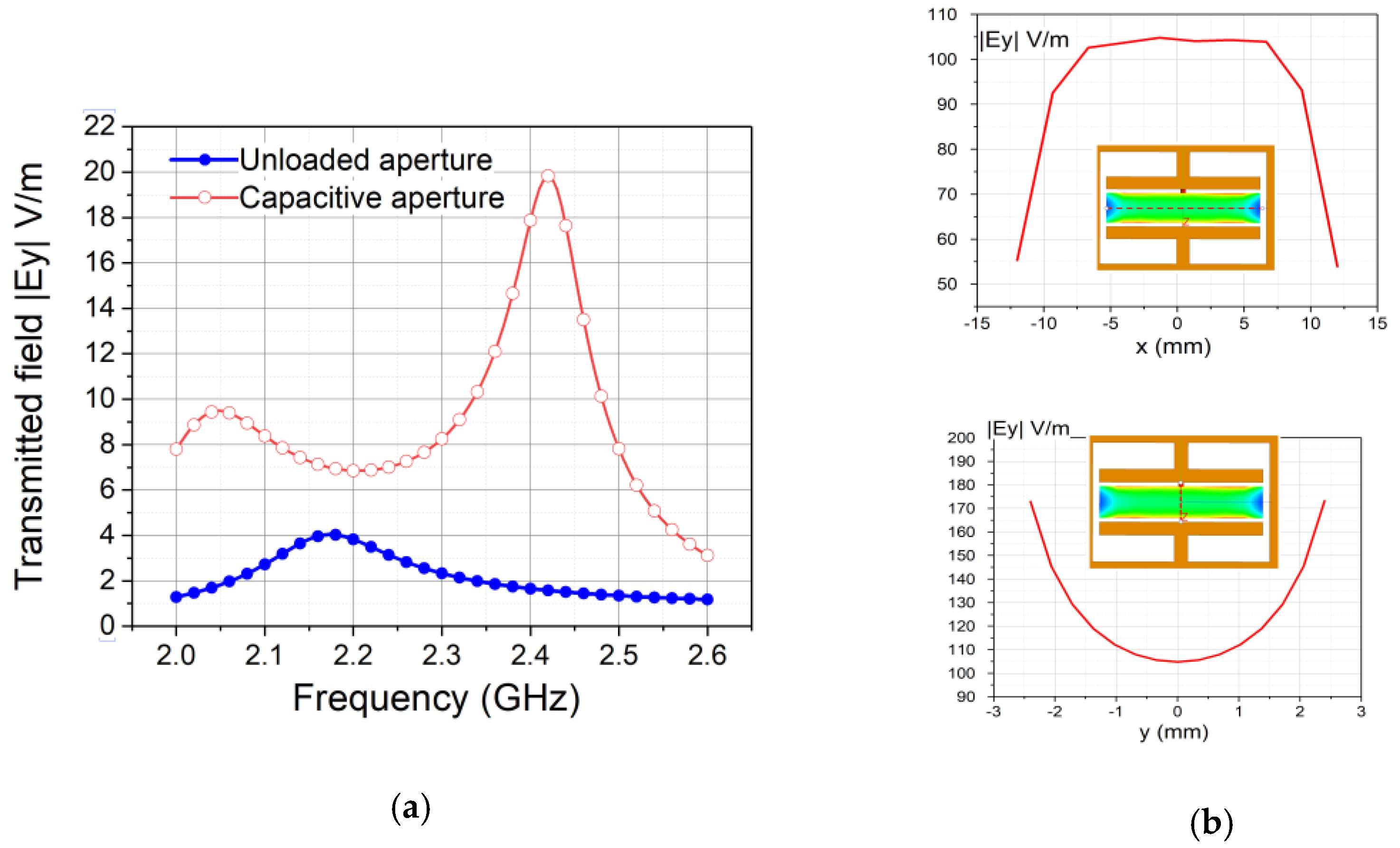
Figure 3a shows the resonance characteristics of the transmitted field at 10mm stand-off distance from the aperture on z axis (0, 0, 10 mm). It can be seen that a capacitively loaded aperture leads to very strong resonance transmission as compared to the unloaded aperture case. Figure 3b shows dominant Ey-field component inside the aperture “capacitor”. It is interesting to note that while the Ey-field is uniform along x, it changes parabolically along the vertical y direction.

2.3. Material Sample Permitivity and EM Loss Characterization Using Equivalent Circuit Model

In order to develop EM parameters de-embedding procedure, let us consider the equivalent circuit model of the capacitively loaded aperture with and without the material sample, Figure 4.
In Figure 4 the equivalent lump parameters are derived from the EM [10,11]. Unloaded aperture capacitance C0 and inductance L0 are given by the following expressions:
1 C 0 = 1 4 π ε 0 | q 0 | 2 S g ρ ( r ) ρ ( r ) |rr| drdr
L 0 = Sg H · r d r d r / < I 0 >
where q0 and <I0> are maximum time-average charge across the aperture, “capacitor” plates and average maximum current delivered to the aperture “capacitor”. ZFS is a characteristic impedance,
Z F S = E y / H x
In general, ZFS is a complex number if the TX/RX antennas are located in the near or Fresnel field zone. In (1) and (2), the integration is carried out over the Sg “capacitive gap” area shown in Figure 2a.
Consider the situation, when the capacitive aperture is loaded with thin dielectric material which does not appreciably change the aperture self-inductance. Next, assuming that the E-field is approximately uniform inside the capacitive gap (more accurate study taking into account spatial field variation, Figure 3b will be reported in full paper), it is possible to derive the ratio of the resonance frequencies of empty, f r e s ( 0 ) ,   and sample-loaded, f r e s ( L ) ,   capacitive apertures as follows:
f r e s ( 0 ) / f r e s ( L ) = A κ + 1
where κ = R e   ε is the real part of the relative complex-valued material permittivity ε and A is a constant that depends on the aperture geometry and can be calculated using quasi-static capacitance of parallel strips [12,13]
A = w ln ( 1 + g / w ) / π g
From (4), (5) the real part κ   of the relative permittivity of material can be found as follows:
κ = A 1 ( ( f r e s ( 0 ) / f r e s ( L ) ) 2 1 )
To characterize EM loss due to material, it is possible to employ energy conservation law to find the imaginary part κ = I m   ε     of the relative permittivity of the material. It is possible to write the power balance for the unloaded and loaded apertures as
P i n ( f r e s ( 0 ) ) = P r a d ( f r e s ( 0 ) ) + P s t ( f r e s ( 0 ) ) , P i n ( f r e s ( L ) ) = P r a d ( f r e s ( L ) ) + P s t ( f r e s ( L ) ) + P l o s s ( f r e s ( L ) )
where P i n , P r a d , P s t and P l o s s are incident, radiated, stored and loss power of the capacitive aperture respectively [14]. Recalling that the loss power [14] is given by the expression
P l o s s = κ / κ
and the stored power for the unloaded and loaded apertures can be written in the form
P st ( f res ( 0 ) ) = Q 0 P rad ( f res ( 0 ) ) , P st ( f res ( L ) ) = Q L ( P rad ( f res ( L ) ) + P loss ( f res ( L ) ) )
It is possible, by normalizing (7) by the incident power, and combining (7)–(9) to obtain the expression for the imaginary relative permittivity κ in terms of the real part κ , normalized (by incident power) transmission parameters S ¯ 21 and Q-factors of the loaded and unloaded apertures,
κ = κ [ | S ¯ 21 2 ( f r e s ( 0 ) ) | 1 + Q 0 1 + Q L | S ¯ 21 2 ( f r e s ( L ) ) | ]

3. Experimental Results and Discussion

Initial experimental results are presented in Figure 5 for the case of carbon nanotube (CNT) material. There are several interesting observations can be made from the experimental data.
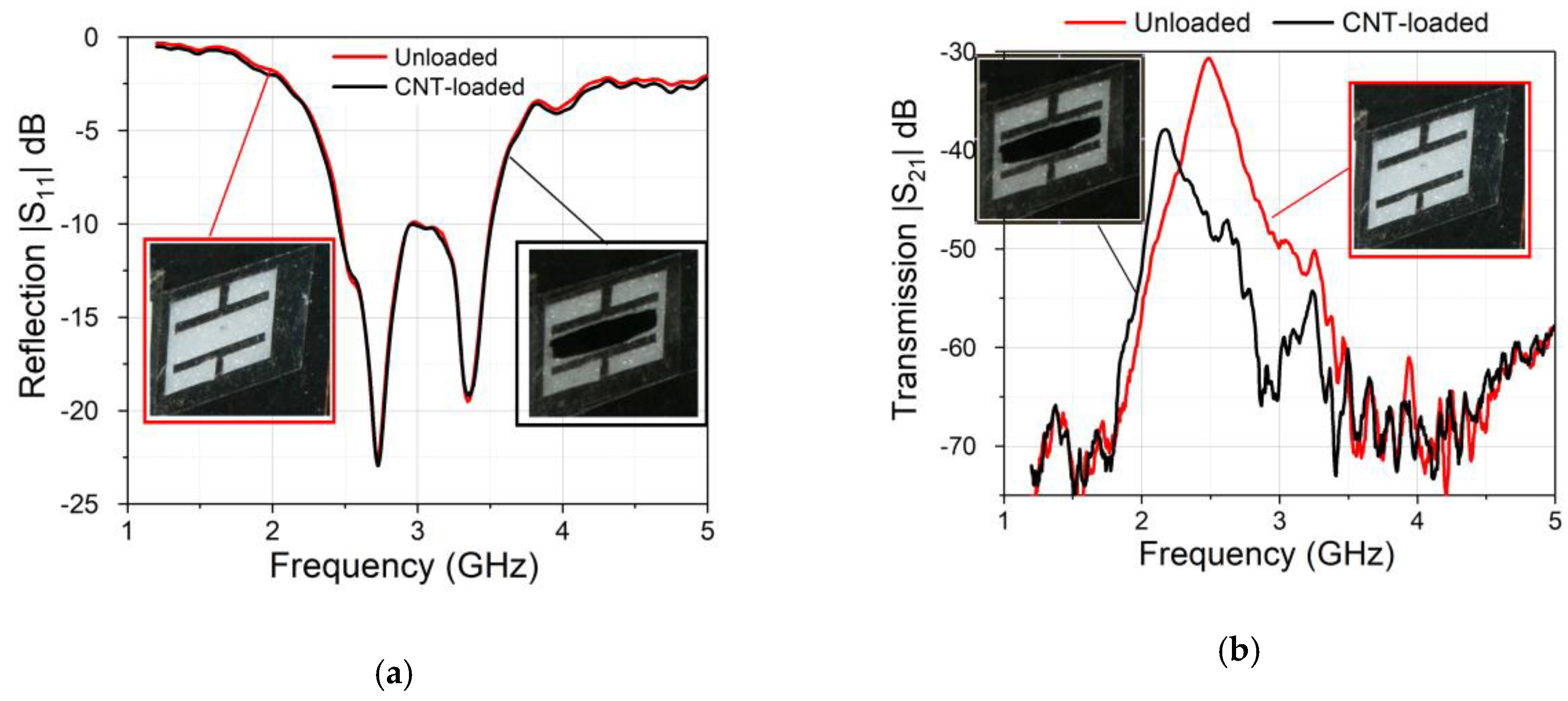
First, it can be clearly seen in Figure 5a that the aperture operates in reflection-less regime, when all the radiation from a TX antenna is transmitted through. This simplifies the analysis and de-embedding of material parameters. It is possible to apply approximate formulas (6)–(10) to extract material parameters of the CNT material from the transmission data as shown in Figure 5b. The results are summarized in the Table 1.
The data in Table 1 show that the CNT material introduces high loss at 2–3 GHz range, tan δ = 1.03 with very moderate value of the real part of wavenumber κ .
The permittivity de-embedding procedure proposed here is based on the approximation of capacitively loaded aperture as a high-frequency capacitor with subsequent use of low-frequency formulas for the resonance frequency shift and quality factors of a loaded capacitor. A more accurate de-embedding procedure based on full wave EM field calculations will be reported elsewhere in future.

Acknowledgments

The author is thankful to Davide Mariotti and Paul Brunet for providing CNT material samples and helpful discussions.

Conflicts of Interest

The author declares no conflict of interest.

References

  1. Yang, P.; Xiao, M.; Li, S. 6G Wireless Communications: Vision and Potential Techniques. IEEE Netw. 2019, 33, 70–75. [Google Scholar] [CrossRef]
  2. Kharkovsky, S.; Zoughi, R. Microwave and millimeter wave nondestructive testing and evaluation—Overview and recent advances. IEEE Instrum. Meas. Mag. 2007, 10, 26–38. [Google Scholar] [CrossRef]
  3. Kaatze, U. Techniques for measuring the microwave dielectric properties of materials. Metrologia 2010, 47, S91–S113. [Google Scholar] [CrossRef]
  4. Brodie, G.; Jackob, M.; Ferrell, P. 6 Techniques for Measuring Dielectric Properties. In Microwave and Radio-Frequency Technologies in Agriculture; Sciendo: Berlin, Germany, 2015. [Google Scholar]
  5. Basics of Measuring the Dielectric Properties of Materials, Keysight. Available online: http://literature.cdn.keysight.com/litweb/pdf/5989-2589EN.pdf (accessed on 21 October 2019).
  6. Baker-Jarvis, J.; Janezic, M.; Degroot, D. High-Frequency Dielectric Measurements. Part 24 in a Series of Tutorials on Instrumentation and Measurement. IEEE Instrum. Meas. Mag. 2010, 13, 24–31. [Google Scholar] [CrossRef]
  7. Akhtar, M.J.; Feher, L.E.; Thumm, M. A closed-form solution for reconstruction of permittivity of dielectric slabs placed at the center of a rectangular waveguide. IEEE Geosci. Remote Sens. Lett. 2007, 4, 122–126. [Google Scholar] [CrossRef]
  8. Mirzavand, R. Honari, M.M.; Mousavi, P. High-Resolution Dielectric Sensor Based on Injection-Locked Oscillators. IEEE Sens. J. 2018, 18, 141–148. [Google Scholar] [CrossRef]
  9. Vlachogiannakis, G.; Hu, Z.; Shivamurthy, H.T.; Neto, A.; Pertijs, M.A.; de Vreede, L.C.; Spirito, M. Miniaturized Broadband Microwave Permittivity Sensing for Biomedical Applications. IEEE J. Electromagntics RF Microw. Med. Biol. 2019, 3, 48. [Google Scholar] [CrossRef]
  10. Butler, C.; Rahmat-Samii, Y.; Mittra, R. Electromagnetic penetration through apertures in conductive surfaces. IEEE Trans. Antennas Propagat. 1978, EMC-20, 82–93. [Google Scholar] [CrossRef]
  11. Balanis, C. Antenna Theory: Analysis and Design; John Wiley & Sons: Hoboken, NJ, USA, 2016. [Google Scholar]
  12. Malyuskin, O.; Fusco, V. High-Resolution Microwave Near-Field Surface Imaging Using Resonance Probes. IEEE Trans. Instrum. Meas. 2016, 36, 189–200. [Google Scholar] [CrossRef]
  13. Zypman, F. Mathematical expression for the capacitance of coplanar strips. Journ. Electrostatics 2019, 101, 103371. [Google Scholar] [CrossRef]
  14. Kajfez, D.; Guillon, P. (Eds.) Dielectric Resonators; Artech House: London, UK, 1986. [Google Scholar]
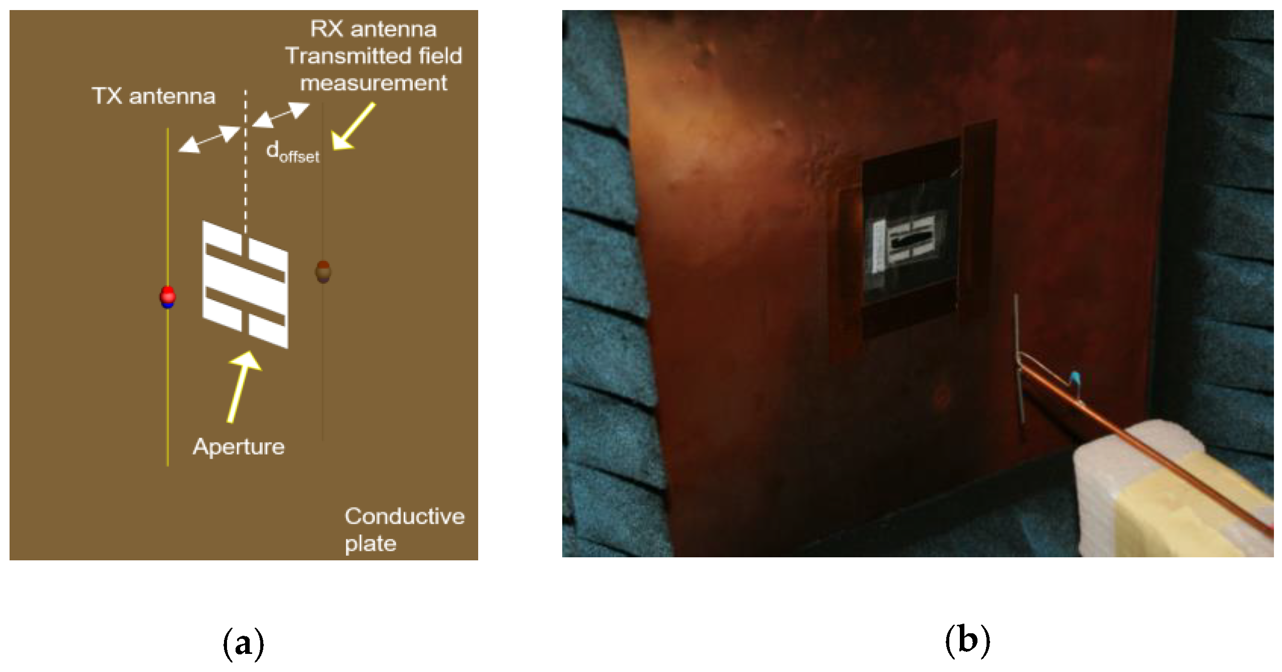
Figure 1. (a) Geometry of measurement setup. (b) Capacitive aperture loaded with carbon nanotube material in the anechoic measurement environment.
Proceedings 42 00031 g001
Figure 2. E-field inside the capacitively loaded and unloaded apertures at transmission resonance. (a) Ey-field magnitude inside the capacitively loaded aperture at 2.42 GHz. (b) Ey-field magnitude in unloaded rectangular aperture at 2.176 GHz.
Proceedings 42 00031 g002
Figure 3. (a) Transmitted Ey-field magnitude 10mm off the aperture on z axis (0, 0, 10 mm). The aperture is excited by a half-wavelength y-oriented dipole antenna with the centre located at (0, 0, −10 mm). (b) Ey-field magnitude distribution inside capacitive aperture at 2.42 GHz, red dashed lines show the field sampling points.
Proceedings 42 00031 g003
Figure 4. Equivalent electric lumped-element circuits of capacitive aperture, unloaded and loaded with material sample.
Proceedings 42 00031 g004
Figure 5. (a) Reflection parameter magnitude |S11|of the loaded and unloaded apertures in the S-band. (b) Transmission parameter |S21|, the aperture has dimensions LA = 26 mm, LC = 24 mm, hA = 18 mm, g = 6 mm, w = 2 mm.
Proceedings 42 00031 g005
Table 1. Experimental values of resonance frequencies, Q-factors of the aperture and reconstructed relative permittivity of material under test.
f r e s ( 0 ) Q 0 f r e s ( L ) Q L κ κ
2.485 GHz 14.22.170 GHz11.42.122.18
Publisher’s Note: MDPI stays neutral with regard to jurisdictional claims in published maps and institutional affiliations.