Abstract

Pull-In Voltage and Stress in Fixed-Fixed Beams of RF MEMS Switches †

1
IMM-CNR, Institute for Microelectronics and Microsystems, National Research Council, Via Monteroni, 73100 Lecce, Italy
2
SD FBK, Center for Sensors and Devices, Fondazione Bruno Kessler, Via Sommarive 18, Povo, 38123 Trento, Italy
*
Author to whom correspondence should be addressed.
Presented at the XXXV EUROSENSORS Conference, Lecce, Italy, 10–13 September 2023.
Proceedings 2024, 97(1), 174; https://doi.org/10.3390/proceedings2024097174
Published: 10 April 2024

Abstract

:
Electrostatically actuated microelectromechanical system (MEMS) switches with fixed- fixed beams were fabricated. FEM modeling was used to calculate the contributions of stress in the fabricated beams from the measured values of pull-in voltage. The reported study provides useful guidelines to optimize the design of fixed-fixed beams, in order to reduce the stress contributions for the successful development of efficient and reliable electrostatically actuated MEMS devices.

1. Introduction

Different geometries of beams and/or actuation pads have been proposed [1] to reduce the pull-in voltage of RF MEMS switches, also taking into account the residual stress of the suspended beam. However, to our knowledge, only in few works [2] have the theoretical values of the residual stress been combined with experimental values of the pull-in voltage and/or spring constant for a variety of beams with different geometric parameters.
Here, electrostatically actuated RF MEMS switches with fixed-fixed beams were fabricated, using a surface micromachining approach. FEM modelling was used to evaluate the residual stress, which is consistent with the measured increase of the pull-in voltage. Moreover, the distribution of the stress, which is induced by the electrostatic actuation force, is calculated.

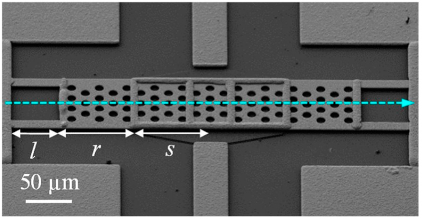
2. Materials and Methods

An eight-mask process was used to fabricate capacitive RF MEMS switches with fixed-fixed beams (Figure 1). Details on the beam fabrication process are reported in Ref. [3].

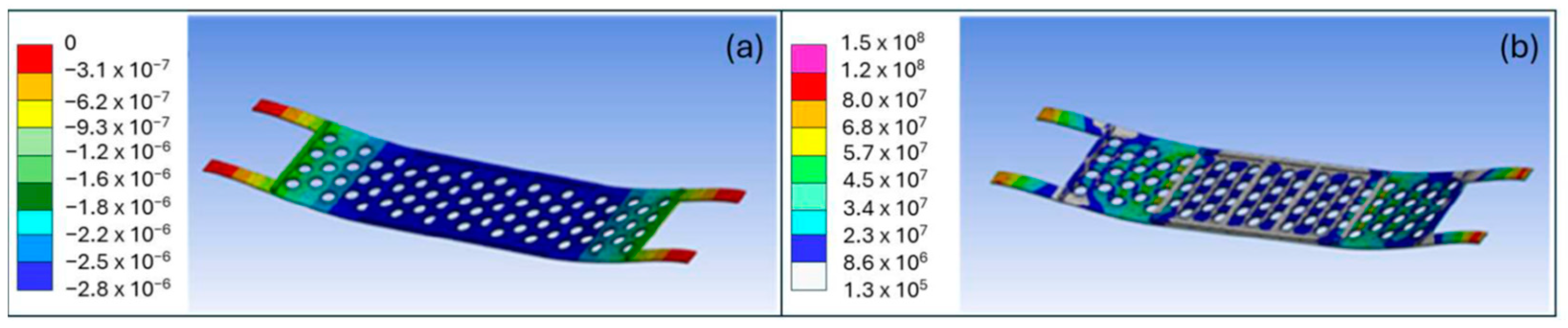
3. Results and Discussion

The pull-in voltage of fabricated switches was measured from the capacitance–voltage curve, finding the value of 43 ± 3 V. The fabricated fixed-fixed beams were modeled in the FEM ANSYS® Multiphysics (https://www.ansys.com/products/optics/multiphysics, accessed on 1 April 2024) environment. First, simulations for the calculation of the pull-in voltage were performed not taking into account the residual stress inside beams. A pull-in voltage of 29.5 V was calculated, which is significantly lower than the measured value. A residual stress was applied during simulations, and it was found that the measured pull-in voltage of 43 V is consistent with a residual stress of 48 MPa.
The static deformation of beams was modelled under the application of the measured pull-in voltage [Figure 2a]. When the pull-in voltage is applied, the central region of beams is electrostatically attracted towards the actuation pad. Consistently, the central region shows the maximum deflection, whereas the displacement gradually reduces along the intermediate and the spring sections, until it vanishes in the anchoring points. It is worth noting that the central plate of all beams is flat in the down state, likely due to two reasons: (1) the configuration of the beam-actuation pad allows the application of a central uniform electrostatic force and (2) the presence of the stiffer frame. The collapse of the central plate of the beam on the actuation pad is an important result because it allows us to maximize the ratio of capacitance in the down and up states, which is a figure of merit to measure the performance of capacitive RF MEMS switches. The nonuniform deflection due to the electrostatic actuation stretches the beam and induces an additional stress inside it [Figure 2b]. It is observable that the region of the central frame is characterized by the lowest values of stress, and the stress increases when moving from the central plate to the anchoring points, reaching the maximum values at the anchoring points.

Author Contributions

Conceptualization, A.P., J.I. and A.B.; methodology, A.P., G.T. and J.I.; software, G.T. and J.I.; resources, A.P., F.Q. and P.S.; writing—original draft preparation, A.P., J.I. and A.B.; writing—review and editing, A.P., J.I. and F.Q.; supervision, F.Q. and P.S. All authors have read and agreed to the published version of the manuscript.

Funding

This research received no external funding.

Institutional Review Board Statement

Not applicable.

Informed Consent Statement

Not applicable.

Data Availability Statement

No new data were created.

Conflicts of Interest

The authors declare no conflicts of interest.

References

  1. Deng, K.; Yang, F.; Deng, Z.; Wang, X.; Han, K. Analysis and design of a novel high capacitance ratio and low actuation voltage RF MEMS switch. Microsyst. Technol. 2021, 27, 2803–2813. [Google Scholar] [CrossRef]
  2. Bansal, D.; Bajpai, A.; Kumar, P.; Kaur, M.; Kumar, A. Effect of Stress on Pull-in Voltage of RF MEMS SPDT Switch. IEEE Trans. Electron Dev. 2020, 67, 2147–2152. [Google Scholar] [CrossRef]
  3. Persano, A.; Quaranta, F.; Capoccia, G.; Proietti, E.; Lucibello, A.; Marcelli, R.; Bagolini, A.; Iannacci, J.; Taurino, A.; Siciliano, P. Influence of design and fabrication on RF performance of capacitive RF MEMS switches. Microsyst. Technol. 2016, 22, 1741–1746. [Google Scholar] [CrossRef]
Figure 1. Typical SEM image of a fabricated RF MEMS switch. The labels l, r, and s are used to indicate the different sections of the beam and are equal to 65 µm, 100 µm, and 95 µm, respectively. The width of the beam is 100 µm.
Proceedings 97 00174 g001
Figure 2. Diagram of the deformation (a) and of the stress (b) that are induced by the electrostatic actuation of the beam.
Proceedings 97 00174 g002
Disclaimer/Publisher’s Note: The statements, opinions and data contained in all publications are solely those of the individual author(s) and contributor(s) and not of MDPI and/or the editor(s). MDPI and/or the editor(s) disclaim responsibility for any injury to people or property resulting from any ideas, methods, instructions or products referred to in the content.

