Abstract

Small Footprint Temperature Sensing NFC Tag †

1
INL—International Iberian Nanotechnology Laboratory, 4715-330 Braga, Portugal
2
Edilásio Carreira da Silva, 2430-069 Marinha Grande, Portugal
*
Author to whom correspondence should be addressed.
Presented at the XXXV EUROSENSORS Conference, Lecce, Italy, 10–13 September 2023.
Proceedings 2024, 97(1), 182; https://doi.org/10.3390/proceedings2024097182
Published: 12 April 2024

Abstract

:
Smart NFC tags are seeing many interesting applications and can benefit from further miniaturization. A passive temperature sensing tag with 5.1 mm diameter is demonstrated, comprising a thin-film microfabricated antenna and an NFC chip. The microantenna/coil comprises two 15 µm-thick electroplated copper layers embedded in SU-8, withstanding the soldering process of a BGA NFC IC. The µ-antenna design challenge is to miniaturize while minimizing performance impairment (inductive-coupling distance), while the micromachining process is very dependent on topography propagation. Fabricated coils were successfully characterized (2.32 µH inductance; 13.76 MHz self-resonance) and temperature was read (after assembly) with a mobile phone at distances of up to 7 mm.

1. Introduction

Battery-less Near Field Communication (NFC) smart sensing tags have seen significant attention in recent years, especially for biomedical applications, with several devices proposed, typically with diameters above 10 mm, and fabricated using flexible substrates [1]. An example of a small form factor device is the pressure-, temperature-, and humidity-sensing tag, targeting packaged food monitoring (25 × 25 mm2, <1 mW power consumption) [2]. In this work, we aim to further miniaturize an NFC tag with sensing capabilities in order to enable its overmolding and integration into injected parts. In order to do so, a µ-antenna was fabricated using planar process microfabrication techniques that allow for coils with trace width and spacing below 20 µm, and integrated with a commercial NCF IC (size 2.51 × 2.51 × 0.5 mm3) that includes a temperature sensor. Its small form-factor (5.1 mm diameter) enables integration into injection-molded parts, making it a versatile, highly convenient, and non-intrusive solution for precise monitoring of temperature levels. The main challenges are the design—the trade-off between miniaturization and performance, and the microfabrication—the difficulty of patterning high aspect ratio features and vias on 10–25 µm-thick polymeric layers (photoresist and SU-8).

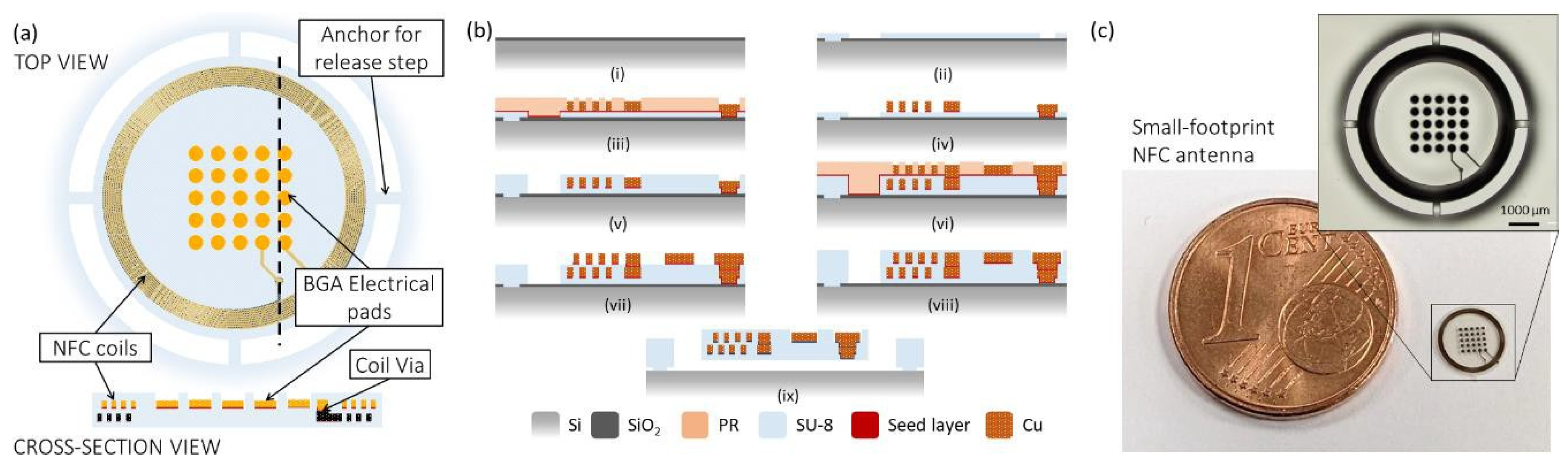
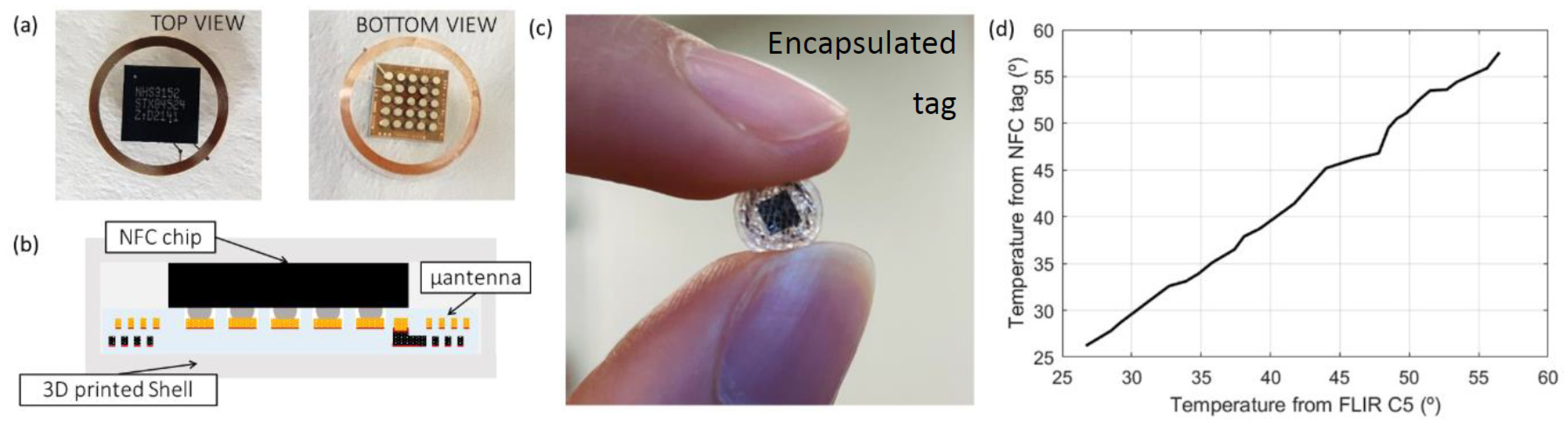
2. Miniaturized Temperature Sensing Tag: µ-Antenna Fabrication and NFC IC Assembly

The device comprises a thin-film (50 µm thick) µ-antenna consisting of a two-layer electroplated copper coil (eight turns each) embedded in SU-8, with 5.1 mm diameter and BGA compatible pads. The microfabrication process (Figure 1b) starts with deposition and patterning of SiO2 (sacrificial release layer), followed by a 5 µm SU-8 layer which acts as the device bottom flexible base. The active features (coil) are two layers of 15 µm electroplated copper, separated by 10 μm of SU-8 (with patterned vias for copper connections). A 20 μm-thick layer of SU-8 is finally patterned, leaving the BGA copper contacts exposed. The devices are then released using hydrogen fluoride (HF) vapor etch. The NFC IC (NHS3152) with integrated temperature sensor (and a resistive network sensing-interface) is soldered to the flexible µ-antenna and enclosed in a 3D-printed shell (Figure 2).

3. Experimental Results and Discussion

Prior to soldering and encapsulation, the µ-antennas were experimentally characterized (2.32 µH). The micromachining process was deemed successful based on the coil resistance of 12.2 Ω and resonance frequency of 13.76 MHz (extracted from the measurements). After encapsulation with 3D filament printing, the temperature data and tag ID were successfully read with a smartphone NFC reader at distances of up to 7 mm. Using a ceramic hotplate, the tag was heated from room temperature to approximately 55 °C and its measurements were compared to the readings from a FLIR C5 Thermal Camera (Figure 2d). A microfabricated thin-film piezoresistive pressure sensor integrated with the µ-antenna is currently being pursued using the same footprint, targeting monitoring of ambient air pressure variations.

Author Contributions

Conceptualization, R.A.D., G.R., M.M. and A.C.; methodology, F.S.A., J.F., R.A.D. and I.S.G.; microfabrication, J.P. and J.F.; writing, J.P. and I.S.G.; assembly and experimental characterization, M.M. and J.P. All authors have read and agreed to the published version of the manuscript.

Funding

This research was supported by the project IMOCO4.E—Intelligent Motion Control under Industry4.E, funded by the Electronic Component Systems for European Leadership Joint Undertaking, under Grant Agreement n°101007311 and by the Portuguese Foundation for Science and Technology (FCT).

Institutional Review Board Statement

Not applicable.

Informed Consent Statement

Not applicable.

Data Availability Statement

Raw data is available by request.

Conflicts of Interest

The authors declare no conflicts of interest.

References

  1. Kang, S.-G.; Song, M.-S.; Kim, J.-W.; Lee, J.W.; Kim, J. Near-Field Communication in Biomedical Applications. Sensors 2021, 21, 703. [Google Scholar] [CrossRef] [PubMed]
  2. Nguyen, T.-B.; Tran, V.-T.; Chung, W.-Y. Pressure Measurement-Based Method for Battery-Free Food Monitoring Powered by NFC Energy Harvesting. Sci. Rep. 2019, 9, 17556. [Google Scholar] [CrossRef] [PubMed]
Figure 1. (a) Schematic representation of NFC μ-antenna, (b) main micromachining process steps, and (c) photograph and microscope image (close-up) of the fabricated devices. Microfabrication includes (i) SiO2 deposition on silicon wafer, (ii) SiO2 patterning and SU-8 lithography (iii) Seed layer deposition, thick resist lithography and copper electroplating, (iv) resist removal (v) SU-8 lithography, (vi) thick resist lithography and copper electroplating, (vii) resist removal, (viii) SU-8 lithography and (ix) HF vapor release.
Proceedings 97 00182 g001
Figure 2. (a) Temperature sensing tag before encapsulation, (b) encapsulation schematic, (c) picture of encapsulated tag, and (d) NFC tag temperature measurements against thermal camera readings.
Proceedings 97 00182 g002
Disclaimer/Publisher’s Note: The statements, opinions and data contained in all publications are solely those of the individual author(s) and contributor(s) and not of MDPI and/or the editor(s). MDPI and/or the editor(s) disclaim responsibility for any injury to people or property resulting from any ideas, methods, instructions or products referred to in the content.

