Article

Analysis of Tempering Effects on LDS-MID and PCB Substrates for HF Applications

1
Institute for Micro Integration (IFM), University of Stuttgart, Allmandring 9b, 70569 Stuttgart, Germany
2
Hahn-Schickard, Allmandring 9b, 70569 Stuttgart, Germany
*
Author to whom correspondence should be addressed.
J. Manuf. Mater. Process. 2023, 7(4), 139; https://doi.org/10.3390/jmmp7040139
Submission received: 16 June 2023 / Revised: 27 July 2023 / Accepted: 1 August 2023 / Published: 3 August 2023

Abstract

:
Mechatronic Integrated Devices or Molded Interconnect Devices (MID) are three-dimensional (3D) circuit carriers. They are mainly fabricated by laser direct structuring (LDS) and subsequent electroless copper plating of an injection molded 3D substrate. Such LDS-MID are used in many applications today, especially antennas. However, in high frequency (HF) systems in 5G and radar applications, the demand on 3D circuit carriers and antennas increases. Electroless copper, widely used in MID, has significantly lower electrical conductivity compared to pure copper. Its lower conductivity increases electrical loss, especially at higher frequencies, where signal budget is critical. Heat treatment of electroless copper deposits can improve their conductivity and adhesion to the 3D substrates. This paper investigates the effects induced by tempering processes on the metallization of LDS-MID substrates. As a reference, HF Printed Circuit Boards (PCB) substrates are also considered. Adhesion strength and conductivity measurements, as well as permittivity and loss angle measurements up to 1 GHz, were carried out before and after tempering processes. The main influencing factors on the tempering results were found to be tempering temperature, atmosphere, and time. Process parameters like the heating rate or applied surface finishes had only a minor impact on the results. It was found that tempering LDS-MID substrates can improve the copper adhesion and lower their electrical resistance significantly, especially for plastics with a high melting temperature. Both improvements could improve the reliability of LDS-MID, especially in high frequency applications. Firstly, because increased copper adhesion can prevent delamination and, secondly, because the lowered electrical resistance indicates, in accordance with the available literature, a more ductile copper metallization and thus a lower risk of microcracks.

1. Introduction

As the roll-out of 5G continues and the usage of mmWave radar increases, an ever increasing amount of high frequency systems are needed and drives new and diverse applications [1]. Those necessitate new restrictions on available space, performance, and cost [2]. While standard HF PCB technology is mainly used for manufacturing such HF devices at lower frequencies, it often lacks the capability of high performance HF Systems in a sufficiently small form factor. Moreover, their manufacturing tolerances exceed the acceptable limits to a reasonable price [3]. One alternative is the employment of MID. Especially LDS-MID combine complex 3D bodies with a proven technology for applying circuitry on those 3D bodies at a reasonable price.
LDS-MID are produced by a manufacturing process described in detail by Franke et al. [4]. First, a circuit carrier is manufactured by injection molding a special thermoplastic containing a laser activatable additive (LDS additive). To generate a circuit pattern and to drill vertical interconnect accesses, an infrared laser is used. The laser activates the LDS additive and roughens the plastics surface to promote copper adhesion in the subsequent metallization step. Afterwards a cleaning process removes the laser debris from the structured LDS-MID. This step can be performed by ultrasonic supported wet chemical cleaning, by water jet cleaning, or by carbon dioxide snow jet cleaning [5]. After cleaning, the LDS-MID are metallized by electroless copper plating and an appropriate surface finish. Finally, passive and active surface-mount devices are assembled.
LDS-MID are widely used as antennas in mobile devices up to 6 GHz [4]. But, concepts are also developed to employ LDS-MID in base-stations [6,7]. Also higher performing and miniaturized antennas for surface mounting are available, like GPS antennas from the company Molex LLC (Lisle, IL, USA) [8]. Moreover, demonstrators for LDS-MID based mmWave applications were also presented in the literature [9,10,11,12,13,14,15]. Glise et al. demonstrated the usability of LDS-MID for manufacturing high quality substrate integrated waveguide filters around 40 GHz [9] and Laur et al. showed the usability of LDS-MID for manufacturing self-biased circulators at around 30 GHz [10]. Friedrich et al., on the other hand, showed the applicability of LDS-MID for manufacturing substrate filled horn-antennas at frequencies of around 24 GHz and 77 GHz [11,12,13]. In regard to integration, further design studies on miniaturization of coplanar waveguides in LDS-MID technology and integration of LDS-MID antennas in handheld devices for mmWave coverage have been published by Seewald et al. [14,15].
In addition to the properties of substrate and design, the performance of a high frequency (HF) system is largely determined by the properties of its metallization. Electroless deposited copper, as used in LDS-MID, has an increased electrical resistance compared to pure copper. This is due to a fine grained structure and varying contents of organic impurities and hydrogen embedded in voids. It can be categorized in four different types, with increasing degrees of impurity from type I to IV [16]. The increased electrical resistance affects the induced losses in HF circuitry with rising frequencies even more as in direct current applications. The reason is the skin effect, which leads to a concentration of the electric current in a thinner layer on the metal surface as frequencies increase [17]. The higher current density leads to more electrical losses, which is further amplified by the roughness of the metallization. These losses can be reduced if the electrical resistance of the metallization can be improved.
Different publications showed that the mechanical and electrical properties of electroless deposited copper can be significantly improved by tempering processes [16,18,19,20,21,22,23,24]. During these processes the amount of hydrogen within the electroless copper decreases by molecular diffusion. Furthermore, the grain boundaries move and the grain size increases, while the decreasing amount of hydrogen mainly enhances the ductility of the material, the increasing grain size improves the electrical resistance of the material.
Moreover, changes on the interface between copper and polymer substrate and improved adhesion of electroless copper after tempering processes were reported in [20,21,25]. The main theory is, that a copper oxide layer is growing at the interface between copper and substrate and induce an increased chemical bond, strengthening the interface. This increase in adhesion is of additional interest for HF system reliability, since reduction in the metallization roughness mostly decreases the adhesion. Those processes of hydrogen diffusion, grain growth, and interface oxidation also take place during specimen storage at room temperate and in an air atmosphere—although at a lower rate and absolute level [24,26]. Thus, a tempering process should be used to bring the electroless copper into a stabilized state. For LDS-MID, the effects of heat treatments on the adhesion strength and electrical conductivity as well as on the dielectric properties of the plastic substrates, have not yet been described in the scientific literature. This paper provides insights on heat treatments of various LDS-MID and HF PCB substrates regarding these properties. Effects of different process parameters, like holding temperature and time, tempering in air or in a vacuum, and heating rate were analyzed. Additionally, different metallization surface finishes were used.

2. Materials and Methods

2.1. Substrate Materials and Layout

In this paper, three different LDS-MID materials were investigated: Xantar LDS 3760, Tecacomp LCP LDS black 4107, and Tecacomp PEEK LDS black 1047045 (Table 1). Xantar LDS 3760 (PC LDS) [27] is based on the cheap commodity plastic polycarbonate (PC) and was used to investigate if tempering processes at lower temperatures are beneficial for low cost applications. Tecacomp LCP LDS black 4107 (LCP LDS) [28] is based on a liquid crystal polymer (LCP) and filled with a high amount of a mineral filler. Tecacomp PEEK LDS black 1047045 (PEEK LDS) [29] is based on poly-ether-ether-ketone (in the following PEEK LDS) and is modified with the same mineral filler as used in LCP LDS. As a reference material, the thermoset-based PCB material Rogers RO4350b [30] and the polytetrafluoroethylene (PTFE) based material TSM-DS3 [31] from Taconic were investigated (Table 1).
The LDS-MID substrates were injection molded plates with a size of 37 × 37 mm2 and a thickness of 1.5 mm. The PCB substrates had a size of 40 × 40 mm2 and a thickness of 1.5 mm. The layout used for the test specimens is shown in Figure 1. It included a meander layout of 0.75 m length, with a signal track and isolation width of about 0.1 mm. For accurate measurement of the electrical resistance, a special pad geometry for four-wire measurement was used. Additionally, 16 circular metallization pads with a diameter of 0.9 mm for hot-bump-pull (HBP) tests were included. For dielectric measurements unmetallized specimens were used.

2.2. Metallization and Surface Finishes

The properties of the LDS-MID metallization are affected by the laser parameters, e.g., pulse energy, pulse frequency, scanning speed and pulse pitches, the cleaning process prior to the electroless copper metallization, and the metallization process parameters. Depending on the substrate material and laser parameters, the structuring process causes ablation and a kind of micro-roughend and foamed layer on top of the bulk plastic. For standard applications, an ultrasonic supported wet chemical cleaning process is used. In combination, this results in a rough metallization layer, which is penetrated with plastic near the interface. This is beneficial due to the strong interlocking of plastic and copper, but increases the roughness of the metallization. However, when the laser parameters are adjusted accordingly and a carbon dioxide snow jet cleaning or water jet cleaning process is employed prior to metallization, the plastic surface is planarized and the applied metallization is smoother [5]. In Figure 2, examples of both kinds of metallization layers are shown on a PEEK LDS substrate in comparison to a metallization on a RO4350b substrate. In this study, the experiments were conducted on optimized LDS-MID with a smooth metallization layer. It can be assumed that the chemical processes within the metallization and the interface between copper and thermoplastic will take place regardless of the complexity of the metallization morphology. Consequently changes in electrical resistance of a smooth and optimized metallization can be transferred to the standard metallization.
Three different metallization stack-ups were used as surface finish. The standard surface finish for LDS-MID is Ni/Au (electroless nickel, immersion gold) with a nickel diffusion barrier of about 6–7 µm and a thin gold layer of about 0.1–0.2 µm. As alternative an Ag (immersion silver) finish with 0.1–0.2 µm thickness and a Pd/Au (electroless palladium, immersion gold) finish with 0.1–0.2 µm palladium and 0.1–0.2 µm gold were used. Those two surface finishes show a better fine pitch capability compared to Ni/Au due to their low thickness. Additionally, Ag and Pd/Au are free from nickel, which is avoided in HF applications because of the high losses caused by its low electrical conductivity.
Contrary to that, the metallization on PCBs is different. It consists of copper with higher purity due to its manufacturing by galvanic deposition or rolling. Furthermore, the edges are much sharper due to the subtractive structuring process. In this case, the copper foil bonded to the substrates was about 15 µm thick. The surface finishes on the HF PCBs were applied with the same processes as for the LDS-MID substrates.

2.3. Setup of Tempering Experiments

The tempering experiments were performed on a RLKV 40/1 lamination press from Lauffer Maschinenfabrik GmbH, (Horb am Neckar, GER). No pressure was applied. The advantage of using the press compared to a conventional oven was the possibility of tempering in a vacuum.
  • Experiment 1 was carried out to investigate the effects of different heating rates on the LDS-MID substrates. The heating was performed at three different heating rates of 1 K/min, 3 K/min, and 10 K/min. The materials LCP LDS and PEEK LDS were held at 200 °C for two hours and the PC LDS was hold at 90 °C for four hours. The investigated surface finish was Ni/Au and the experiment was conducted in a vacuum. The temperature of 200 °C was chosen to match the temperature used in [16]. A value of 90 °C for PC LDS was chosen to be slightly higher than its glass transition temperature.
  • Experiment 2 investigated the influence of tempering on different surface finishes. Pure copper metallization was used as well as copper metallization with Ni/Au, Ag and Pd/Au finishes on PEEK LDS, RO4350b and TSM-DS3 substrates. The heating rate was set to 10 K/min and the temperature was held at 200 °C for up to two hours. The presence of air during tempering was compared to tempering in a vacuum. Additionally, a box oven was used to temper PEEK LDS specimens with Ni/Au and Ag surface finish at 200 °C. The samples were placed directly into the oven, preheated to 200 °C, and removed after 2 h.
  • Experiment 3 investigated the effect of longer tempering time and lower temperature on LDS-MID materials. The specimen were metallized with copper and Pd/Au surface finish. LCP LDS and PEEK LDS substrates were tempered for two, four and eight hours at temperatures of 120 °C and 200 °C, respectively. The PC LDS substrates were tempered for four, eight and sixteen hours at 90 °C. The heating rates for all substrates were set to 10 K/min.

2.4. Characterization of Adhesion Strength by Hot-Bump-Pull Test

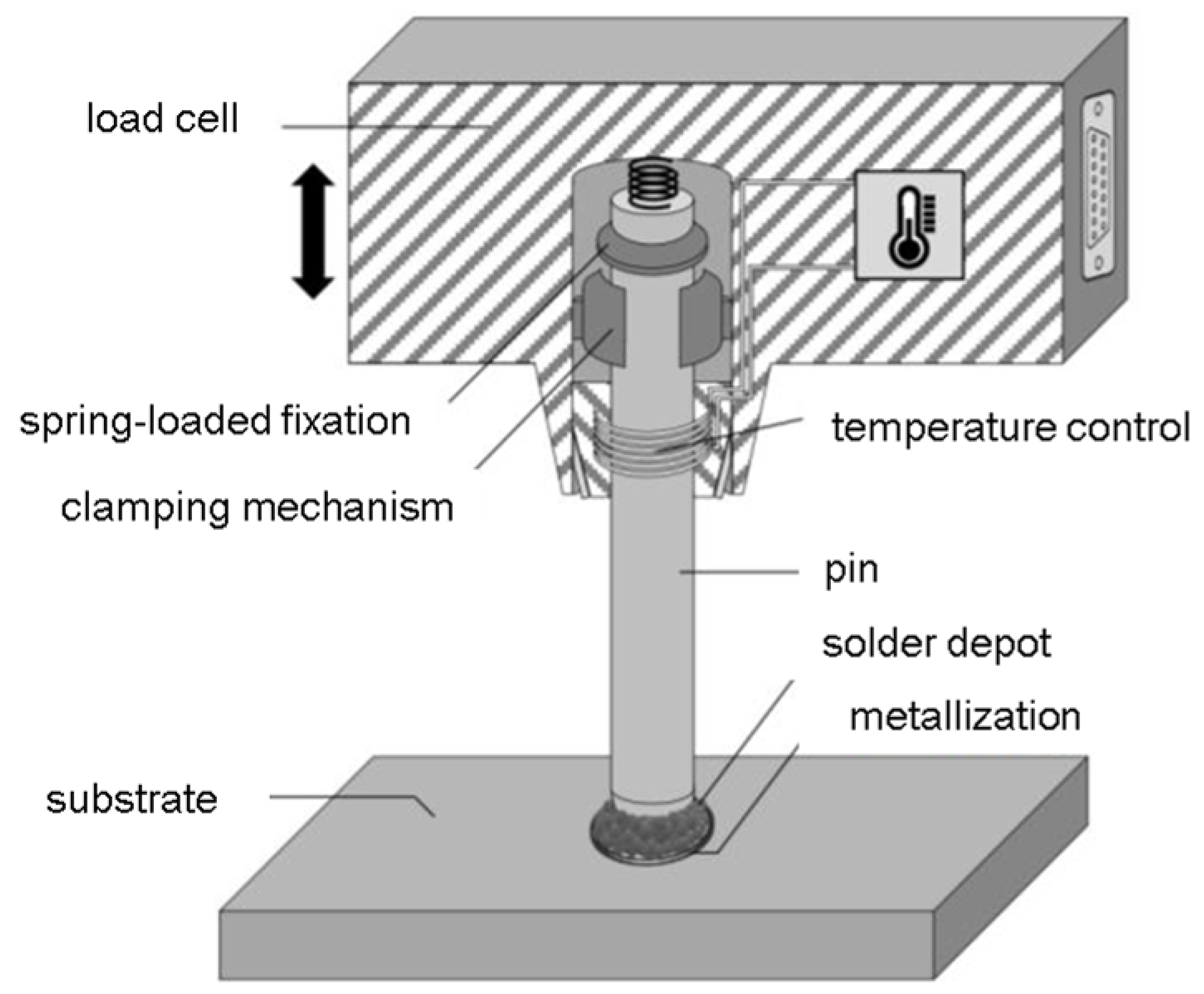
The adhesion strength of the metallization was determined by a hot-bump-pull test on a Nordson Dage 4000Plus bond testing unit from Nordson Corp. (Westlake, OH, USA) (Figure 3). This method was applied because a standard peel test as commonly used in PCB technology is not applicable to the electroless deposited copper metallization on LDS-MID due to its brittleness. First, a copper pin is soldered with a low temperature tin-bismuth solder (type Sn42Bi58 with a melting temperature of 138 °C) onto the circular pads of the specimen. For all materials except PEEK LDS, including the reference materials, the same temperature profile was used with a peak temperature of 160°C. This temperature was chosen as it is at the lower end of the peak soldering temperature range of this particular solder. The main reason for this is to minimize the thermal impact on the material, as excessive heat could damage the interface between metallization and substrate for some materials. For PEEK LDS a profile with higher peak temperature and a longer holding time is needed, as defined in Table 2, because of the enhanced thermal conductivity of this material. After cooling, a pull force was applied and the metallization was pulled of the substrate. Each measurement set consisted of 5 measurements each.

2.5. Dielectric Characterization by Capacitance Cell Measurement

The characterization of the dielectric material properties was performed by the method of parallel plate capacitor measurement. To analyze the dielectric material, it was clamped between two electrodes. For the measurements the test fixture 16453A and the E4991A Impedance/Material Analyzer from Keysight Technologies Inc. (Colorado Springs, CO, USA) were used. With this method, it is possible to measure the dielectric constant Dk and the dielectric loss factor Df up to 1 GHz.

2.6. Measurement of Electrical Resistance

To determine the electrical resistance of the meanders a 34410A 6.5 Digit Multimeter from from Keysight Technologies Inc. (USA) and the four wire measurement method were used. For each set of experiment two meanders were measured and for each measurement the measurement tips were set down three times and the results were averaged.

3. Results

3.1. Initial Characterization of Adhesion Strength

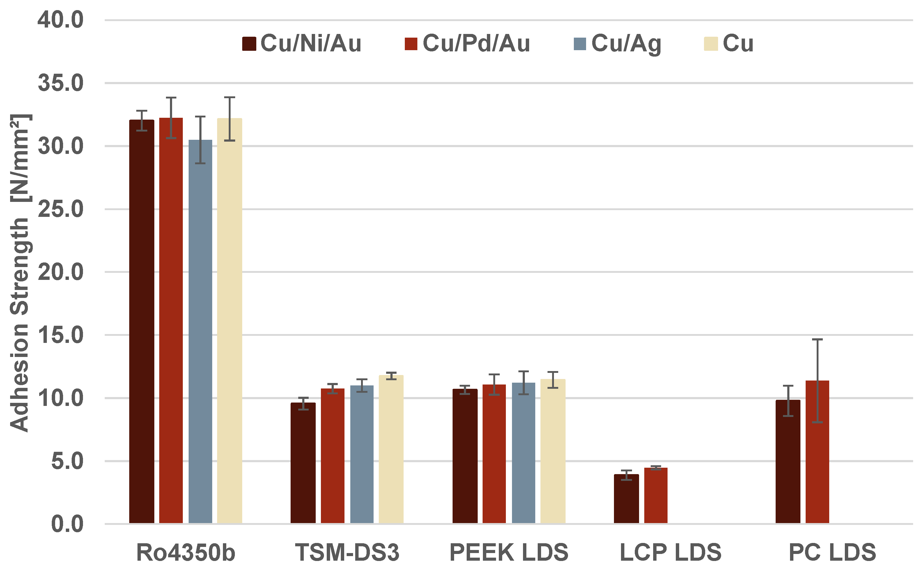
The initial adhesion strength of the metallization on all materials is depicted in Figure 4. For LCP LDS and PC LDS the adhesion strength was only measured for Cu/Ni/Au and Cu/Pd/Au. For RO4350b, TSM-DS3 and PEEK LDS additional adhesion strength data for pure copper metallization and Cu/Ag were generated. The highest adhesion strength with values above 30 N/mm² shows Rogers RO4350b. The adhesion strength on TSM-DS3, PEEK LDS, and PC LDS is in the range between 9 N/mm² and 12 N/mm². On LCP LDS the overall lowest adhesion strength with values of about 4 N/mm² can be seen. In Figure 4, the standard deviations of the measurements are also shown. While the standard deviations for TSM-DS3, PEEK LDS, and LCP LDS are comparable and consistent to each other, the standard deviation for RO4350b and PC LDS is significantly higher. For RO4350b the mean values are 3 times higher, thus causing a higher standard deviation. For PC LDS the higher variation in adhesion strength is probably caused by the low thermal stability of the material itself. During the soldering process of the metal pin for hot-bump-pull tests the material can be damaged by the temperature exposure, thus leading to a higher variation in adhesion strength.

3.2. Initial Characterization of Electrical Resistance

In Figure 5, the results of initial electrical resistance measurements of all substrates are depicted. The metallizations on PCB substrates exhibits the lowest resistance, due to their higher metallization thickness, wider transmission lines and lower specific resistance. For LDS-MID metallization, the lowest overall resistance can be observed for LCP LDS, followed by PC LDS and PEEK LDS. This corresponds to the cross-section area of the copper tracks, see Table 3. Also, a higher impact of the metallization surface finishes on the electrical resistance can be seen for the LDS materials, due to the overall lower metallization thickness and higher roughness of LDS-MID metallizations.

3.3. Initial Characterization of Dielectric Properties

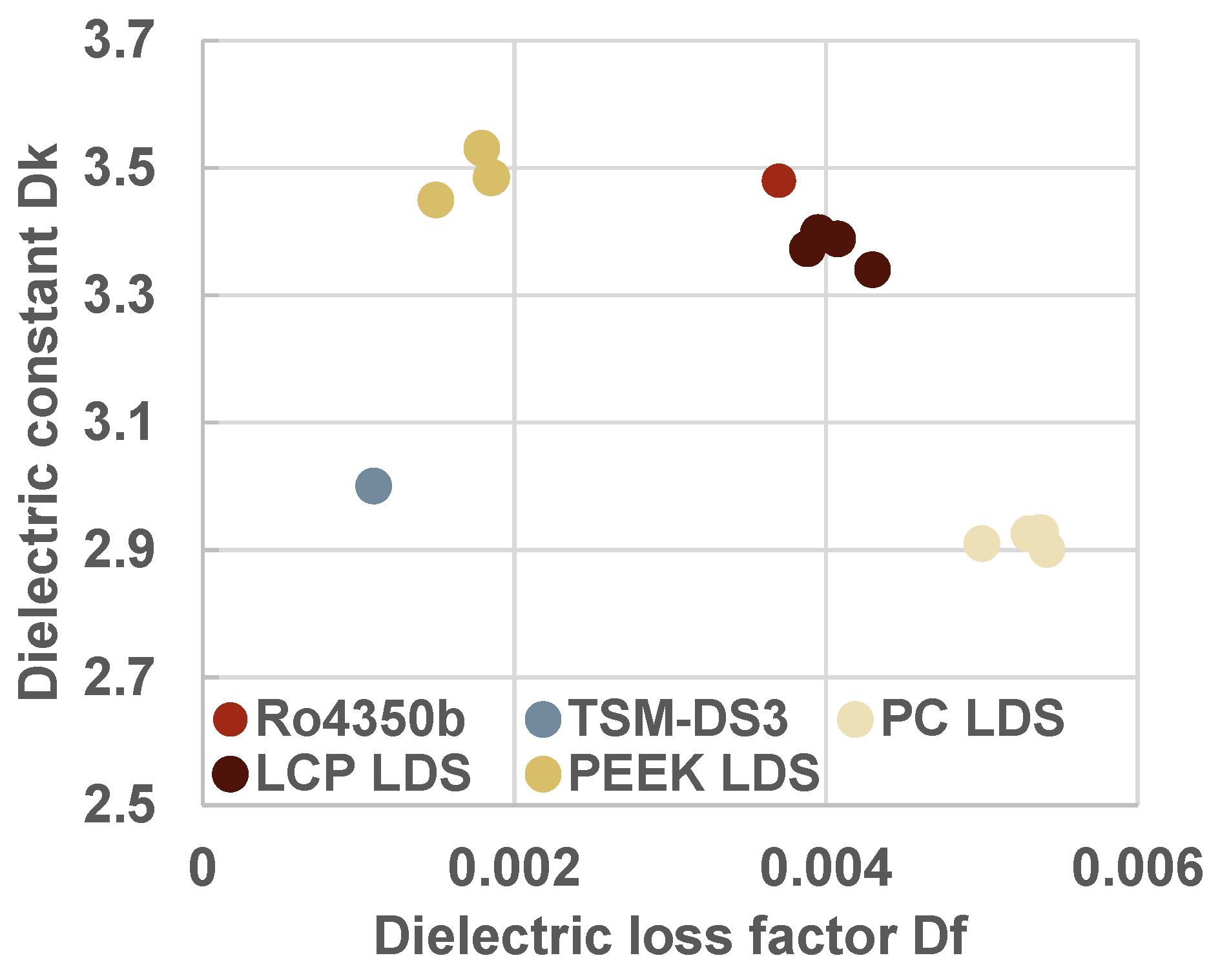
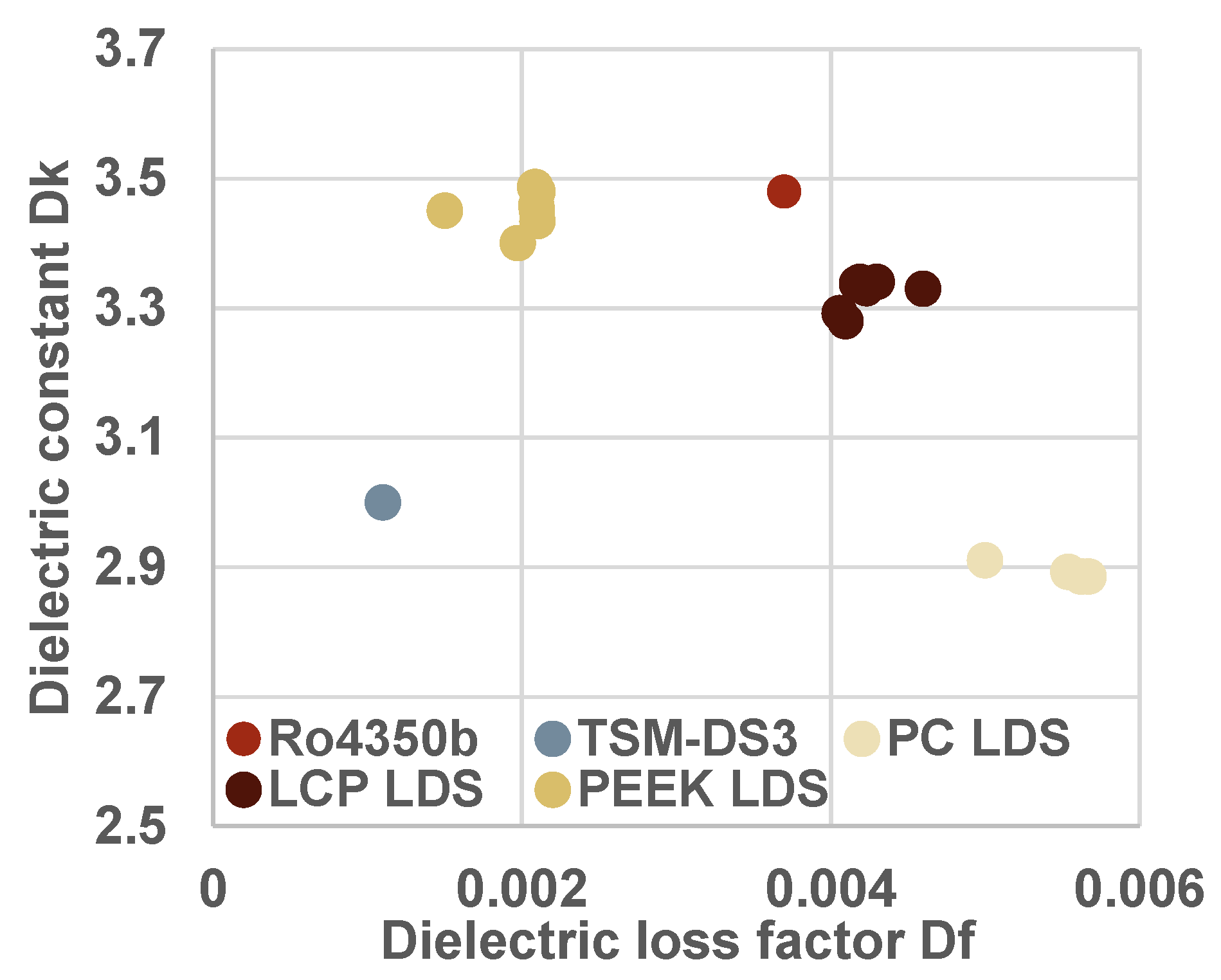
Table 4 shows the results on Dk and Df for all three LDS-MID materials and the datasheet values of RO4350b [30] and TSM-DS3 [31]. PEEK LDS is found to have the highest Dk value of 3.4 at 1 GHz, but also offers the lowest dielectric loss Df of 0.0025 at 1 GHz of all LDS materials analyzed. LCP LDS follows right behind PEEK LDS regarding the Dk with a value of 3.3 and a Df value of 0.005. The unfilled PC LDS shows the lowest Dk of about 2.9. and a DF of 0.006. The data shown are mean value of at least 3 measurements. For TSM-DS 3 [31] the data sheet indicates a Dk of 3.0 ± 0.04 over a broad range of frequencies and a Df of 0.0014 at 10 GHz. Rogers RO4350b [30] shows a Dk of 3.48 ± 0.05 and a Df of 0.0037 at 10 GHz. Therefore, it can be concluded, that the LDS-MID materials perform similar to medium to high price HF PCB materials.

3.4. Experiment 1: Effects of Different Heating Rates

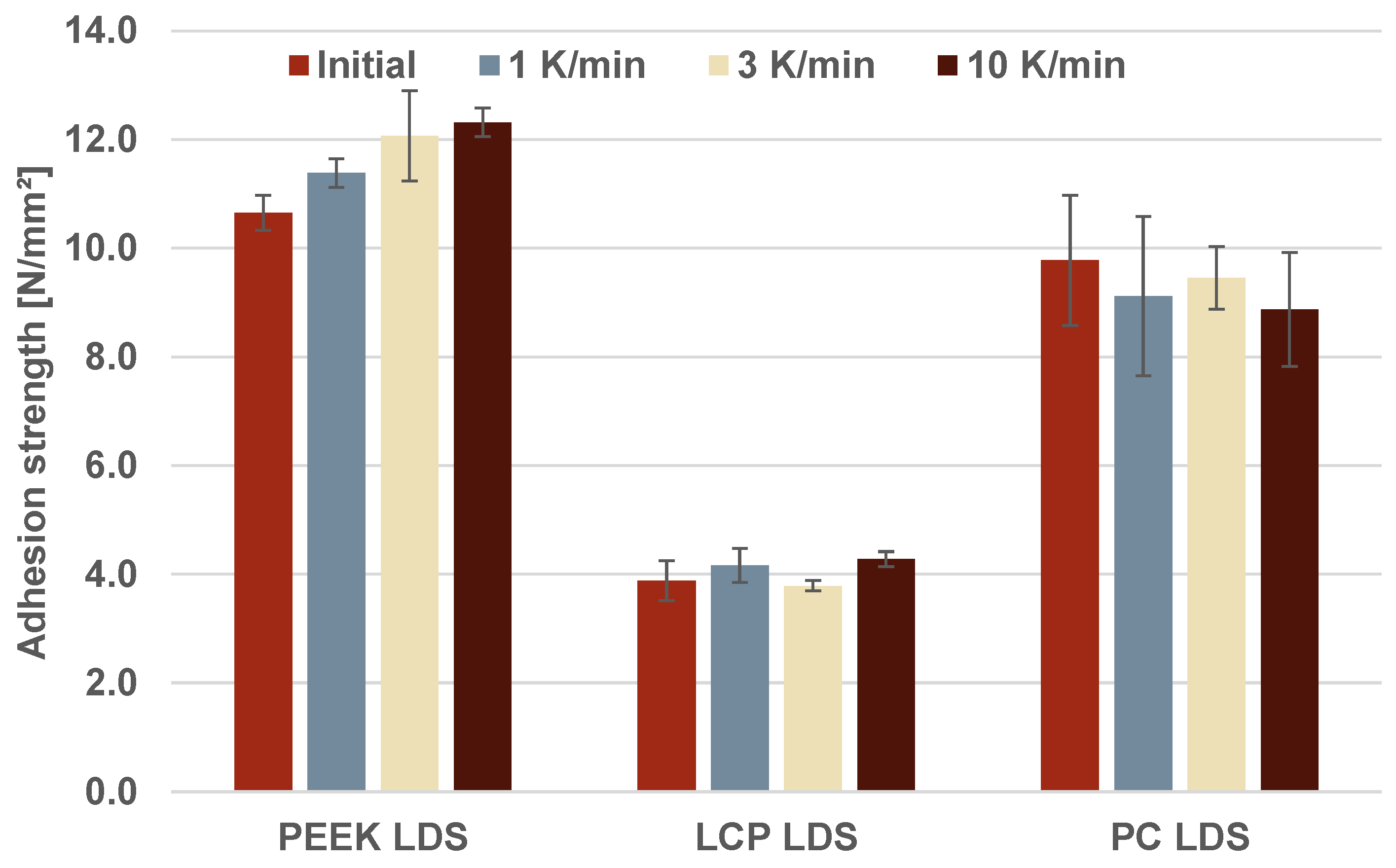
The results of the tempering experiments regarding the adhesion strength are depicted in Figure 6. The metallization on PEEK LDS with Ni/Au finish shows a significant increase in adhesion strength for different heating rates with a positive correlation between adhesion strength improvement and heating rate. For LCP LDS no significant increase is observed, except for a heating rate of 10 K/min. The tempering of PC LDS shows no significant effect on the adhesion strength. This may be caused by the lower tempering temperature applied.
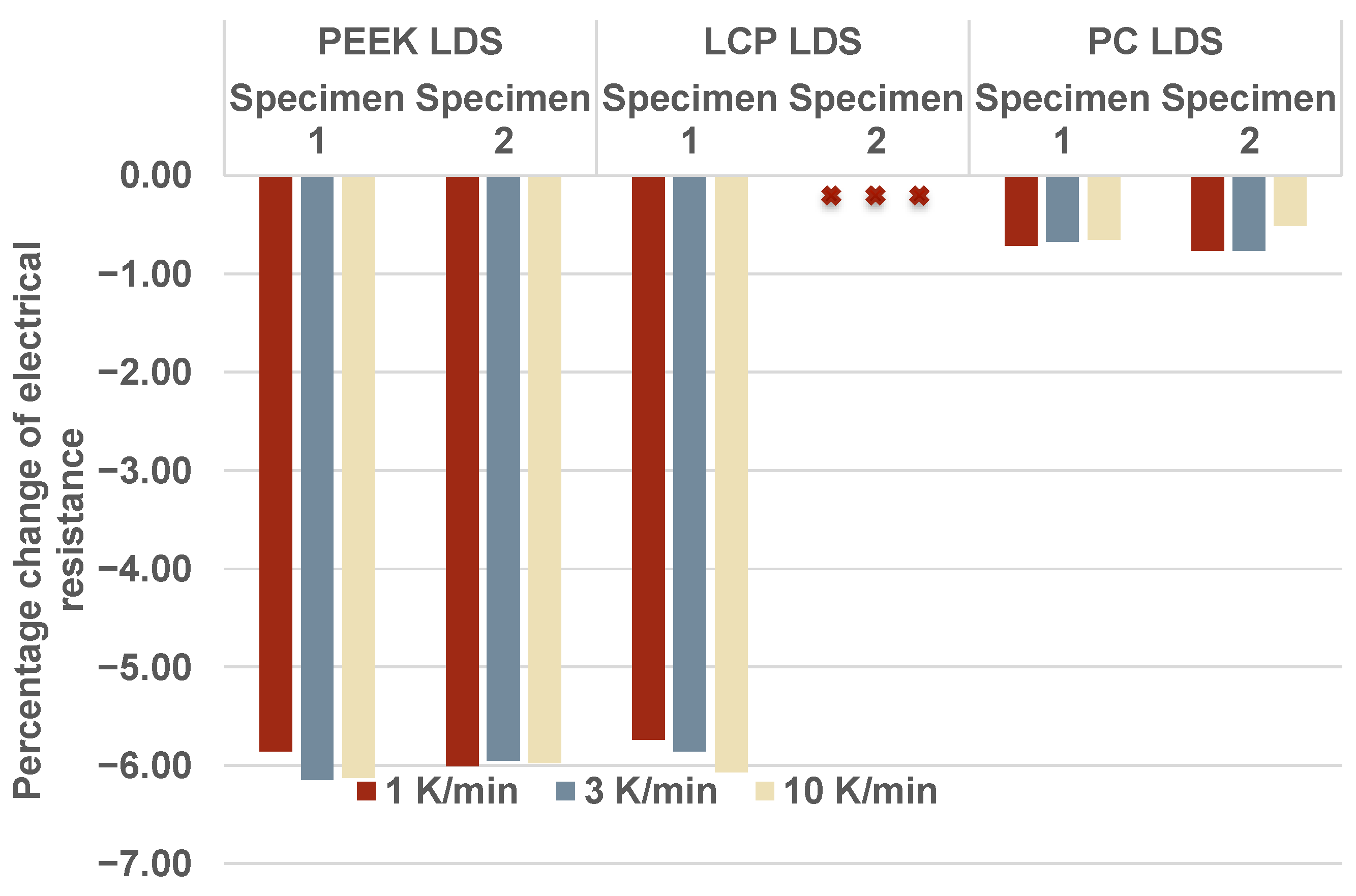
The electrical resistance of the meander drops for every variation of heating rate, as shown in Figure 7. The plot shows that the decrease in electrical resistance on PEEK LDS and LCP LDS is similar and reaches approximately 6% of the initially measured values. For LCP LDS one specimen in each test failed and no electrical resistance is recorded (red cross in Figure 7). For the meander on PC LDS no significant change can be observed, which can be explained by the lower tempering temperature applied. The measurements of dielectric properties show only minor changes in dielectric constant Dk and dielectric loss Df for all investigated substrates (Figure 8).

3.5. Experiment 2: Effects of Different Metallization Surface Finishes and Tempering Atmosphere

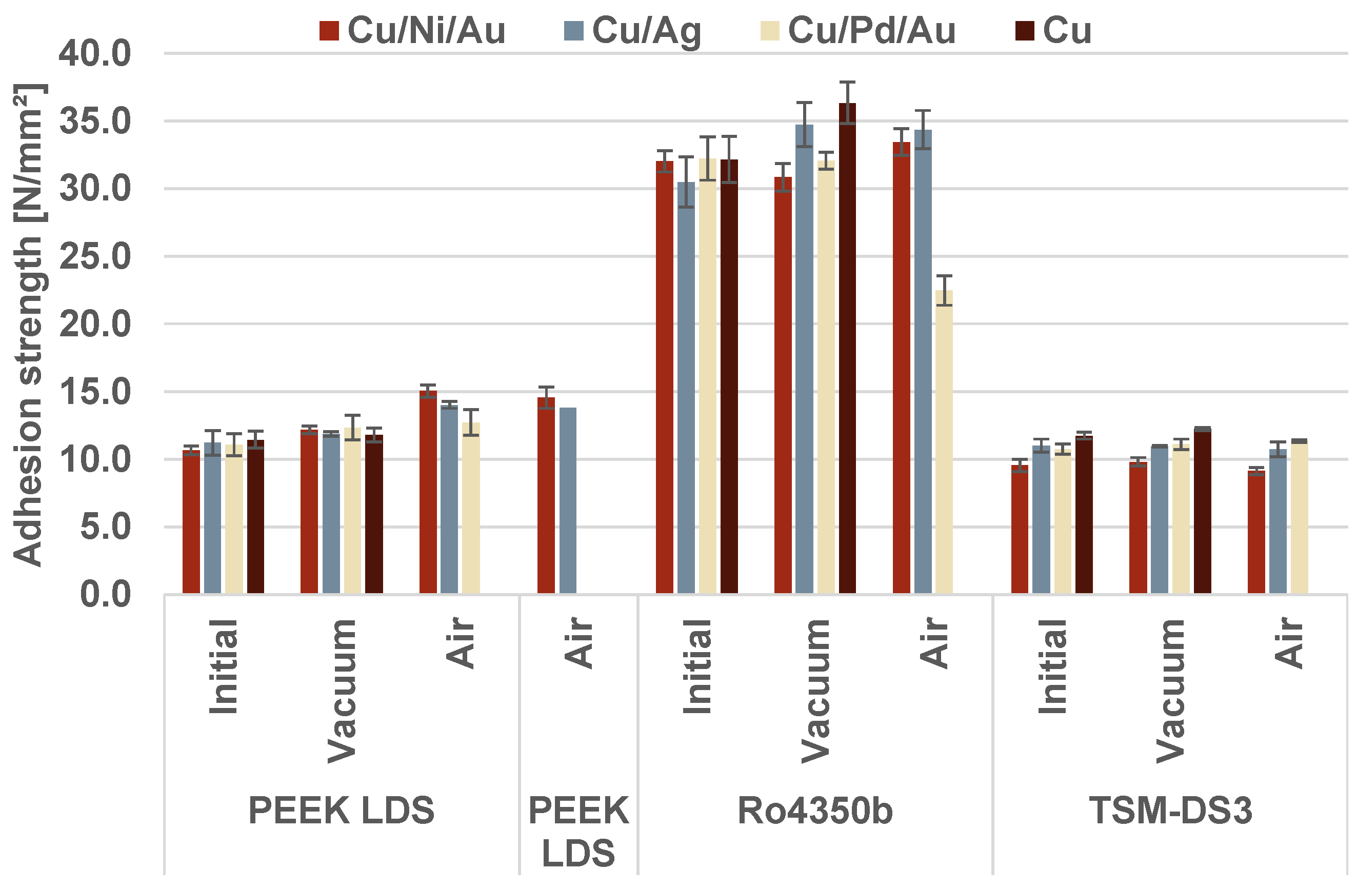
The aim of this experiment is to investigate the influence of vacuum during tempering on the adhesion strength and electrical resistance of the metallization for different surface finishes. The results regarding the adhesion strength are shown in Figure 9. For RO4350b substrates with Cu/Ni/Au metallization tempering in vacuum decreases the adhesion strength by 3.7%, while tempering in air atmosphere increases it by 4.5%. For Cu/Pd/Au the applied vacuum shows no significant influence, but tempering in air atmosphere decreases the adhesion strength about 30%. Regarding adhesion strength of copper metallization and tempering in a vacuum as well as adhesion strength of Cu/Ag for both variations of atmosphere the tempering increases the adhesion strength between 12.5% and 14.0%. For the metallization of TSM-DS 3 substrates only slight changes of the adhesion strength can be observed.
PEEK LDS substrates show the overall most significant changes for all investigated metallizations (Figure 9). Only tempering of copper metallization in a vacuum causes no significant change. As discussed above, an increase in adhesion strength could be caused by oxidation of the copper at the interface to the substrate. For Cu/Ni/Au metallization in Figure 9 an increase in adhesion strength of about 14.1% for tempering in a vacuum, 41.1% for tempering in air, and 36.7% for tempering in the box oven is depicted. The adhesion strength for Cu/Pd/Au and Cu/Ag metallizations increases by about 11.4% and 5.8%, respectively, for tempering in a vacuum and for tempering in air by 31.3% and 25.0%, respectively. The additional tests using a box oven confirm the significant increase in the adhesion strength.
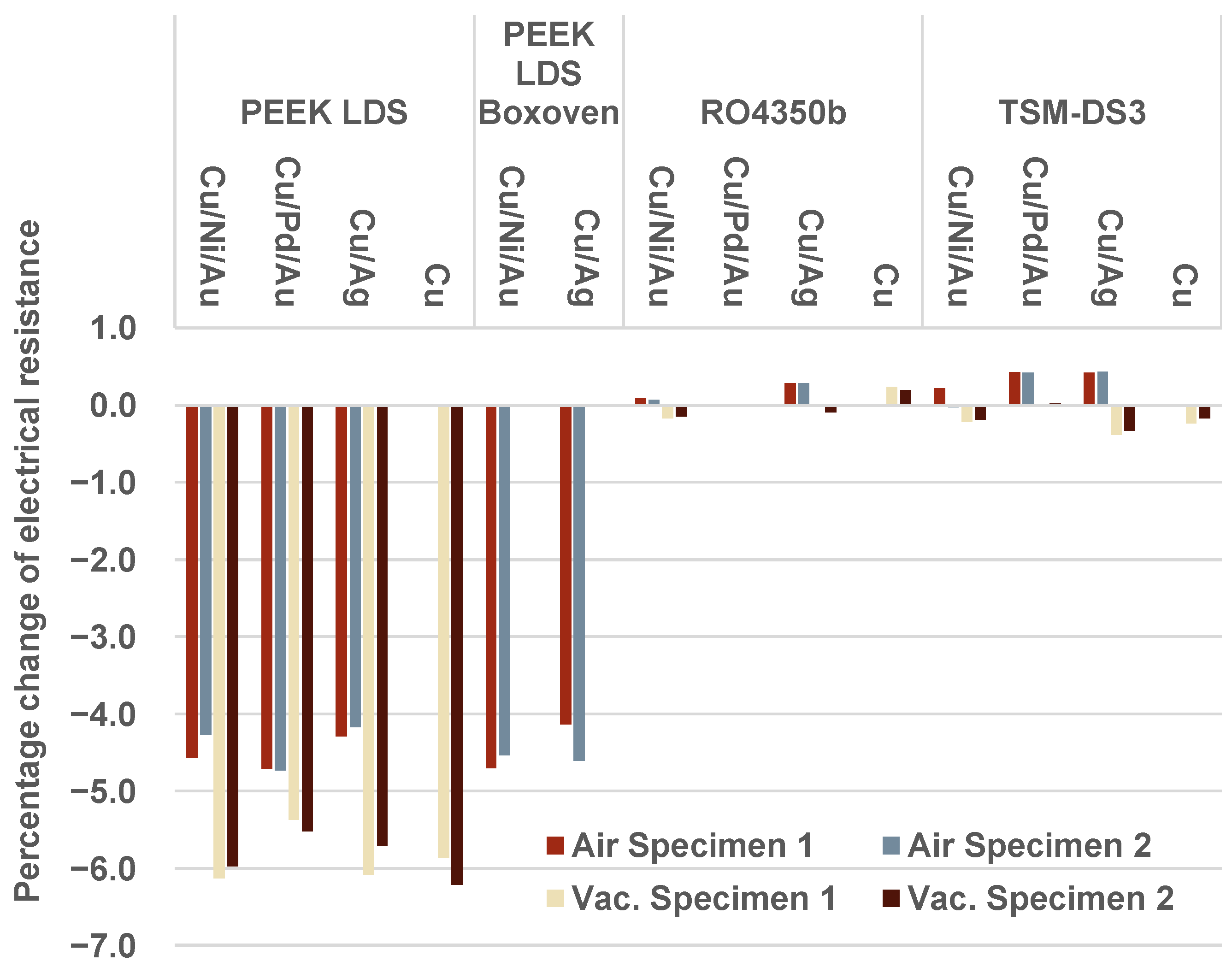
In Figure 10, the results on changes of the electrical resistances of the meander are depicted. For RO4350b and TSM-DS 3 substrates no significant changes in electrical resistance can be observed. This is to be expected for electrodeposited or rolled copper foils, which are usually used in PCB laminates. For PEEK LDS the electrical resistance of the meander decreases after tempering in a vacuum slightly more than after tempering in air. Additionally, as expected, box oven tempering resulted in similar decreases as tempering in air.

3.6. Experiment 3: Effects of Different Tempering Times and Temperatures

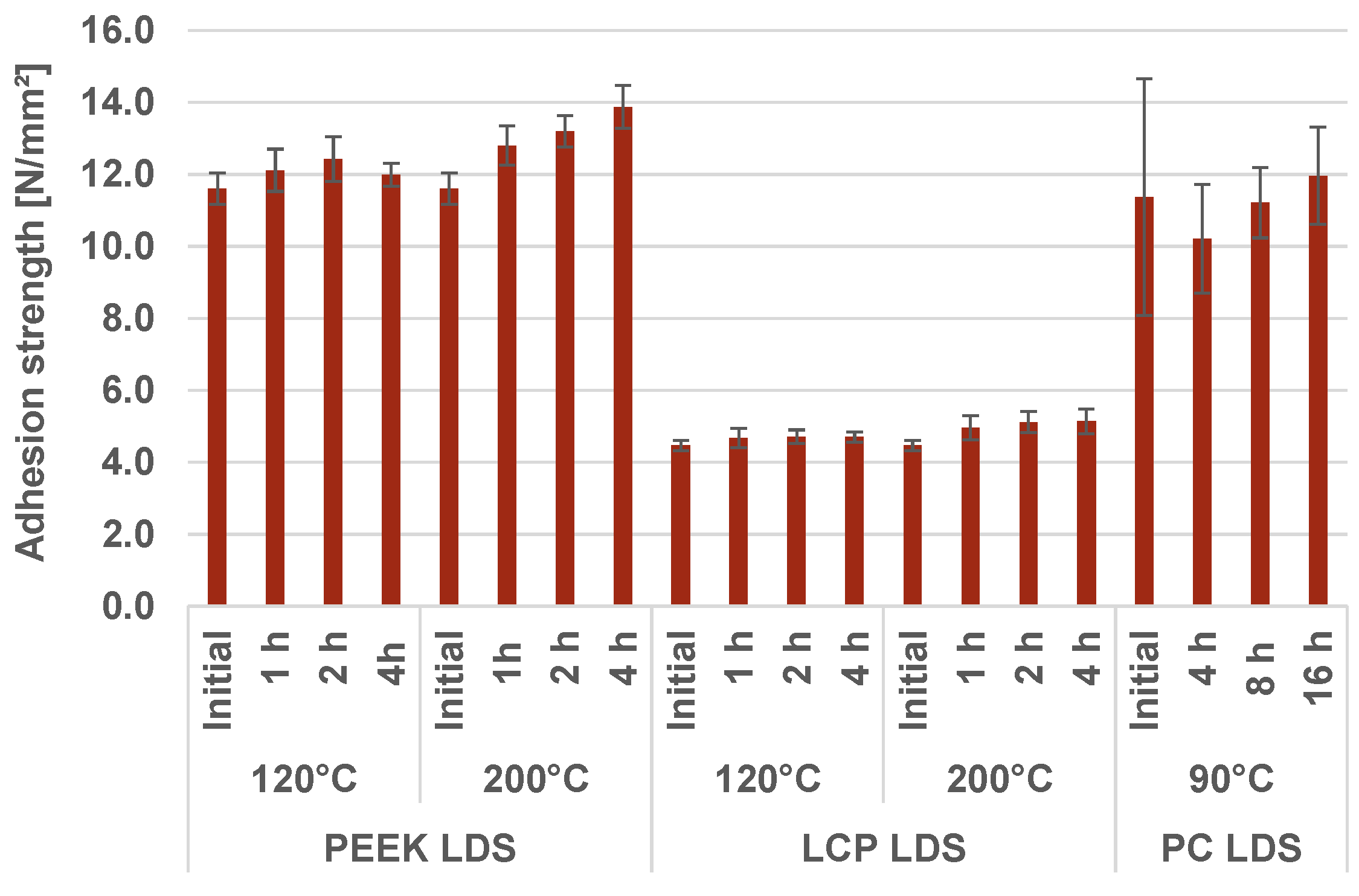
The results on different substrate materials with copper metallization and Pd/Au finish show a direct correlation between adhesion strength and tempering temperature. From Figure 11 it is recognizable that tempering of LCP LDS and PEEK LDS substrates at 200 °C causes a stronger increase in adhesion strength compared to tempering at 120 °C. Additionally, tempering LCP LDS at both temperatures and PEEK LDS at 120 °C for longer than one hour seems to not further improve the adhesion strength. Tempering PEEK LDS substrates at 200 °C for longer times on the other hand seems not to exhibit the same behavior, but a constant increase in adhesion over time. For PC LDS substrates no significant effect was observed, similar to experiment 1, but the standard deviation of the adhesion strength measurements decreased.
As shown in Figure 12, the changes of electrical resistances of the meander depends on the tempering temperature. No clear influence of the tempering time can be observed for PEEK LDS and LCP LDS substrates. For LCP LDS substrates tempered for two and four hours, one of two specimens failed due to delamination or micro cracks of the metallization, which is probably due to the low adhesion strength and inherent compressive stress of the electroless copper metallization (red cross in Figure 12). PC LDS exhibits a lower decrease in electrical resistances of the meander, like in experiment one, but with a continuous increase with prolonged tempering process. In Figure 13, dielectric measurements at 500 MHz are shown. Similar to the results shown in Figure 8 no changes due to the tempering processes are visible.

4. Discussion

The results show that tempering processes can be beneficial for the adhesion strength and electrical resistance of the metallization on LDS-MID based on high temperature thermoplastics like LCP and PEEK.
The reduction in the electrical resistance of the metallization was independent from heating rate, substrate material, and applied surface finish. However, the application of vacuum during the tempering step significantly reduced of the electrical resistance. In experiment 2, an overall reduction in the electrical resistance after tempering in air of approximately 4% was observed whereas the influence of vacuum further decreased it to 6%. Furthermore, the tempering temperature showed a significant impact in experiment 3 for PEEK LDS and LCP LDS substrates. Tempering at 200 °C reduced the electrical resistance up to 5%, while tempering at 120 °C reduced the electrical resistance significantly less. Additionally, a reduction in tempering time to 1 h or an extension up to 4 h showed no significant impact, implying that the modifications within the electroless deposited copper layer were already completed after 1 h. For PC LDS on the other hand only small changes in the electrical resistance were observed due to the relatively low tempering temperature of about 90 °C. Like for the other two LDS-MID substrates the heating rate showed no significant impact, but the extension of the tempering time from 4 h to 8 and 16 h caused a further decrease in the electrical resistance. Similar results were presented in [33]. They reported on a resistivity of an electroless deposited copper film of about 4.6 μ /cm that decreased after tempering at 400 °C in an N2/H2 atmosphere down to 1.75 μ /cm, while [34] reported on a drop of electrical resistivity from 6.23 μ /cm as deposited down to 2.9 μ /cm after 60 min tempering at 300 °C. An extended tempering time did not increase the conductivity any further. These relatively large changes, compared to the results in this publication can be explained by the comparatively thin copper layers in these publications.
While the increase in heating rate induced a further increase in adhesion strength for PEEK LDS substrates, no such behavior was observed for LCP LDS substrates. In experiment 2 the influence of tempering in a vacuum on the adhesion strength was measured. As stated by Eisch et al. and Porta et al., a possible explanation for the increase in adhesion strength could be the oxidation of copper at the interface between polymer and metallization [21,25]. This theory is backed by Chen et al. who report on a shear strength increase from 54 g/mm² up to 183 g/mm² of electroless copper on LCP after an tempering at 150 °C [20]. On the other hand such an increase in adhesion strength is not only limited to electroless copper on polymers, but also for other substrates. This is in accordance with reported tempering of electroless copper films on silicon wafers, whereas the adhesion strength improved with increasing temperature [24]. From experiment 3, a clear influence of tempering time on the adhesion strength can be observed. While for PEEK LDS and LCP LDS substrates the tempering effect at 120 °C on adhesion strength seem to level of after two hours, the same statement cannot be made for the tempering temperature of 200 °C. Here only for LCP LDS substrates a leveling out at one hour was observed, while for PEEK LDS substrates a continuous increase in adhesion strength can be observed even up to a four hour tempering step. A possible explanation could be derived from the different oxygen permeability of LCP and PEEK. LCP has a much lower oxygen permeability than PEEK. The material data sheet states an oxygen permeability for LCP of 0.0225 cm 3 · mm / m 2 · day · bar (unit modified) [35], while values of 506–1370 cm 3 · mm / m 2 · day · bar (unit modified) for different PEEK substrates were reported [36]. During tempering oxygen permeates the polymer and thus causing the formation of copper oxide at the interface to the polymer substrate. The progress of the reaction is limited by the oxygen permeation through the polymer. The very low oxygen permeability of LCP could then result in oxygen depletion and limit copper oxidation at the interface.
For PC LDS substrates tempering reduced the very high standard deviation of the adhesion strength caused by the relatively low temperature stability of the material. This is probably linked to the reduction in internal stress in the injection molded polymer substrate. For comparison, the applied tempering processes had no significant influence on the copper metallization of both investigated HF PCB substrates.

5. Conclusions

The beneficial effect of tempering electroless copper on different substrates is known from the literature for some time. In this paper, tempering LDS-MID and HF PCB substrates is presented and the effects of different process parameters on the substrates properties. The following points can be summarized and highlighted from this study:
  • Tempering of high temperature capable LDS-MID substrates can increase the adhesion strength of the metallization and lower the electrical resistance significantly.
  • Tempering in air seems to be more beneficial as it increases the adhesion strength of the metallization much more than tempering in a vacuum as seen in experiment two. As delamination is high risk in many applications, the reliability of given devices will benefit therefor more from tempering in air.
  • Tempering in a vacuum seemed to decrease the electrical resistance of the metallization on PEEK LDS substrates slightly stronger compared to tempering in air.
  • The decrease in electrical resistance is mainly influenced by the tempering temperature and an increase in tempering time from one to four hours did not further decrease the electrical resistance.
  • Tempering of PC LDS substrates reduced the electrical resistance of the metallization only marginally as the used temperature is to low to induce major changes in the metallization
  • Tempering of PC LDS substrates did not improve the adhesion strength of the metallization but lowered the standard deviation. In experiment three the standard deviation of the measurements decreased from 3.3 μ m to values between 1.0 μ m to 1.5 μ m.
  • Tempering of the HF PCB substrates did not affect the electrical resistance or adhesion strength of the metallization.
  • The dielectrical properties of the LDS-MID materials were not influenced by the tempering processes.
From those conclusions, it can be deduced that tempering 3D circuit carriers manufactured by LDS technology could enhance their performance and reliability. This should be further investigated by accelerated aging tests like temperature shock tests or damp heat storage tests of untempered and tempered LDS-MID.

Author Contributions

Conceptualization, M.W.; methodology, M.W. and L.S.; formal analysis, M.W. and L.S.; investigation, M.W. and L.S.; data curation, M.W. and L.S.; writing—original draft preparation, M.W. and K.W.; writing—review and editing, T.G. and W.E.; visualization, M.W. and L.S.; supervision, T.G. and W.E.; funding acquisition, T.G. and A.Z.; project administration, A.Z. All authors have read and agreed to the published version of the manuscript.

Funding

This publication was funded via AiF, grant number 20668 N, within the programme for promoting the Industrial Collective Research (IGF) of the Federal Ministry of Economic Affairs and Climate Action (BMWK), based on a resolution of the German Parliament. This publication was funded by the German Research Foundation (DFG) grant “Open Access Publication Funding/2023–2024/University of Stuttgart” (512689491).

Data Availability Statement

All data used are shown in the text. Raw data are available on request.

Acknowledgments

The authors would like to acknowledge the support of the BMWK.

Conflicts of Interest

The authors declare no conflict of interest.

Abbreviations

The following abbreviations are used in this manuscript:
LCPLiquid crystal polymer
PEEKPoly-ether-ether-ketone
PCPolycarbonate
PTFEPolytetrafluoroethylene
DkPermittivity
DfDielectric loss factor
HFHigh frequency
LDSLaser direct structuring
MIDMechatronic integrated devices
5GFifth-generation technology standard for broadband cellular networks
PCBPrinted circuit boards
3DThree dimensional

References

  1. Liu, D.; Pfeiffer, U.; Grzyb, J.; Gaucher, B. Advanced Millimeter-Wave Technologies: Antennas, Packaging and Circuits; John Wiley & Sons: Hoboken, NJ, USA, 2009. [Google Scholar]
  2. Elisabeth, S. Advanced RF packaging technology trends, from WLP and 3D integration to 5G and mmWave applications. In Proceedings of the 2019 International Wafer Level Packaging Conference (IWLPC), San Jose, CA, USA, 22–24 October 2019; pp. 1–5. [Google Scholar]
  3. 3dFortify Inc. Millimeter-Wave Hits the Mainstream, along with All the Challenges of High Frequency Design & Fabrication. Available online: https://www.microwavejournal.com/articles/36990-millimeter-wave-hits-the-mainstream-along-with-all-the-challenges-of-high-frequency-design-and-fabrication?page=2 (accessed on 6 March 2023).
  4. Franke, J. Three-Dimensional Molded Interconnect Devices (3D-MID); Carl Hanser Verlag: Munich, Germany, 2014. [Google Scholar]
  5. Eberhardt, W.; Weser, S. Cleaning Processes for Laser Based Fine Pitch Molded Interconnect Devices. In Proceedings of the 10th International Congress MID 2012, Nuremberg-Fuerth, Germany, 19–20 September 2012. [Google Scholar]
  6. Kildal, S.S.; Pfuhl, N.; Flamini, R.; Biscontini, B. Molded interconnect device (MID) design for base station antenna elements. In Proceedings of the 2016 IEEE International Symposium on Antennas and Propagation (APSURSI), Fajardo, PR, USA, 26 June–1 July 2016; pp. 1845–1846. [Google Scholar]
  7. Chen, Y.; Zhang, C.; Lu, Y.; Yang, W.W.; Huang, J. Compact dual-polarized base station antenna array using laser direct structuring technique. IEEE Antennas Wirel. Propag. Lett. 2020, 20, 78–82. [Google Scholar] [CrossRef]
  8. Molex-LLC. RHCP LDS SMT GPS Antenna. Available online: https://www.molex.com/molex/products/family/gnssgps{_}antennas (accessed on 6 March 2023).
  9. Glise, A.; Quéré, Y.; Maalouf, A.; Rius, E.; Castel, V.; Laur, V.; Sauvage, R. LDS Realization of High-Q SIW Millimeter Wave Filters with Cyclo-Olefin Polymers. Appl. Sci. 2018, 8, 2230. [Google Scholar] [CrossRef] [Green Version]
  10. Laur, V.; Mattei, J.L.; Vérissimo, G.; Queffelec, P.; Lebourgeois, R.; Ganne, J.P. Application of Molded Interconnect Device technology to the realization of a self-biased circulator. J. Magn. Magn. Mater. 2016, 404, 126–132. [Google Scholar] [CrossRef]
  11. Friedrich, A.; Geck, B.; Fengler, M.; Fischer, A. 24 GHz dielectric filled waveguide fed horn antenna using 3D-LDS MID technology. In Proceedings of the Microwave Conference (EuMC), 2016 46th European, London, UK, 4–6 October 2016; pp. 739–742. [Google Scholar]
  12. Friedrich, A.; Geck, B.; Fengler, M. LDS manufacturing technology for next generation radio frequency applications. In Proceedings of the 2016 12th International Congress Molded Interconnect Devices (MID), Wuerzburg, Germany, 28–29 September 2016; pp. 1–6. [Google Scholar] [CrossRef]
  13. Friedrich, A.; Fengler, M.; Geck, B.; Manteuffel, D. 60 GHz 3D integrated waveguide fed antennas using laser direct structuring technology. In Proceedings of the 2017 11th European Conference on Antennas and Propagation (EUCAP), Paris, France, 19–24 March 2017; pp. 2507–2510. [Google Scholar] [CrossRef]
  14. Seewald, S.; Manteuffel, D. Integration of a 28 GHz Beamforming Module into a Handset Device Using LDS-MID Technology. In Proceedings of the 2021 IEEE International Symposium on Antennas and Propagation and USNC-URSI Radio Science Meeting, Singapore, 4–10 December 2021. [Google Scholar]
  15. Seewald, S.; Manteuffel, D.; Wolf, M.; Barth, M.; Eberhardt, W.; Zimmermann, A. Low-Loss 3D-Coplanar Line Structure for Millimeter Wave Applications Using Laser Direct Structuring Technology. In Proceedings of the 2021 International Conference on Electromagnetics in Advanced Applications (ICEAA), Honolulu, HI, USA, 9–13 August 2021; p. 85. [Google Scholar]
  16. Nakahara, S.; Mak, C.; Okinaka, Y. Effect of Low-Temperature (100–200 °C) Annealing on the Ductility of Electroless Copper. J. Electrochem. Soc. 1991, 138, 1421. [Google Scholar] [CrossRef]
  17. Wheeler, H. Formulas for the Skin Effect. Proc. IRE 1942, 30, 412–424. [Google Scholar] [CrossRef]
  18. Mak, C.; Nakahara, S.; Okinaka, Y.; Trop, H.; Taylor, J. Annealing Behavior of Fine-Grained Electroless Copper Deposits. J. Electrochem. Soc. 1993, 140, 2363. [Google Scholar] [CrossRef]
  19. Koo, H.C.; Lightsey, C.; Kohl, P.A. Affect of Anneal Temperature on All-Copper Flip-Chip Connections Formed via Electroless Copper Deposition. IEEE Trans. Compon. Packag. Manuf. Technol. 2011, 2, 79–84. [Google Scholar] [CrossRef]
  20. Chen, L.; Crnic, M.; Lai, Z.; Liu, J. Process development and adhesion behavior of electroless copper on liquid crystal polymer (LCP) for electronic packaging application. IEEE Trans. Electron. Packag. Manuf. 2002, 25, 273–278. [Google Scholar] [CrossRef]
  21. Eisch, J.; Laskowski, J.; Bielinski, J.; Bolesławski, M. The deposition and adhesion of copper films on smooth polymer surfaces. J. Mater. Sci. Lett. 1995, 14, 146–147. [Google Scholar] [CrossRef]
  22. Okinaka, Y.; Nakahara, S. Hydrogen embrittlement of electroless copper deposits. J. Electrochem. Soc. 1976, 123, 475. [Google Scholar] [CrossRef]
  23. Okinaka, Y.; Straschil, H. The effect of inclusions on the ductility of electroless copper deposits. J. Electrochem. Soc. 1986, 133, 2608. [Google Scholar] [CrossRef]
  24. Lin, J.H.; Lee, T.L.; Hsieh, W.J.; Lin, C.C.; Kou, C.S.; Shih, H.C. Interfacial mechanism studies of electroless plated Cu films on a-Ta: N layers catalyzed by PIII. J. Vac. Sci. Technol. A Vac. Surfaces Film. 2002, 20, 733–740. [Google Scholar] [CrossRef] [Green Version]
  25. Porta, G.M.; Foust, D.F.; Burrell, M.C.; Karas, B.R. Vacuum metallization of polyetherimide: Interfacial chemistry and adhesion. Polym. Eng. Sci. 1992, 32, 1021–1027. [Google Scholar] [CrossRef]
  26. Lee, C.H.; Kim, J.J. Self-annealing effect of electrolessly deposited copper thin films based on Co (ii)–ethylenediamine as a reducing agent. J. Vac. Sci. Technol. B Microelectron. Nanometer Struct. Process. Meas. Phenom. 2004, 22, 180–184. [Google Scholar] [CrossRef]
  27. Mitsubishi Engineering Plastics Corp. XANTAR LDS 3760® LDS 3760; Mitsubishi Engineering Plastics Corp: Tokyo, Japan, 2017. [Google Scholar]
  28. Ensinger GmbH. TECACOMP® LCP LDS Black 4107; Ensinger GmbH: Nufringen, Germany, 2016. [Google Scholar]
  29. Ensinger GmbH. TECACOMP® PEEK LDS Black 1047045; Ensinger GmbH: Nufringen, Germany, 2019. [Google Scholar]
  30. Rogers Corp. RO4000 Series High Frequency Circuit Materials Data Sheet; Rogers Corp: Chandler, AZ, USA, 2022. [Google Scholar]
  31. AGC Inc. TSM-DS3 Dimensionally Stable Low Loss Laminate; AGC Inc.: Tokyo, Japan, 2022. [Google Scholar]
  32. Kuhn, T. Qualität und Zuverlässigkeit Laserdirektstrukturierter Mechatronisch Integrierter Baugruppen (LDS-MID); FAU University Press: Erlangen, Germany, 2020. [Google Scholar]
  33. Hsu, H.H.; Lin, K.H.; Lin, S.J.; Yeh, J.W. Electroless copper deposition for ultralarge-scale integration. J. Electrochem. Soc. 2001, 148, C47. [Google Scholar] [CrossRef]
  34. Aithal, R.K.; Yenamandra, S.; Gunasekaran, R.; Coane, P.; Varahramyan, K. Electroless copper deposition on silicon with titanium seed layer. Mater. Chem. Phys. 2006, 98, 95–102. [Google Scholar] [CrossRef]
  35. Celanese Corp. Vectra® LCP Design Guide; Celanese Corp: Dallas, TX, USA, 2013. [Google Scholar]
  36. Monson, L.; Moon, S.I.; Extrand, C. Permeation resistance of poly (ether ether ketone) to hydrogen, nitrogen, and oxygen gases. J. Appl. Polym. Sci. 2013, 127, 1637–1642. [Google Scholar] [CrossRef]
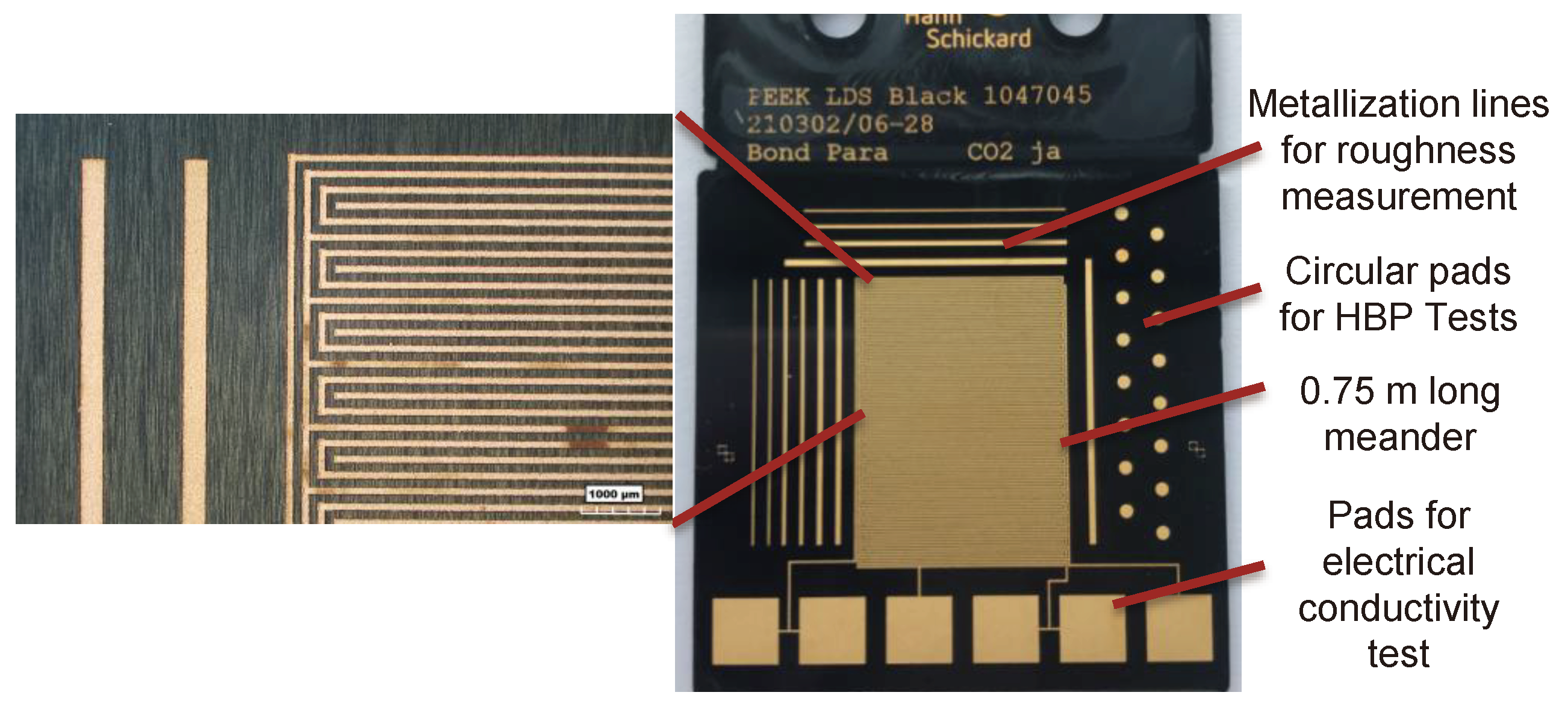
Figure 1. Typical metallization layout of the specimens.
Jmmp 07 00139 g001
Figure 2. The subfigure labels are (a) Metallization on RO4350b, (b) standard metallization on LCP LDS, and (c) optimized metallization on LCP LDS.
Jmmp 07 00139 g002
Figure 3. Schematics of a hot-bump-pull test [32].
Jmmp 07 00139 g003
Figure 4. Initial characterization of adhesion strength.
Jmmp 07 00139 g004
Figure 5. Initial characterization of electrical resistance of meander.
Jmmp 07 00139 g005
Figure 6. Adhesion strength depending on heating rates.
Jmmp 07 00139 g006
Figure 7. Percentual electrical resistance changes of the meander depending on heating rate.
Jmmp 07 00139 g007
Figure 8. Dielectrical properties of LDS-MID substrates at 500 MHz after experiment 1.
Jmmp 07 00139 g008
Figure 9. Adhesion strength depending on applied surface finish and tempering atmosphere.
Jmmp 07 00139 g009
Figure 10. Percentual electrical resistance changes of the meander depending on applied surface finishes and tempering conditions.
Jmmp 07 00139 g010
Figure 11. Adhesion strength depending on of tempering times and temperatures.
Jmmp 07 00139 g011
Figure 12. Percentual electrical resistance changes of the meander depending on tempering times and temperatures.
Jmmp 07 00139 g012
Figure 13. Dielectric properties of LDS-MID substrates at 500 MHz after experiment 3.
Jmmp 07 00139 g013
Table 1. Substrate materials.
Substrate MaterialAcronymTechnologyMatrix
Material
Heat Distortion
Temperature
(°C)
Melting
Temperature
(°C)
Rogers
Ro4350b
Ro4350bHF-PCBThermoset>280-
Taconic
TSM-DS 3
TSM-DS 3HF-PCBPTFE-321–344
Xantar
3760 LDS
PC LDSLDS-MIDPC103-
Tecacomp LCP
LDS black 4107
LCP LDSLDS-MIDLCP274320
Tecacomp PEEK
LDS black 1047045
PEEK LDSLDS-MIDPEEK255343
Table 2. Temperature profile for hot-bump-pull test.
Substrate
Material
Pre-Heating PhasePeak PhaseStart of Pull Force
Temp.
(°C)
Dwell
Time (s)
Temp.
(°C)
Dwell
Time (s)
Temp.
(°C)
RO4350b
TSM-DS3
PC LDS
LCP LDS
1402160650
PEEK LDS1408180850
Table 3. Geometrical dimensions of copper metallization without finish, measured by optical microscopy.
Ro4350bTSM-DS3PEEK LDSLCP LDSPC LDS
Transmission line width(µm)104104656983
Transmission line height(µm)1715111311
Cross section area(µm²)17681560715897913
Table 4. Comparison of dielectric properties.
RO4350b
(@10 GHz)
TSM-DS3
(@10 GHz)
PC LDS
(@1 GHz)
LCP LDS
(@1 GHz)
PEEK LDS
(@1 GHz)
Dk3.483.02.93.33.4
Df0.00370.00140.0060.0050.0025
Disclaimer/Publisher’s Note: The statements, opinions and data contained in all publications are solely those of the individual author(s) and contributor(s) and not of MDPI and/or the editor(s). MDPI and/or the editor(s) disclaim responsibility for any injury to people or property resulting from any ideas, methods, instructions or products referred to in the content.