
Progress in Thin-Film Photovoltaics: A Review of Key Strategies to Enhance the Efficiency of CIGS, CdTe, and CZTSSe Solar Cells


Abstract
1. Introduction
2. Key Thin-Film Absorber Materials
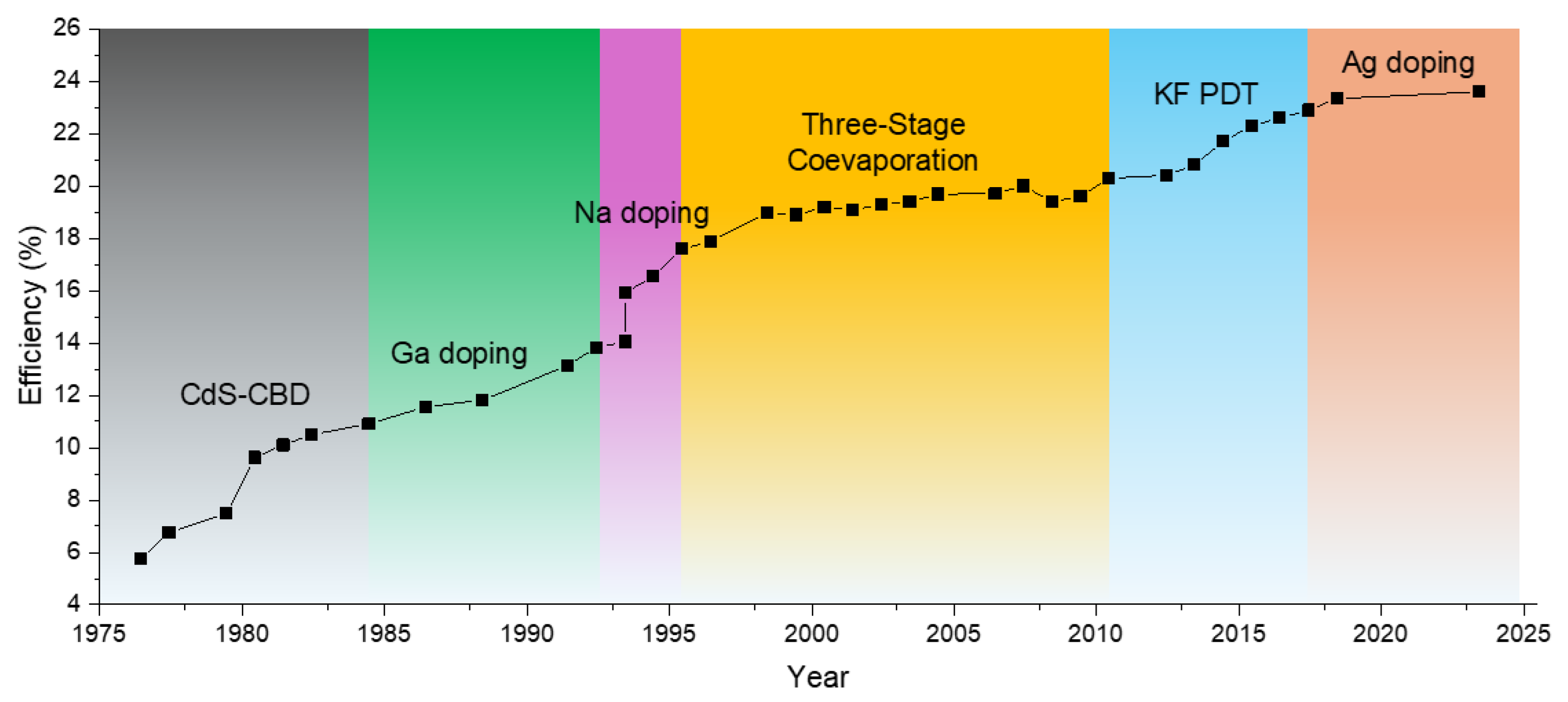
2.1. CIGS

| Year | CIGS Grading Strategy | Voc (V) | Jsc (mA/cm2) | FF (%) | η (%) | Ref. |
|---|---|---|---|---|---|---|
| 1993 | Physical vapour deposition (PVD) | 0.7 | – | – | 12.2 | [26] |
| 1994 | Co-evaporation of In, Ga, and Se | 0.649 | 31.88 | 76.6 | 15.9 | [27] |
| 1996 | PVD | 0.642 | 31.9 | 73.7 | 15.1 | [28] |
| 2001 | Three-stage process | 0.691 | 33 | 76 | 16.7 | [29] |
| 2003 | Co-evaporation | 0.625 | 29.4 | 72 | 14.2 | [30] |
| 2003 | Co-evaporation | 0.66 | 31.9 | 76 | 16.1 | [31] |
| 2003 | Three-stage process | 0.689 | 35.71 | 78.12 | 19.2 | [32] |
| 2008 | Co-evaporation | 0.69 | 35.5 | 81.2 | 19.9 | [33] |
| 2011 | Co-evaporation | 0.74 | 35.4 | 77.5 | 20.3 | [34] |
| 2011 | Three-stage process | 0.665 | 31.1 | 73.6 | 15.5 | [35] |
| 2013 | Co-evaporation | 0.723 | 33.76 | 76.09 | 18.56 | [36] |
| 2015 | Sequential evaporation | 0.674/0.725 | 33.2/34.20 | 74.8/80.50 | 16.7/20.0 | [37] |
| 2016 | Three-stage process | 0.6 | 28 | 74 | 12.1 | [38] |
| 2017 | Co-evaporation | 0.718 | 35.9 | 76.8 | 19.9 | [39] |
| 2019 | Three-stage process | 0.498 | 37 | 74 | 13.6 | [40] |
| 2019 | Three-stage process | 0.61 | 30.53 | 60.71 | 11.7 | [41] |
| 2019 | Co-evaporation | 0.731 | 36.6 | 75.9 | 20.3 | [42] |
| 2019 | Co-evaporation | 0.65 | 28 | 70 | 12 | [43] |
| 2019 | Sequential sputtering with sulfurization after selenization | 0.73 | 41.9 | 79 | 23.35 | [44] |
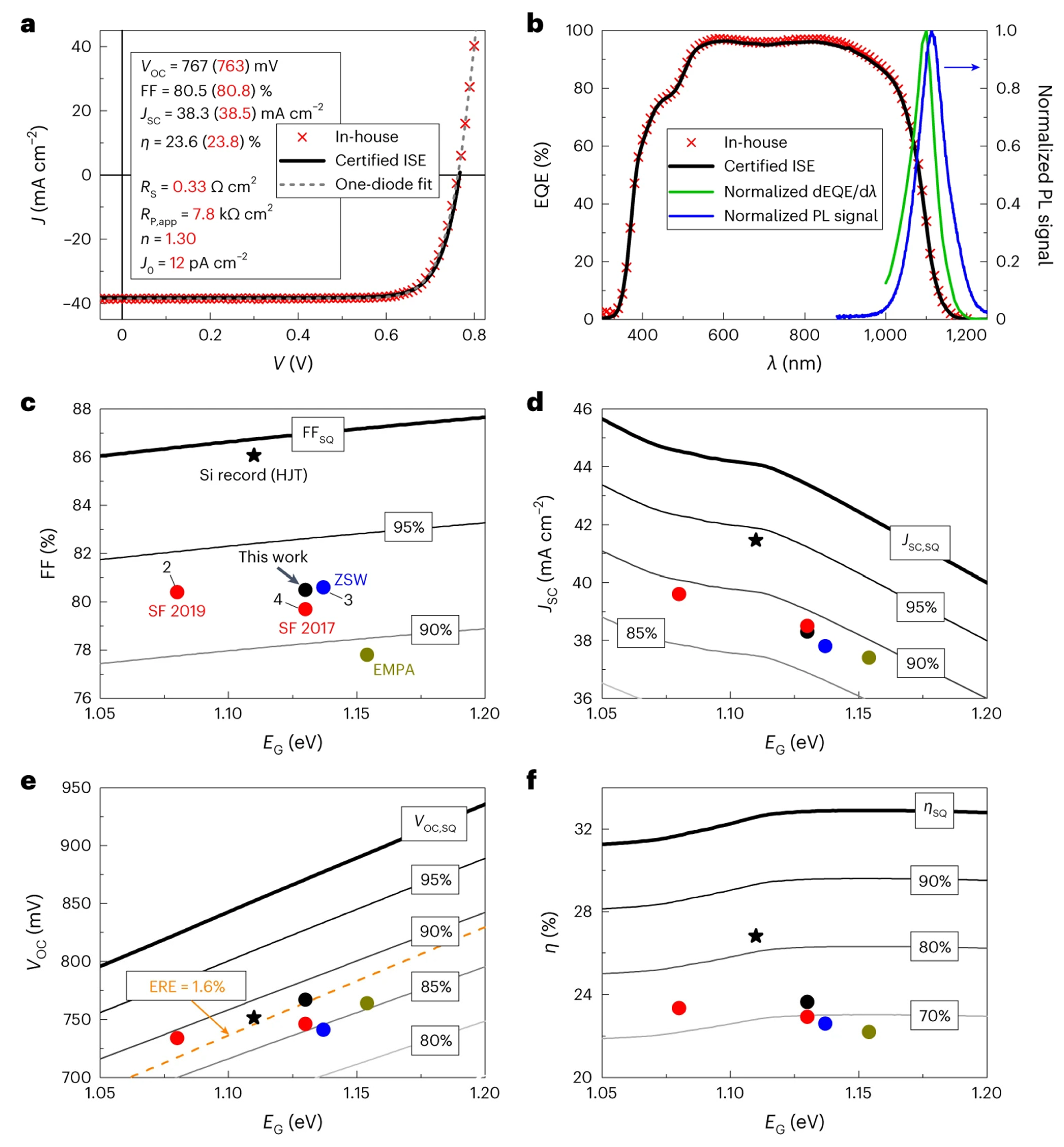
| 2024 | Co-evaporation | 0.767 | 38.3 | 80.5 | 23.6 | [23] |
| Manufacturer | Process | Voc (V) * | Jsc (A) * | FF (%) * | η (%) * | Country | Ref |
|---|---|---|---|---|---|---|---|
| Solar Frontier | Sputtering | 112 | 2.2 | 68.9 | 13.8 | Japan | [45] |
| MiaSolé | Sputtering | 37.8 | 4.58 | 70.7 | 17 | USA | [46] |
| Ascent Solar | Co-evaporation | 23 | 3.55 | 58 | 17.55 | USA | [47] |
| Sunflare | Co-evaporation | 36.6 | 7.5 | 67 | 15 | USA | [48] |
| Eterbright Solar Corp. | Co-evaporation | 74.2 | 2.32 | 69.6 | 14.9 | Taiwan | [49] |
| DS New Energy | Sputtering | 40.92 | 4.52 | 76.1 | 18.3 | China | [50] |
| AVANCIS | Sputtering | 24 | 10.5 | 79.3 | 17.7 | Germany | [51] |
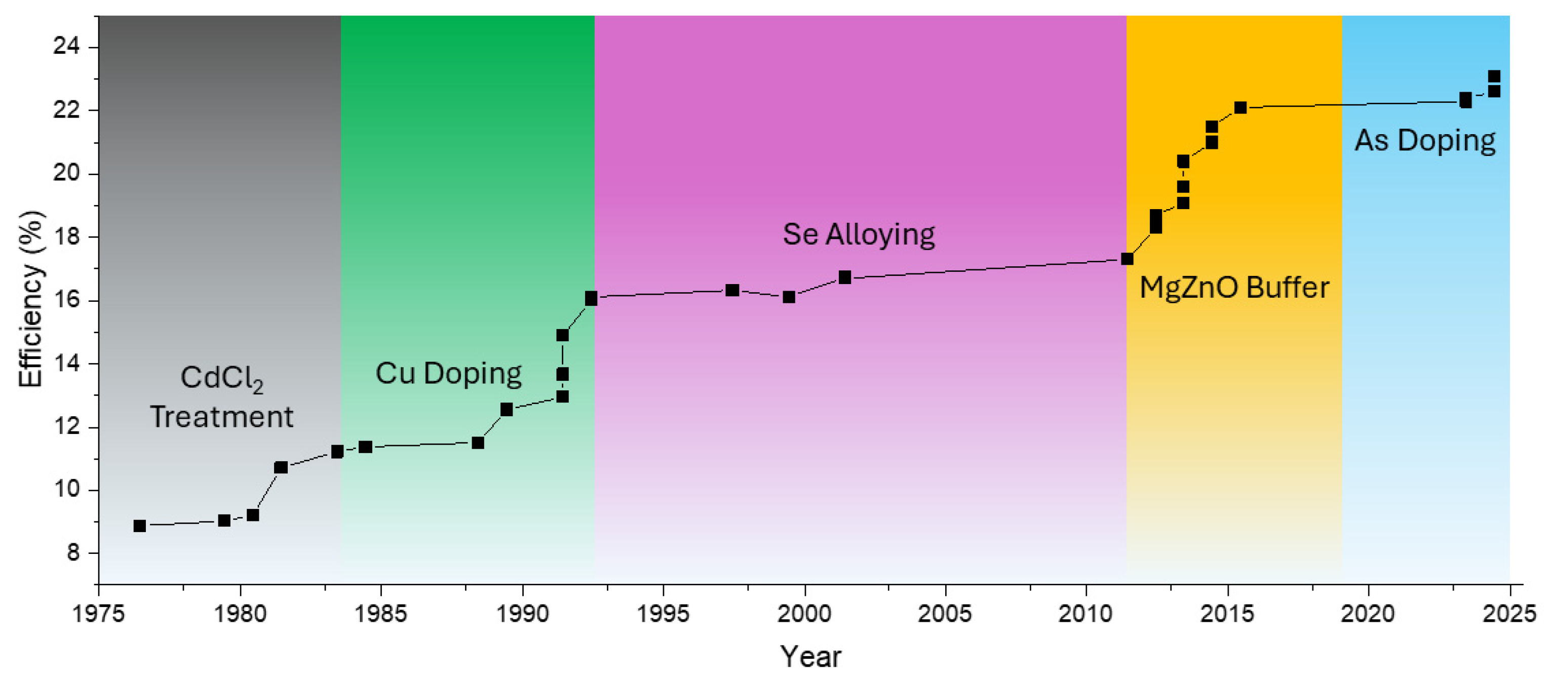
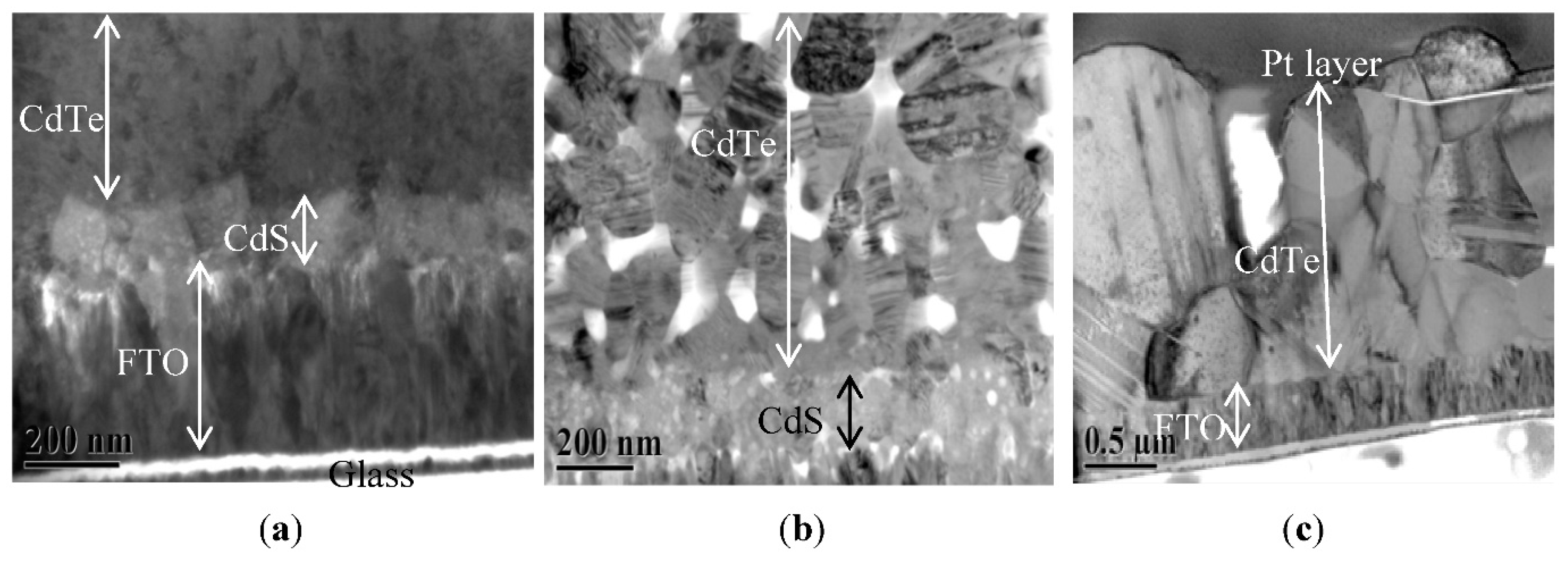
2.2. CdTe
2.3. CZTS/CZTSSe
| Year | CZTS Grading Strategy | Voc (V) | Jsc (mA/cm2) | FF (%) | η (%) | Ref. |
|---|---|---|---|---|---|---|
| 2010 | Hot injection | 0.43 | 31.2 | 53.9 | 7.23 | [81] |
| 2010 | Spin coating (hydrazine solution-based precursor) | 0.516 | 28.6 | 65 | 9.66 | [82] |
| 2010 | Thermal evaporation | 0.499 | 29.55 | 64.3 | 9.5 | [83] |
| 2011 | Spin coating (hydrazine solution-based precursor) | 0.517 | 30.8 | 63.7 | 10.1 | [84] |
| 2012 | Spin coating (hydrazine solution-based precursor) | 0.459 | 34.5 | 69.8 | 11.1 | [85] |
| 2013 | Solution process | 0.505 | 24.5 | 57.83 | 7.17 | [86] |
| 2014 | Spin coating (hydrazine solution-based precursor) | 0.513 | 35.2 | 69.8 | 12.6 | [87] |
| 2014 | Spin coating | 0.52 | 23.28 | 49.6 | 6 | [88] |
| 2014 | Annealing of metal precursor | 0.516 | 34.1 | 62.5 | 11 | [89] |
| 2016 | Sequential sputtering | 0.521 | 34.98 | 67.2 | 12.3 | [90] |
| 2016 | Compound sputtering | 0.61 | 17.5 | – | 6 | [91] |
| 2016 | Doctor-blade pasting | 0.621 | 16.3 | 50.7 | 5.1 | [92] |
| 2017 | Two-step process | 0.444 | 30.9 | 47.5 | 6.4 | [93] |
| 2017 | Two-step process | 0.39 | 33.1 | 59 | 7.5 | [94] |
| 2017 | Doctor-blade pasting | 0.617 | 13.2 | 49.9 | 6 | [95] |
| 2017 | Two-step process | 0.615 | 16.3 | 50.7 | 5.1 | [96] |
| 2017 | Electron beam evaporation | 0.744 | 16 | 46 | 5.5 | [97] |
| 2018 | Two-step sputtering | 0.588 | 22.15 | 46.9 | 6.11 | [98] |
| 2018 | Thermal evaporation | 0.655 | 18.7 | 57.6 | 7 | [99] |
| 2019 | Two-step process | 0.621 | 16.3 | 50.7 | 5.1 | [100] |
| 2019 | Solution process | 0.417 | 36.7 | 52.27 | 8.01 | [101] |
| 2020 | Two-step process | 0.617 | 18 | 54.1 | 6 | [102] |
| 2021 | Two-step process | 0.69 | 17.12 | 37.15 | 4.4 | [103] |
2.4. Economic and Environmental Impacts of TFSCs
2.4.1. Comparison of Production Costs and Economic Returns
2.4.2. Environmental Impact and Sustainability
2.4.3. Large-Scale Applications and Commercial Deployment
3. Strategies to Improve TFSC PCE
3.1. CIGS
3.1.1. Bandgap Engineering
Tailoring Bandgaps for Better Spectral Utilization
Approaching the Shockley–Queisser Limit

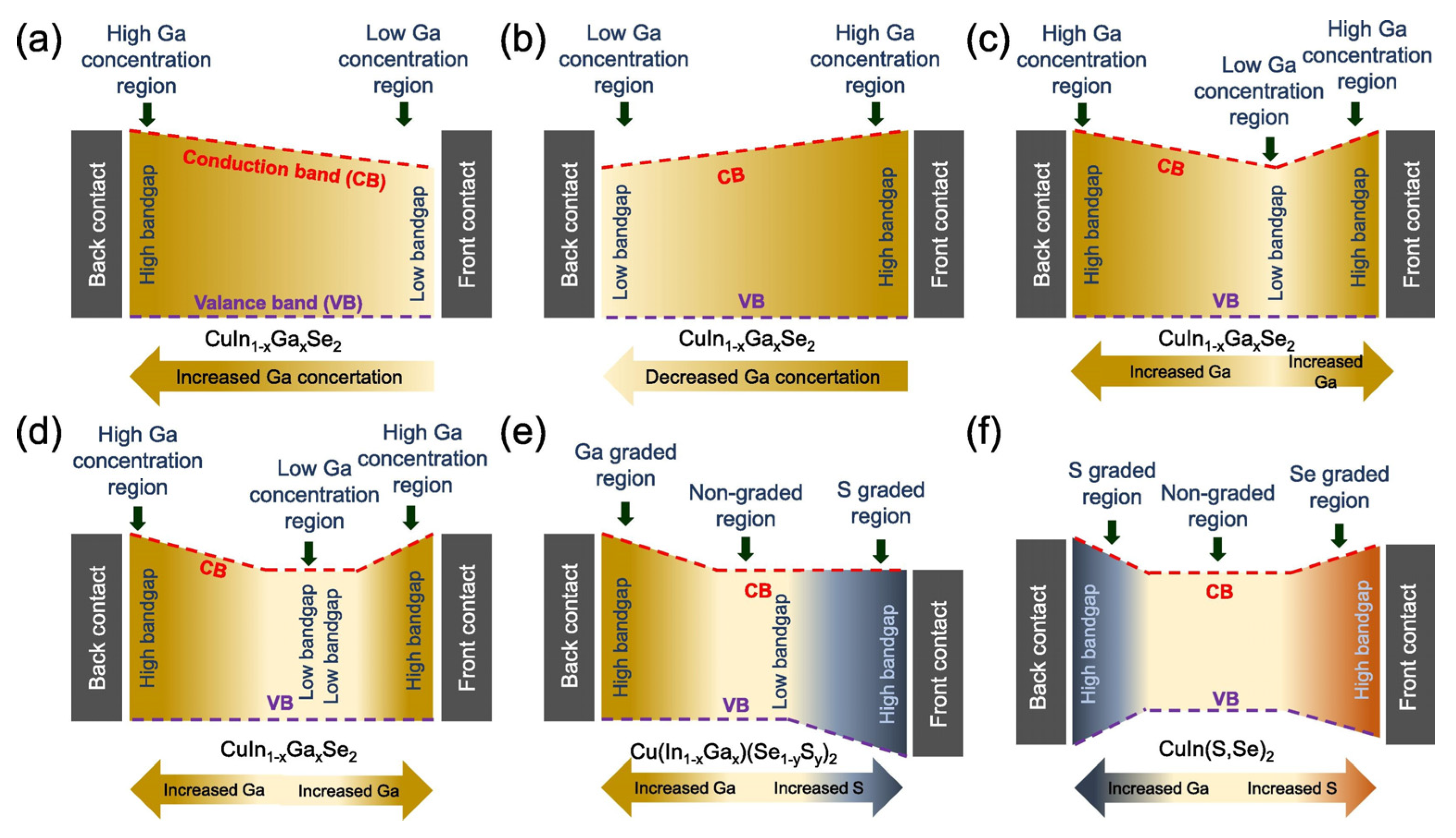
Ga Grading and Its Effect on Bandgap Profile
Al Alloying
3.1.2. Alkali Doping
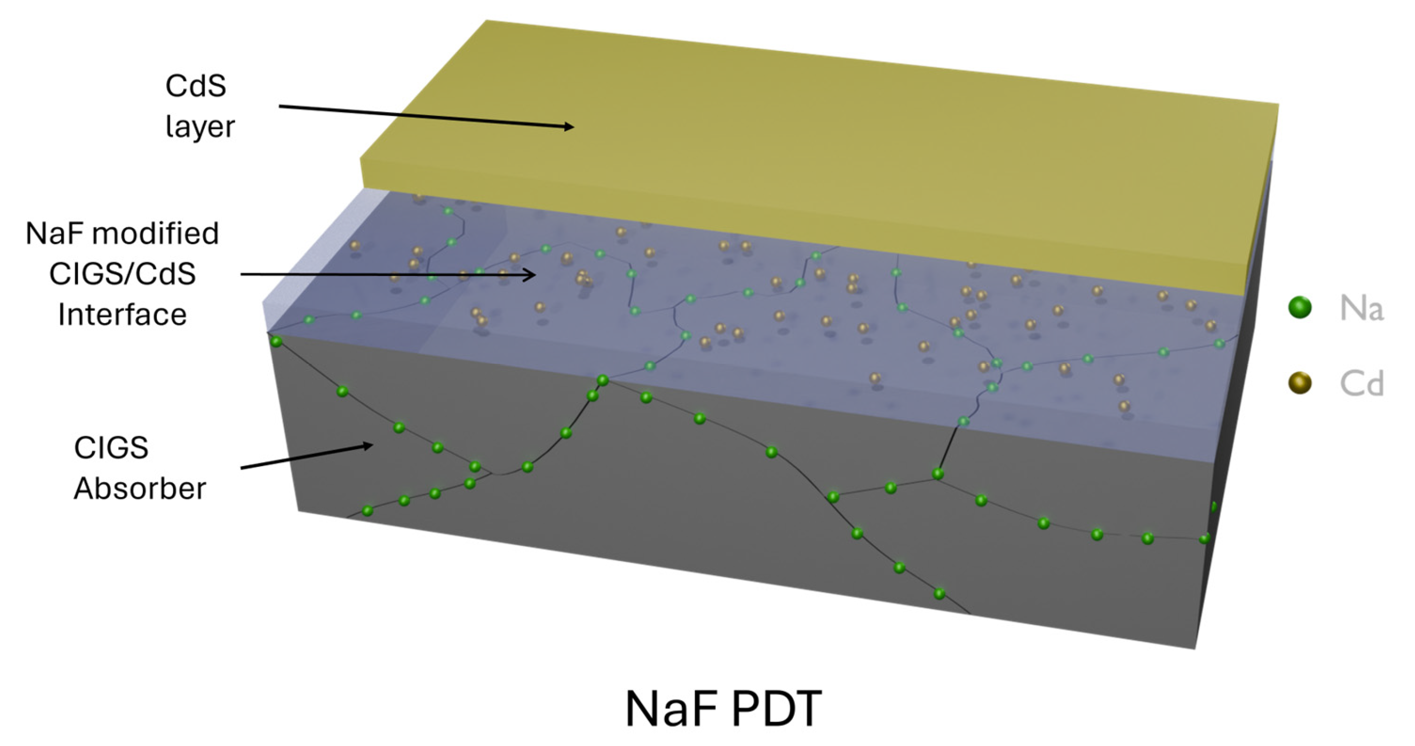
Na as a Foundational Dopant
Potassium (K) as a Complementary Dopant
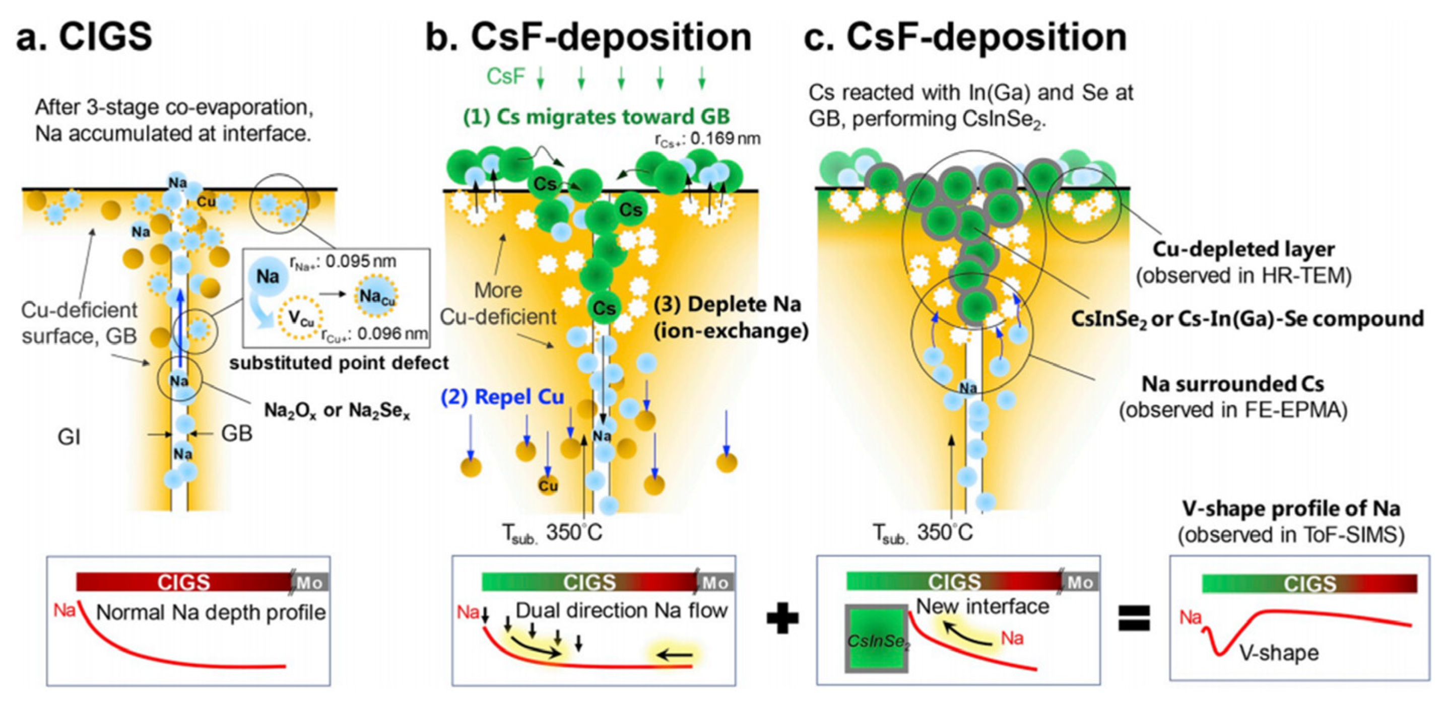
Cs Doping
Rb Doping
3.1.3. Ag Alloying in CIGS
Bandgap Tuning Through Ag Incorporation
Enhancement in Solar Cell Voc and FF
Impact of Ag on Crystallinity, Defect Reduction, and Grain Growth
Trade-Offs in Lattice Mismatch and Defect Formation
3.1.4. Computational Models Predicting Optimal Doping Profiles
3.2. CdTe
3.2.1. Bandgap Engineering
Using Se for Bandgap Tuning
3.2.2. Doping
Cu Doping: Enhancing P-Type Conductivity with Constraints

Cl Doping: Grain Boundary Passivation and Recombination Reduction
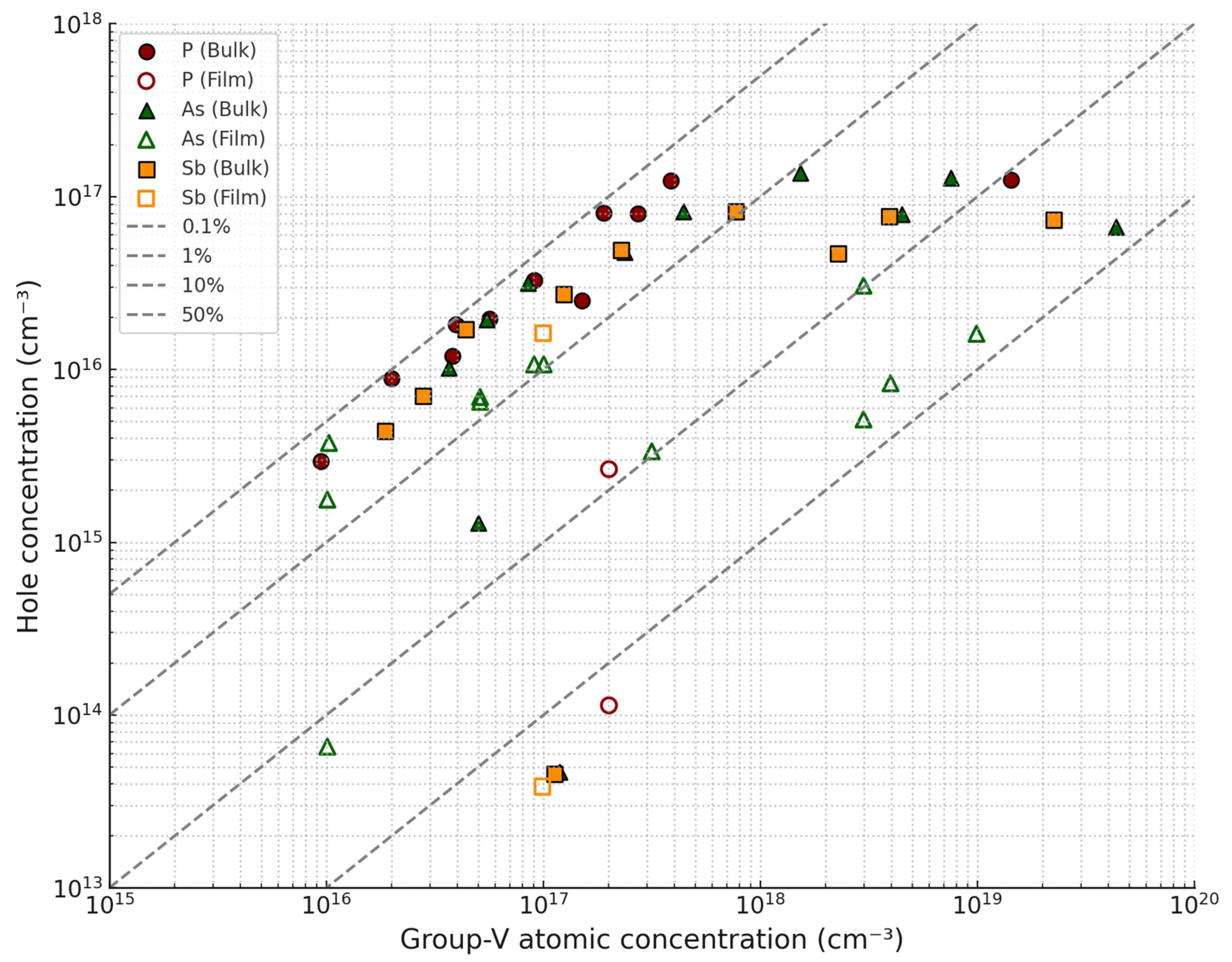
Group V Dopants: Arsenic, Phosphorus, and Sb Doping in CdTe
Interplay of Multiple Dopants in Advanced CdTe Devices
3.2.3. Interface and Buffer Layer Optimization
Using Buffer Layers for Junction Optimization
Impact of Passivation and Carrier Transport on Efficiency
3.3. CZTS/CZTSSe
3.3.1. Bandgap Engineering
Sulfurization and S/Se Ratio Optimization
Challenges in Bandgap Engineering for CZTSSe
3.3.2. Doping Strategies
Ag Doping
Ge Doping
Co Doping
Alkali Metal Doping
3.3.3. Buffer Layer Advancements and Interface Engineering
Buffer Layer Innovations
Defect Passivation at the Interface
Interface Layering
4. Conclusions
Funding
Conflicts of Interest
References
- Oni, A.M.; Mohsin, A.S.M.; Rahman, M.M.; Bhuian, M.B.H. A Comprehensive Evaluation of Solar Cell Technologies, Associated Loss Mechanisms, and Efficiency Enhancement Strategies for Photovoltaic Cells. Energy Rep. 2024, 11, 3345–3366. [Google Scholar]
- Namnuan, B.; Chatraphorn, S. Improving the Photovoltaic Performance of CIGS Solar Cells with the Modified 3-Stage Co-Evaporation Process. Mater. Sci. Semicond. Process. 2024, 179, 108485. [Google Scholar]
- Karami, A.; Morawski, M.; Kempa, H.; Scheer, R.; Cojocaru-Miredin, O. Sodium in Cu(In,Ga)Se2 Solar Cells: To Be or Not to Be Beneficial. Solar RRL 2024, 8, 2300544. [Google Scholar]
- Libório, M.S.; Queiroz, J.C.A.d.; Sivasankar, S.M.; Costa, T.H.d.C.; Cunha, A.F.d.; Amorim, C.d.O. A Review of Cu3BiS3 Thin Films: A Sustainable and Cost-Effective Photovoltaic Material. Crystals 2024, 14, 524. [Google Scholar] [CrossRef]
- Amorim, C.O.; Liborio, M.S.; Queiroz, J.C.A.; Melo, B.M.G.; Sivasankar, S.M.; Costa, T.H.C.; Graça, M.P.F.; da Cunha, A.F. Cu3BiS3 Film Synthesis through Rapid Thermal Processing Sulfurization of Electron Beam Evaporated Precursors. Emergent Mater. 2024, 1–13. [Google Scholar] [CrossRef]
- Santana Liborio, M.; Amorim, C.O.; Queiroz, J.C.A.; Sivasankar, S.M.; Costa, T.H.d.C.; da Cunha, A.F. Strategies to Enhance the Efficiency of Cu3BiS3-Based Photovoltaic Devices: Simulation Insights and Buffer Layer Engineering. ACS Appl. Opt. Mater. 2024, 3, 81–90. [Google Scholar] [CrossRef]
- Kawano, Y.; Chantana, J.; Nishimura, T.; Mavlonov, A.; Minemoto, T. [Ga]/([Ga]+[In]) Profile Controlled through Ga Flux for Performance Improvement of Cu(In,Ga)Se2 Solar Cells on Flexible Stainless Steel Substrates. J. Alloys Compd. 2022, 899, 163276. [Google Scholar] [CrossRef]
- Bremaud, D.; Rudmann, D.; Bilger, G.; Zogg, H.; Tiwari, A.N. Towards the Development of Flexible CIGS Solar Cells on Polymer Films with Efficiency Exceeding 15%. In Proceedings of the Conference Record of the Thirty-First IEEE Photovoltaic Specialists Conference, 2005, Lake Buena Vista, FL, USA, 3–7 January 2005; IEEE: New York, NY, USA, 2005; pp. 223–226. [Google Scholar]
- Chirilă, A.; Buecheler, S.; Pianezzi, F.; Bloesch, P.; Gretener, C.; Uhl, A.R.; Fella, C.; Kranz, L.; Perrenoud, J.; Seyrling, S.; et al. Highly Efficient Cu(In,Ga)Se2 Solar Cells Grown on Flexible Polymer Films. Nat. Mater. 2011, 10, 857–861. [Google Scholar] [CrossRef]
- Khatri, I.; LaGrow, A.P.; Bondarchuk, O.; Nicoara, N.; Sadewasser, S. Effect of Solution-Processed Cesium Carbonate on Cu(In,Ga)Se2 Thin-Film Solar Cells. Prog. Photovolt. 2024, 32, 864–871. [Google Scholar]
- Yu, H.; Choi, E.P.; Chai, S.U.; Lee, S.H.; Park, H.K.; Kim, G.Y.; Jo, W.; Kim, W.M.; Kim, D.; Joo, B.; et al. Anisotropic Charge Transport in Cu(In,Ga)Se2 by Heavy Alkali Postdeposition Treatment for Reducing Cell-to-Module Efficiency Loss in Monolithically Integrated Photovoltaic Modules. Solar RRL 2023, 7, 2300055. [Google Scholar] [CrossRef]
- Pinarbasi, M.; Aksu, S.; Freitag, J.; Boone, T.; Zolla, H.; Vasquez, J.; Nayak, D.; Lee, E.; Wang, T.; Abushama, J.; et al. Roll to Roll Manufacturing of Flexible CIGS Cells and Panels. In Proceedings of the 25th European Photovoltaic Solar Energy Conference and Exhibition/5th World Conference on Photovoltaic Energy Conversion, Valencia, Spain, 6–10 September 2010. [Google Scholar]
- Li, J.; Sun, K.; Yuan, X.; Huang, J.; Green, M.A.; Hao, X. Emergence of Flexible Kesterite Solar Cells: Progress and Perspectives. Npj Flex. Electron. 2023, 7, 16. [Google Scholar] [CrossRef]
- Ramanujam, J.; Singh, U.P. Copper Indium Gallium Selenide Based Solar Cells—A Review. Energy Environ. Sci. 2017, 10, 1306–1319. [Google Scholar] [CrossRef]
- Shao, X.; Shi, S.; Liang, B.; Chen, L.; Qi, T.; Yuan, X.; Yu, S.; Tang, W.; Yang, C.; Li, W. Alkali Metal Pretreatment for Precise Na Doping and Voc Improvement in CIGS Thin-Film Solar Cells. ACS Appl. Mater. Interfaces 2024, 16, 30147–30156. [Google Scholar] [CrossRef]
- Miller, M.F.; Kanevce, A.; Bothwell, A.M.; Paetel, S.; Kuciauskas, D.; Arehart, A.R. Defects in RbF-Treated Cu(InxGa1−x)Se2 Solar Cells and Their Impact on Voc. In Proceedings of the 2023 IEEE 50th Photovoltaic Specialists Conference (PVSC), San Juan, PR, USA, 11–16 June 2023. [Google Scholar]
- Hill, T.; Grover, S.; Sites, J. Widegap CdSe Solar Cells with Voc > 750 mV. In Proceedings of the 2023 IEEE 50th Photovoltaic Specialists Conference (PVSC), San Juan, PR, USA, 11–16 June 2023; pp. 1–6. [Google Scholar]
- Elanzeery, H.; Stlzel, M.; Eraerds, P.; Borowski, P.; Aboulfadl, H.; Lomuscio, A.; Helmecke, D.; Schubbert, C.; Oueslati, S.; Hla, M.; et al. Beyond 20% World Record Efficiency for Thin-Film Solar Modules. IEEE J. Photovolt. 2023, 14, 107–115. [Google Scholar] [CrossRef]
- Mwenda, P.M.; Njoroge, W.; Mirenga, S.; Kinyua, D.M. Review: Advances in the CIGS Thin Films for Photovoltaic Applications. Smart Grid Renew. Energy 2022, 13, 75–87. [Google Scholar] [CrossRef]
- Afre, R.A.; Pugliese, D. Perovskite Solar Cells: A Review of the Latest Advances in Materials, Fabrication Techniques, and Stability Enhancement Strategies. Micromachines 2024, 15, 192. [Google Scholar] [CrossRef] [PubMed]
- Green, M.A.; Dunlop, E.D.; Yoshita, M.; Kopidakis, N.; Bothe, K.; Siefer, G.; Hao, X. Solar Cell Efficiency Tables (Version 63). Prog. Photovolt. Res. Appl. 2024, 32, 3–13. [Google Scholar] [CrossRef]
- Sharma, I.; Pawar, P.S.; Kumar Yadav, R.; Nandi, R.; Heo, J. Review on Bandgap Engineering in Metal-Chalcogenide Absorber Layer via Grading: A Trend in Thin-Film Solar Cells. Sol. Energy 2022, 246, 152–180. [Google Scholar] [CrossRef]
- Keller, J.; Kiselman, K.; Donzel-Gargand, O.; Martin, N.M.; Babucci, M.; Lundberg, O.; Wallin, E.; Stolt, L.; Edoff, M. High-Concentration Silver Alloying and Steep Back-Contact Gallium Grading Enabling Copper Indium Gallium Selenide Solar Cell with 23.6% Efficiency. Nat. Energy 2024, 9, 467–478. [Google Scholar] [CrossRef]
- Machkih, K.; Oubaki, R.; Makha, M. A Review of CIGS Thin Film Semiconductor Deposition via Sputtering and Thermal Evaporation for Solar Cell Applications. Coatings 2024, 14, 1088. [Google Scholar] [CrossRef]
- Aissani, H.; Helmaoui, A.; Moughli, H. Numerical Modeling of Graded Band-Gap CIGS Solar Celle for High Efficiency. Int. J. Appl. Eng. Res. 2017, 12, 227–232. [Google Scholar]
- Contreras, M.; Tuttle, J.; Du, D.; Qi, Y.; Swartzlander, A.; Tennant, A.; Noufi, R. Graded Band-Gap Cu(In,Ga)Se2 Thin-Film Solar Cell Absorber with Enhanced Open-Circuit Voltage. Appl. Phys. Lett. 1993, 63, 1824–1826. [Google Scholar] [CrossRef]
- Severino, N.; Bednar, N.; Adamovic, N. Guidelines for Optimization of the Absorber Layer Energy Gap for High Efficiency Cu(In,Ga)Se2 Solar Cells. J. Mater. Sci. Chem. Eng. 2018, 6, 147–162. [Google Scholar] [CrossRef]
- Huang, C.-H.; Cheng, H.-L.; Chang, W.-E.; Huang, M.Y.; Chien, Y.-J. Investigation of Sputtered Mo Layers on Soda-Lime Glass Substrates for CIGS Solar Cells. Semicond. Sci. Technol. 2012, 27, 115020. [Google Scholar] [CrossRef]
- Dullweber, T.; Anna, G.H.; Rau, U.; Schock, H.W. A New Approach to High-Efficiency Solar Cells by Band Gap Grading in Cu(In,Ga)Se2 Chalcopyrite Semiconductors. Sol. Energy Mater. Sol. Cells 2001, 67, 145–150. [Google Scholar] [CrossRef]
- Orgassa, K.; Schock, H.W.; Werner, J.H. Alternative Back Contact Materials for Thin Film Cu(In,Ga)Se2 Solar Cells. Thin Solid. Film. 2003, 431–432, 387–391. [Google Scholar] [CrossRef]
- Lundberg, O.; Bodegård, M.; Malmström, J.; Stolt, L. Influence of the Cu(In,Ga)Se2 Thickness and Ga Grading on Solar Cell Performance. Prog. Photovolt. 2003, 11, 77–88. [Google Scholar] [CrossRef]
- Ramanathan, K.; Contreras, M.A.; Perkins, C.L.; Asher, S.; Hasoon, F.S.; Keane, J.; Young, D.; Romero, M.; Metzger, W.; Noufi, R.; et al. Properties of 19.2% Efficiency ZnO/CdS/CuInGaSe2 Thin-film Solar Cells. Prog. Photovolt. 2003, 11, 225–230. [Google Scholar] [CrossRef]
- Repins, I.; Contreras, M.A.; Egaas, B.; DeHart, C.; Scharf, J.; Perkins, C.L.; To, B.; Noufi, R. 19.9%-Efficient ZnO/CdS/CuInGaSe2 Solar Cell with 81.2% Fill Factor. Prog. Photovolt. 2008, 16, 235–239. [Google Scholar] [CrossRef]
- Jackson, P.; Hariskos, D.; Lotter, E.; Paetel, S.; Wuerz, R.; Menner, R.; Wischmann, W.; Powalla, M. New World Record Efficiency for Cu(In,Ga)Se2 Thin-film Solar Cells beyond 20%. Prog. Photovolt. 2011, 19, 894–897. [Google Scholar] [CrossRef]
- Edoff, M.; Schleussner, S.; Wallin, E.; Lundberg, O. Technological and Economical Aspects on the Influence of Reduced Cu(In,Ga)Se2 Thickness and Ga Grading for Co-Evaporated Cu(In,Ga)Se2 Modules. Thin Solid. Film. 2011, 519, 7530–7533. [Google Scholar] [CrossRef]
- Lindahl, J.; Zimmermann, U.; Szaniawski, P.; Torndahl, T.; Hultqvist, A.; Salome, P.; Platzer-Bjorkman, C.; Edoff, M. Inline Cu(In,Ga)Se2 Co-Evaporation for High-Efficiency Solar Cells and Modules. IEEE J. Photovolt. 2013, 3, 1100–1105. [Google Scholar] [CrossRef]
- Witte, W.; Abou-Ras, D.; Albe, K.; Bauer, G.H.; Bertram, F.; Boit, C.; Brüggemann, R.; Christen, J.; Dietrich, J.; Eicke, A.; et al. Gallium Gradients in Cu(In,Ga)Se2 Thin-Film Solar Cells. Prog. Photovolt. Res. Appl. 2015, 23, 717–733. [Google Scholar] [CrossRef]
- Han, A.; Sun, Y.; Zhang, Y.; Liu, X.; Meng, F.; Liu, Z. Comparative Study of the Role of Ga in CIGS Solar Cells with Different Thickness. Thin Solid. Film. 2016, 598, 189–194. [Google Scholar] [CrossRef]
- Avancini, E.; Carron, R.; Bissig, B.; Reinhard, P.; Menozzi, R.; Sozzi, G.; Di Napoli, S.; Feurer, T.; Nishiwaki, S.; Buecheler, S.; et al. Impact of Compositional Grading and Overall Cu Deficiency on the Near-Infrared Response in Cu(In, Ga)Se2 Solar Cells. Prog. Photovolt. Res. Appl. 2017, 25, 233–241. [Google Scholar] [CrossRef]
- Essig, S.; Paetel, S.; Friedlmeier, T.M.; Powalla, M. Challenges in the Deposition of (Ag,Cu)(In,Ga)Se2 Absorber Layers for Thin-Film Solar Cells. J. Phys. Mater. 2021, 4, 024003. [Google Scholar] [CrossRef]
- Li, H.; Qu, F.; Luo, H.; Niu, X.; Chen, J.; Zhang, Y.; Yao, H.; Jia, X.; Gu, H.; Wang, W. Engineering CIGS Grains Qualities to Achieve High Efficiency in Ultrathin Cu(Inx Ga1−x)Se2 Solar Cells with a Single-Gradient Band Gap Profile. Results Phys. 2019, 12, 704–711. [Google Scholar] [CrossRef]
- Gong, J.; Kong, Y.; Li, J.; Wang, K.; Wang, X.; Zhang, Z.; Ding, Z.; Xiao, X. Enhancing Photocurrent of Cu(In,Ga)Se2 Solar Cells with Actively Controlled Ga Grading in the Absorber Layer. Nano Energy 2019, 62, 205–211. [Google Scholar] [CrossRef]
- Chen, W.-C.; Stolt, L.; Edoff, M. Ga/(Ga + In) Grading Effects on Ultra-Thin (UT) CIGS Solar Cell. In Proceedings of the 2019 IEEE 46th Photovoltaic Specialists Conference (PVSC), Chicago, IL, USA, 16–21 June 2019; Volume 2, pp. 1–3. [Google Scholar]
- Nakamura, M.; Yamaguchi, K.; Kimoto, Y.; Yasaki, Y.; Kato, T.; Sugimoto, H. Cd-Free Cu(In,Ga)(Se,S)2 Thin-Film Solar Cell With Record Efficiency of 23.35%. IEEE J. Photovolt. 2019, 9, 1863–1867. [Google Scholar] [CrossRef]
- Solar Frontier|Solar Frontier—Einzigartige CIS-Technologie. Available online: https://www.solar-frontier.eu/en/home/ (accessed on 25 February 2025).
- MiaSolé—Makers of Lightweight, Flexible, Powerful Solar Cells and Modules. Available online: https://miasole.com/ (accessed on 25 February 2025).
- Home—Ascent Solar Technologies. Available online: https://ascentsolar.com (accessed on 25 February 2025).
- Sunflare. Available online: https://www.sunflaresolar.com/ (accessed on 25 February 2025).
- Eterbright Solar Corp. Available online: https://energypal.com/best-solar-panels-for-homes/eterbright-solar (accessed on 25 February 2025).
- DS New Energy. Available online: https://www.dsneg.com/ (accessed on 25 February 2025).
- AVANCIS GmBH. Available online: https://www.avancis.de/en (accessed on 25 February 2025).
- Scarpulla, M.A.; McCandless, B.; Phillips, A.B.; Yan, Y.; Heben, M.J.; Wolden, C.; Xiong, G.; Metzger, W.K.; Mao, D.; Krasikov, D.; et al. CdTe-Based Thin Film Photovoltaics: Recent Advances, Current Challenges and Future Prospects. Sol. Energy Mater. Sol. Cells 2023, 255, 112289. [Google Scholar] [CrossRef]
- Jäger-Waldau, A. Status of Thin Film Solar Cells in Research, Production and the Market. Sol. Energy 2004, 77, 667–678. [Google Scholar] [CrossRef]
- Jena, I.; Singh, U.P. Advancements in CdTe Thin-Film Solar Cells: Is Doping an Effective Strategy for Performance Enhancement? Energy Technol. 2024, 13, 2401542. [Google Scholar] [CrossRef]
- Lee, T.D.; Ebong, A.U. A Review of Thin Film Solar Cell Technologies and Challenges. Renew. Sustain. Energy Rev. 2017, 70, 1286–1297. [Google Scholar] [CrossRef]
- Zghaibeh, M.; Okonkwo, P.C.; Emori, W.; Ahmed, T.; Mohamed, A.M.A.; Aliyu, M.; Ogunleye, G.J. CdTe Solar Cells Fabrication and Examination Techniques: A Focused Review. Int. J. Green. Energy 2023, 20, 555–570. [Google Scholar] [CrossRef]
- Britt, J.; Ferekides, C. Thin-Film CdS/CdTe Solar Cell with 15.8% Efficiency. Appl. Phys. Lett. 1993, 62, 2851–2852. [Google Scholar] [CrossRef]
- Cunningham, D.; Rubcich, M.; Skinner, D. Cadmium Telluride PV Module Manufacturing at BP Solar. Prog. Photovolt. Res. Appl. 2002, 10, 159–168. [Google Scholar] [CrossRef]
- Bosio, A.; Pasini, S.; Romeo, N. The History of Photovoltaics with Emphasis on CdTe Solar Cells and Modules. Coatings 2020, 10, 344. [Google Scholar] [CrossRef]
- First Solar: A Leading Global Provider of Comprehensive PV Solar Solutions. Available online: https://www.firstsolar.com:443/ (accessed on 25 February 2025).
- Solar Motion. Available online: http://www.solarmotioning.com/ (accessed on 25 February 2025).
- CSG PV Tech Co., Ltd. Available online: https://www.csgpvtech.com/en/Default.aspx (accessed on 25 February 2025).
- Home-Advanced Solar Power (Hangzhou) Inc. Available online: http://www.advsolarpower.com/en/index.php/welcome (accessed on 25 February 2025).
- CTF Solar GmbH. Available online: https://www.ctf-solar.de/ (accessed on 25 February 2025).
- Fthenakis, V.; Athias, C.; Blumenthal, A.; Kulur, A.; Magliozzo, J.; Ng, D. Sustainability Evaluation of CdTe PV: An Update. Renew. Sustain. Energy Rev. 2020, 123, 109776. [Google Scholar] [CrossRef]
- Nazir, S.; Ali, A.; Aftab, A.; Muqeet, H.A.; Mirsaeidi, S.; Zhang, J.-M. Techno-Economic and Environmental Perspectives of Solar Cell Technologies: A Comprehensive Review. Energies 2023, 16, 4959. [Google Scholar] [CrossRef]
- Jena, I.; Singh, U.P. Impact of Thin Layer of Copper on Cadmium Telluride and Cadmium Sulfide Thin Films. J. Mater. Sci Mater. Electron. 2023, 34, 1117. [Google Scholar] [CrossRef]
- Tufail, M.; Shah, S.S.A.; Khan, Z.; Ihsan, M.B. Development of 2nd Generation Thin Film Photovoltaics Based on CZTS Absorber Layer and ZnS Window Layer. Key Eng. Mater. 2022, 928, 177–182. [Google Scholar] [CrossRef]
- Delbos, S. Kësterite Thin Films for Photovoltaics: A Review. EPJ Photovolt. 2012, 3, 35004. [Google Scholar] [CrossRef]
- Wang, A.; He, M.; Green, M.A.; Sun, K.; Hao, X. A Critical Review on the Progress of Kesterite Solar Cells: Current Strategies and Insights. Adv. Energy Mater. 2023, 13, 2203046. [Google Scholar] [CrossRef]
- Lee, Y.S.; Gershon, T.; Gunawan, O.; Todorov, T.K.; Gokmen, T.; Virgus, Y.; Guha, S. Cu2ZnSnSe4 Thin-Film Solar Cells by Thermal Co-evaporation with 11.6% Efficiency and Improved Minority Carrier Diffusion Length. Adv. Energy Mater. 2015, 5, 1401372. [Google Scholar] [CrossRef]
- Sharmin, A.; Kumar, K.; Al Mamun, S.M.M.; Hossain, M. Influence of Annealing Conditions on the Performance of Sputtered Grown CZTS Thin Film Solar Cells. AIP Adv. 2022, 12, 115025. [Google Scholar] [CrossRef]
- Edoff, M. Thin Film Solar Cells: Research in an Industrial Perspective. AMBIO 2012, 41, 112–118. [Google Scholar] [CrossRef]
- Chand, M.M.; Islam, S.; Ahmed, M.T.; Bashar, M.S.; Ahmed, F. Synthesis and Characterization of Lithium-Doped Copper Zinc Tin Sulfide (CZTS) Thin Films. AIP Adv. 2023, 13, 125225. [Google Scholar] [CrossRef]
- Nugroho, H.S.; Refantero, G.; Prima, E.C.; Panatarani, C.; Suyatman; Nugraha, N.; Yuliarto, B. Crystal Structure and Optical Properties of Non-Vacuum Solution-Based Processed Cu2ZnSnS4 (CZTS) Thin-Film. IOP Conf. Ser. Mater. Sci. Eng. 2021, 1045, 012039. [Google Scholar] [CrossRef]
- Bhale, D.; Bute, A.; Tokas, R.B.; Phatak, R.; Vishwanadh, B.; Sharma, R.K.; Biswas, A.; Bhattacharyya, D.; Maiti, N. Study of Optical and Structural Properties of CZTS Thin Films Using Copper Capping Layer and Sulfurization to Correct Stoichiometry. Phys. Scr. 2024, 99, 035903. [Google Scholar] [CrossRef]
- Jiang, M.; Wei, F.; Lan, F.; Li, G.; Yan, X. Bandgap Tuning and Morphology Amelioration of Sol-Gel Derived Cu2ZnSnS4 (CZTS) Thin Films by Selenium Incorporation. In Proceedings of the 2013 IEEE 39th Photovoltaic Specialists Conference (PVSC), Tampa, FL, USA, 16–21 June 2013; pp. 2602–2604. [Google Scholar]
- Rehan, M.; Jeon, H.; Cho, Y.; Cho, A.; Kim, K.; Cho, J.-S.; Yun, J.H.; Ahn, S.; Gwak, J.; Shin, D. Fabrication and Characterization of Cu2ZnSnS4 Thin-Film Solar Cells Using a Single-Stage Co-Evaporation Method: Effects of Film Growth Temperatures on Device Performances. Energies 2020, 13, 1316. [Google Scholar] [CrossRef]
- Sun, H.; Huang, J.; Young, T.L.; Cong, J.; Li, J.; Sun, K.; Yan, C.; Soufiani, A.M.; Cui, X.; Nielsen, M.P.; et al. Defect Engineering for Efficient Cu2ZnSnS4 Solar Cells via Moisture-Assisted Post-Deposition Annealing. Adv. Opt. Mater. 2022, 10, 2200607. [Google Scholar] [CrossRef]
- Hajara, P.; Rose, T.P.; Jayaraj, M.K.; Saji, K.J. Influence of H2S on the Growth of Sputter Deposited Cu2ZnSnS4 Thin Film. IOP Conf. Ser. Mater. Sci. Eng. 2021, 1166, 012008. [Google Scholar] [CrossRef]
- Guo, Q.; Ford, G.M.; Yang, W.-C.; Walker, B.C.; Stach, E.A.; Hillhouse, H.W.; Agrawal, R. Fabrication of 7.2% Efficient CZTSSe Solar Cells Using CZTS Nanocrystals. J. Am. Chem. Soc. 2010, 132, 17384–17386. [Google Scholar] [CrossRef]
- Todorov, T.K.; Reuter, K.B.; Mitzi, D.B. High-Efficiency Solar Cell with Earth-Abundant Liquid-Processed Absorber. Adv. Mater. 2010, 22, E156–E159. [Google Scholar] [CrossRef] [PubMed]
- Gunawan, O.; Todorov, T.K.; Mitzi, D.B. Loss Mechanisms in Hydrazine-Processed Cu2ZnSn(Se,S)4 Solar Cells. Appl. Phys. Lett. 2010, 97, 233506. [Google Scholar] [CrossRef]
- Barkhouse, D.A.R.; Gunawan, O.; Gokmen, T.; Todorov, T.K.; Mitzi, D.B. Device Characteristics of a 10.1% Hydrazine-processed Cu2ZnSn(Se,S)4 Solar Cell. Prog. Photovolt. 2012, 20, 6–11. [Google Scholar] [CrossRef]
- Todorov, T.K.; Tang, J.; Bag, S.; Gunawan, O.; Gokmen, T.; Zhu, Y.; Mitzi, D.B. Beyond 11% Efficiency: Characteristics of State-of-the-Art Cu2ZnSn(S,Se)4 Solar Cells. Adv. Energy Mater. 2013, 3, 34–38. [Google Scholar] [CrossRef]
- Woo, K.; Kim, Y.; Yang, W.; Kim, K.; Kim, I.; Oh, Y.; Kim, J.Y.; Moon, J. Band-Gap-Graded Cu2ZnSn(S1-x,Sex)4 Solar Cells Fabricated by an Ethanol-Based, Particulate Precursor Ink Route. Sci. Rep. 2013, 3, 3069. [Google Scholar] [CrossRef]
- Wang, W.; Winkler, M.T.; Gunawan, O.; Gokmen, T.; Todorov, T.K.; Zhu, Y.; Mitzi, D.B. Device Characteristics of CZTSSe Thin-Film Solar Cells with 12.6% Efficiency. Adv. Energy Mater. 2014, 4, 1301465. [Google Scholar] [CrossRef]
- Kim, I.; Kim, K.; Oh, Y.; Woo, K.; Cao, G.; Jeong, S.; Moon, J. Bandgap-Graded Cu2Zn(Sn1−xGex)S4 Thin-Film Solar Cells Derived from Metal Chalcogenide Complex Ligand Capped Nanocrystals. Chem. Mater. 2014, 26, 3957–3965. [Google Scholar] [CrossRef]
- Olopade, M.; Adewoyin, A.; Olorode, D.; Chendo, M. Effect of Band Gap Grading on the Performance Characteristics of Cu2ZnSnS4 Solar Cell. In Proceedings of the 2014 IEEE 40th Photovoltaic Specialist Conference (PVSC), Denver, CO, USA, 8–13 June 2014; pp. 2394–2396. [Google Scholar]
- Yang, K.-J.; Son, D.-H.; Sung, S.-J.; Sim, J.-H.; Kim, Y.-I.; Park, S.-N.; Jeon, D.-H.; Kim, J.; Hwang, D.-K.; Jeon, C.-W.; et al. A Band-Gap-Graded CZTSSe Solar Cell with 12.3% Efficiency. J. Mater. Chem. A 2016, 4, 10151–10158. [Google Scholar] [CrossRef]
- Ross, N.; Larsen, J.; Grini, S.; Sarhammar, E.; Vines, L.; Platzer-Björkman, C. Cu2ZnSn(S, Se)4 Solar Cell Absorbers from Diffusion of Selenium into Annealed Cu2ZnSnS4 Absorbers. In Proceedings of the 2016 IEEE 43rd Photovoltaic Specialists Conference (PVSC), Portland, OR, USA, 5–10 June 2016; pp. 492–497. [Google Scholar]
- Schnabel, T.; Seboui, M.; Ahlswede, E. Band Gap Tuning of Cu2ZnGeSxSe4-x Absorbers for Thin-Film Solar Cells. Energies 2017, 10, 1813. [Google Scholar] [CrossRef]
- Andres, C.; Cabas-Vidani, A.; Tiwari, A.N.; Romanyuk, Y.E. From Sputtered Metal Precursors towards Cu2Zn(Sn1−x,Gex)Se4 Thin Film Solar Cells with Shallow Back Grading. Thin Solid. Film. 2018, 665, 168–172. [Google Scholar] [CrossRef]
- Schnabel, T.; Seboui, M.; Ahlswede, E. Evaluation of Different Metal Salt Solutions for the Preparation of Solar Cells with Wide-Gap Cu2ZnGeSxSe4−x Absorbers. RSC Adv. 2017, 7, 26–30. [Google Scholar] [CrossRef]
- Wang, K.-C.; Hsu, H.-R.; Chen, H.-S. Study of Surface Sulfurization of Cu2ZnSn(S, Se)4 Thin Film Solar Cell by Sequential H2Se-Selenization/H2S-Sulfurization. Sol. Energy Mater. Sol. Cells 2017, 163, 31–37. [Google Scholar] [CrossRef]
- Schnabel, T.; Seboui, M.; Bauer, A.; Choubrac, L.; Arzel, L.; Harel, S.; Barreau, N.; Ahlswede, E. Evaluation of Different Buffer Materials for Solar Cells with Wide-Gap Cu2ZnGeSxSe4−x Absorbers. RSC Adv. 2017, 7, 40105–40110. [Google Scholar] [CrossRef]
- Sahayaraj, S.; Brammertz, G.; Vermang, B.; Schnabel, T.; Ahlswede, E.; Huang, Z.; Ranjbar, S.; Meuris, M.; Vleugels, J.; Poortmans, J. Optoelectronic Properties of Thin Film Cu2ZnGeSe4 Solar Cells. Sol. Energy Mater. Sol. Cells 2017, 171, 136–141. [Google Scholar] [CrossRef]
- Kaur, K.; Sood, M.; Kumar, N.; Nazari, H.H.; Gudavalli, G.S.; Dhakal, T.P.; Kumar, M. Critical Role of Zn/Sn Ratio to Enhance Cu-Zn-Sn-S Solar Cell Efficiency by Suppressing Detrimental Cu2-xS Secondary Phase. Sol. Energy Mater. Sol. Cells 2018, 179, 22–30. [Google Scholar] [CrossRef]
- Sanchez, T.G.; Regalado-Pérez, E.; Mathew, X.; Sanchez, M.F.; Sanchez, Y.; Saucedo, E.; Mathews, N.R. Ge Doped Cu2ZnSnS4: An Investigation on Absorber Recrystallization and Opto-Electronic Properties of Solar Cell. Sol. Energy Mater. Sol. Cells 2019, 198, 44–52. [Google Scholar] [CrossRef]
- Saini, N.; Larsen, J.K.; Sopiha, K.V.; Keller, J.; Ross, N.; Platzer-Björkman, C. Germanium Incorporation in Cu2ZnSnS4 and Formation of a Sn–Ge Gradient. Phys. Status Solidi (A) 2019, 216, 1900492. [Google Scholar] [CrossRef]
- Luan, H.; Yao, B.; Li, Y.; Liu, R.; Ding, Z.; Sui, Y.; Zhang, Z.; Zhao, H.; Zhang, L. Influencing Mechanism of Cationic Ratios on Efficiency of Cu2ZnSn(S,Se)4 Solar Cells Fabricated with DMF-Based Solution Approach. Sol. Energy Mater. Sol. Cells 2019, 195, 55–62. [Google Scholar] [CrossRef]
- Vermang, B.; Brammertz, G.; Meuris, M.; Schnabel, T.; Ahlswede, E.; Choubrac, L.; Harel, S.; Cardinaud, C.; Arzel, L.; Barreau, N.; et al. Wide Band Gap Kesterite Absorbers for Thin Film Solar Cells: Potential and Challenges for Their Deployment in Tandem Devices. Sustain. Energy Fuels 2019, 3, 2246–2259. [Google Scholar] [CrossRef]
- Rondiya, S.R.; Buldu, D.G.; Brammertz, G.; Jadhav, Y.A.; Cross, R.W.; Ghosh, H.N.; Davies, T.E.; Jadkar, S.R.; Dzade, N.Y.; Vermang, B. Revealing the Electronic Structure, Heterojunction Band Offset and Alignment of Cu2 ZnGeSe4: A Combined Experimental and Computational Study towards Photovoltaic Applications. Phys. Chem. Chem. Phys. 2021, 23, 9553–9560. [Google Scholar] [CrossRef]
- Bermudez, V. Economical and Operational Issues for CIGS in the Future PV Panorama. Sol. Energy 2017, 146, 85–93. [Google Scholar] [CrossRef]
- Meagley, R.; McIntosh, C.; Bob, B.; Ellis, C.; Tinker, L.; Beck, M. Cadmium Telluride Photovoltaics Perspective Paper; U.S. Department of Energy—Office of Energy Efficiency & Renewable Energy: Washington, DC, USA, 2025.
- Li, X.; Ma, B.; Wang, C.; Hu, D.; Lü, Y.; Chen, Y. Recycling and Recovery of Spent Copper—Indium—Gallium—Diselenide (CIGS) Solar Cells: A Review. Int. J. Min. Met. Mater. 2023, 30, 989–1002. [Google Scholar] [CrossRef]
- Giraldo, S.; Jehl, Z.; Placidi, M.; Izquierdo-Roca, V.; Pérez-Rodríguez, A.; Saucedo, E. Progress and Perspectives of Thin Film Kesterite Photovoltaic Technology: A Critical Review. Adv. Mater. 2019, 31, 1806692. [Google Scholar] [CrossRef]
- Khalate, S.A.; Kate, R.S.; Deokate, R.J. A Review on Energy Economics and the Recent Research and Development in Energy and the Cu2ZnSnS4 (CZTS) Solar Cells: A Focus towards Efficiency. Sol. Energy 2018, 169, 616–633. [Google Scholar] [CrossRef]
- Stamford, L.; Azapagic, A. Environmental Impacts of Copper-indium-gallium-Selenide (CIGS) Photovoltaics and the Elimination of Cadmium through Atomic Layer Deposition. Sci. Total Environ. 2019, 688, 1092–1101. [Google Scholar] [CrossRef] [PubMed]
- First Solar Inc. High-Value Recycling Program; First Solar: Tempe, AZ, USA, 2024; p. 4. Available online: https://www.firstsolar.com/-/media/First-Solar/Sustainability-Documents/Recycling/First-Solar-Recycling-Brochure.ashx?la=en (accessed on 25 February 2025).
- High-Value Recycling—First Solar. Available online: https://www.firstsolar.com:443/Solutions/Recycling (accessed on 11 March 2025).
- Badran, G.; Lazarov, V.K. From Waste to Resource: Exploring the Current Challenges and Future Directions of Photovoltic Solar Cell Recycling. Solar 2025, 5, 4. [Google Scholar] [CrossRef]
- Rathore, N.; Panwar, N.L. Strategic Overview of Management of Future Solar Photovoltaic Panel Waste Generation in the Indian Context. Waste Manag. Res. 2022, 40, 504–518. [Google Scholar] [CrossRef]
- Yandem, G.; Willner, J.; Jabłońska-Czapla, M. Integrating Photovoltaic Technologies in Smart Cities: Benefits, Risks and Environmental Impacts with a Focus on Future Prospects in Poland. Energy Rep. 2025, 13, 2697–2710. [Google Scholar] [CrossRef]
- Ravilla, A.; Gullickson, E.; Tomes, A.; Celik, I. Economic and Environmental Sustainability of Copper Indium Gallium Selenide (CIGS) Solar Panels Recycling. Sci. Total Environ. 2024, 951, 175670. [Google Scholar] [CrossRef] [PubMed]
- Zhao, C.; Yu, S.; Tang, W.; Yuan, X.; Zhou, H.; Qi, T.; Zheng, X.; Ning, D.; Ma, M.; Zhu, J.; et al. Advances in CIGS Thin Film Solar Cells with Emphasis on the Alkali Element Post-Deposition Treatment. Mater. Rep. Energy 2023, 3, 100214. [Google Scholar] [CrossRef]
- Liu, W.; Li, H.; Qiao, B.; Zhao, S.; Xu, Z.; Song, D. Highly Efficient CIGS Solar Cells Based on a New CIGS Bandgap Gradient Design Characterized by Numerical Simulation. Sol. Energy 2022, 233, 337–344. [Google Scholar] [CrossRef]
- Nayak, P.K.; Cahen, D. Updated Assessment of Possibilities and Limits for Solar Cells. Adv. Mater. 2014, 26, 1622–1628. [Google Scholar] [CrossRef]
- Han, G.; Zhang, S.; Boix, P.P.; Wong, L.H.; Sun, L.; Lien, S.-Y. Towards High Efficiency Thin Film Solar Cells. Prog. Mater. Sci. 2017, 87, 246–291. [Google Scholar] [CrossRef]
- Boukortt, N.E.I.; Patane, S.; Hadri, B.; Crupi, G. Graded Bandgap Ultrathin CIGS Solar Cells (Invited Paper). Electronics 2023, 12, 393. [Google Scholar] [CrossRef]
- Bär, M.; Bohne, W.; Röhrich, J.; Strub, E.; Lindner, S.; Lux-Steiner, M.C.; Fischer, C.-H.; Niesen, T.P.; Karg, F. Determination of the Band Gap Depth Profile of the Penternary Cu(In(1−x)Gax)(SySe(1−y))2 Chalcopyrite from Its Composition Gradient. J. Appl. Phys. 2004, 96, 3857–3860. [Google Scholar] [CrossRef]
- Mabvuer, F.T.; Nya, F.T.; Kenfack, G.M.D.; Laref, A. Lowering Cost Approach for CIGS-Based Solar Cell through Optimizing Band Gap Profile and Doping of Stacked Active Layers-SCAPS Modeling. ACS Omega 2023, 8, 3917–3928. [Google Scholar] [CrossRef]
- Gohri, S.; Madan, J.; Pandey, R. Augmenting CIGS Solar Cell Efficiency through Multiple Grading Profile Analysis. J. Electron. Mater. 2023, 52, 6335–6349. [Google Scholar] [CrossRef]
- Dullweber, T.; Hanna, G.; Shams-Kolahi, W.; Schwartzlander, A.; Contreras, M.A.; Noufi, R.; Schock, H.W. Study of the Effect of Gallium Grading in Cu(In,Ga)Se2. Thin Solid. Film. 2000, 361, 478–481. [Google Scholar] [CrossRef]
- Gorji, N.E.; Perez, M.D.; Reggiani, U.; Sandrolini, L. A New Approach to Valence and Conduction Band Grading in CIGS Thin Film Solar Cells. Int. J. Eng. Technol. 2012, 4, 573–576. [Google Scholar] [CrossRef]
- Lundberg, O.; Edoff, M.; Stolt, L. The Effect of Ga-Grading in CIGS Thin Film Solar Cells. Thin Solid. Film. 2005, 480, 520–525. [Google Scholar] [CrossRef]
- Murata, M.; Hironiwa, D.; Ashida, N.; Chantana, J.; Aoyagi, K.; Kataoka, N.; Minemoto, T. Optimum Bandgap Profile Analysis of Cu(In,Ga)Se2 Solar Cells with Various Defect Densities by SCAPS. Jpn. J. Appl. Phys. 2014, 53, 04ER14. [Google Scholar] [CrossRef]
- Murata, M.; Chantana, J.; Hironiwa, D.; Aoyagi, K.; Kataoka, N.; Minemoto, T. Theoretical Analysis of Optimum Bandgap Profile of Cu(In,Ga)Se2 Solar Cells with Optical and Defect Properties. In Proceedings of the Extended Abstracts of the 2013 International Conference on Solid State Devices and Materials, Fukuoka, Japan, 24–26 September 2013; The Japan Society of Applied Physics: Fukuoka, Japan, 2013. [Google Scholar]
- Yan, H.; Wang, W.; Luo, J.; Chi, Z.; Gong, J.; Li, J.; Xiao, X. Expanding the Notch Region by Adjusting the Copper Growth Profile for High-Efficiency Flexible Cu(In,Ga)Se2 Solar Cells. ACS Appl. Mater. Interfaces 2024, 16, 54171–54177. [Google Scholar] [CrossRef]
- Xin, W.; Yuan, M.; Zeng, C.; Lin, R.; Li, D.; Hong, R. Investigation on the Diffusion Mechanism of Ga Element and Regulation of the V-Shaped Bandgap in CIGS Thin Films Based on Magnetron Sputtering with a Quaternary Target. Solar Energy 2024, 273, 112510. [Google Scholar] [CrossRef]
- Wang, J.; Sun, L.; Yuan, Y.; Xing, Y.; Bi, J.; Li, W. A Novel Thermal Annealing Process to Improve Ga Diffusion in CIGS Thin Film Solar Cells. Appl. Phys. A-Mater. Sci. Process. 2024, 130, 146. [Google Scholar] [CrossRef]
- Deo, M.; Chauhan, R.K.; Kumar, M. Optimization and Performance Enhancement of InP/CIGS/CuI Solar Cell Using Bandgap Grading. J. Opt. India 2024, 53, 1224–1234. [Google Scholar] [CrossRef]
- Hameed, T.A.; Cao, W.; Mansour, B.A.; Elzawaway, I.K.; Abdelrazek, E.-M.M.; Elsayed-Ali, H.E. Properties of Cu(In,Ga,Al)Se2 Thin Films Fabricated by Magnetron Sputtering. J. Vac. Sci. Technol. A Vac. Surf. Film. 2015, 33, 031201. [Google Scholar] [CrossRef]
- Chen, W.; Cao, W.; Hameed, T.A.; Marsillac, S.; Elsayed-Ali, H.E. Properties of Cu(In,Ga,Al)Se2 Thin Films Fabricated by Pulsed Laser Deposition. J. Mater. Sci. Mater. Electron. 2015, 26, 1743–1747. [Google Scholar] [CrossRef]
- Liu, Y.-D.; Cao, Y.-Q.; Tang, J.-L.; Lin, B. Effects of Alkali Elements on Copper Indium Gallium Aluminum Selenide Flexible Solar Cells Fabricated on Polyimide Substrates. ACS Appl. Mater. Interfaces 2024, 16, 48629–48638. [Google Scholar] [CrossRef]
- Hameed, T.A.; Cao, W.; Abdelrazek, E.M.; El Zawawi, I.K.; Mansour, B.A.; Elsayed-Ali, H.E. Effect of Substrate Temperature on Properties of Cu(In,Ga,Al)Se2 Films Grown by Magnetron Sputtering. J. Mater. Sci. Mater. Electron. 2016, 27, 3209–3216. [Google Scholar] [CrossRef]
- Nwakanma, O.; Subramaniam, V.; Morales-Acevedo, A. Review on the Effects Due to Alkali Metals on Copper-Indium-Gallium-Selenide Solar Cells. Mater. Today Energy 2020, 20, 100617. [Google Scholar] [CrossRef]
- Malitckaya, M.; Komsa, H.-P.; Havu, V.; Puska, M.J. Effect of Alkali Metal Atom Doping on the CuInSe2 -Based Solar Cell Absorber. J. Phys. Chem. C 2017, 121, 15516–15528. [Google Scholar] [CrossRef]
- Bhatt, V.; Kim, S.-T.; Kumar, M.; Jeong, H.-J.; Kim, J.; Yun, J.-H.; Jang, J.-H. Impact of Na Diffusion on Cu(In,Ga)Se2 Solar Cells: Unveiling the Role of Active Defects Using Thermal Admittance Spectroscopy. Thin Solid. Films 2023, 767, 139673. [Google Scholar]
- Reinhard, P.; Pianezzi, F.; Bissig, B.; Chirilă, A.; Blösch, P.; Nishiwaki, S.; Buecheler, S.; Tiwari, A.N. Cu(In,Ga)Se2 Thin-Film Solar Cells and Modules—A Boost in Efficiency Due to Potassium. IEEE J. Photovolt. 2015, 5, 656–663. [Google Scholar] [CrossRef]
- Kim, J.-H.; Kim, M.K.; Gadisa, A.; Stuard, S.J.; Nahid, M.M.; Kwon, S.; Bae, S.; Kim, B.; Park, G.S.; Won, D.H.; et al. Morphological–Electrical Property Relation in Cu(In,Ga)(S,Se)2 Solar Cells: Significance of Crystal Grain Growth and Band Grading by Potassium Treatment. Small 2020, 16, 2003865. [Google Scholar] [CrossRef]
- Chen, Y.-H.; Kuo, R.-T.; Lin, W.-C.; Lai, C.-Y.; Lin, T.-Y. Cesium Modulation in Cu(In,Ga)(S,Se)2 Solar Cells: Comprehensive Analysis on Interface, Surface, and Grain Boundary. ACS Appl. Mater. Interfaces 2024, 16, 32220–32231. [Google Scholar]
- Lin, T.-Y.; Khatri, I.; Matsuura, J.; Shudo, K.; Huang, W.-C.; Sugiyama, M.; Lai, C.-H.; Nakada, T. Alkali-Induced Grain Boundary Reconstruction on Cu(In,Ga)Se2 Thin Film Solar Cells Using Cesium Fluoride Post Deposition Treatment. Nano Energy 2020, 68, 104299. [Google Scholar] [CrossRef]
- Lin, T.-Y.; Hsieh, C.-F.; Kanai, A.; Yashiro, T.; Zeng, W.-J.; Ma, J.-J.; Hung, S.-F.; Sugiyama, M. Radiation Resistant Chalcopyrite CIGS Solar Cells: Proton Damage Shielding with Cs Treatment and Defect Healing via Heat-Light Soaking. J. Mater. Chem. A 2024, 12, 7536–7548. [Google Scholar] [CrossRef]
- Wands, J.; Bothwell, A.; Tsoulka, P.; Lepetit, T.; Barreau, N.; Rockett, A. Stability of Cu(InxGa1−x)Se2 Solar Cells Utilizing RbF Postdeposition Treatment under a Sulfur Atmosphere. Adv. Energy Sustain. Res. 2023, 4, 2300052. [Google Scholar]
- Hoang, V.-Q.; Jeon, D.-H.; Kim, S.-Y.; Lee, J.; Son, D.-H.; Yang, K.-J.; Kang, J.-K.; Sung, S.-J.; Hwang, D.-K.; Kim, D.-H. Exploring the Deposition Pathway in the Notch Region of Double-Graded Bandgap ACIGS Solar Cells. J. Sci.—Adv. Mater. Devices 2024, 9, 100665. [Google Scholar]
- Hwang, J.; Park, H.K.; Shin, D.; Jung, I.; Hwang, I.; Eo, Y.-J.; Cho, A.; Park, J.H.; Song, S.; Cho, Y.; et al. Reforming Material Chemistry of CIGS Solar Cells via a Precise Ag Doping Strategy. J. Mater. Chem. A 2023, 11, 19546–19555. [Google Scholar]
- Mori, H.; Chantana, J.; Kawano, Y.; Negami, T.; Minemoto, T. Influence of Silver Introduction into (Ag,Cu)(In,Ga)S2 Thin Films on Their Physical Properties. Mater. Sci. Eng. B—Adv. Funct. Solid-State Mater. 2023, 297, 116758. [Google Scholar]
- Yao, Y.; Liu, Y.; Ma, J.; Yang, X.; Meng, H.; Liu, F.; Zhang, Y.; Shi, J.; Meng, Q.; Liu, W. Analysis of the Mechanism for Enhanced Crystalline Quality of Wide-Bandgap Cu(In,Ga)Se2 Films by Pre-Deposited Ag. J. Mater. Chem. A 2024, 12, 21095–21105. [Google Scholar]
- Xu, M.; Yan, S.; Liang, T.; Jia, J.; Yuan, S.; Kou, D.; Zhou, Z.; Zhou, W.; Qi, Y.; Meng, Y.; et al. 16.48% Efficient Solution-Processed CIGS Solar Cells with Crystal Growth and Defects Engineering Enabled by Ag Doping Strategy. J. Energy Chem. 2025, 100, 59–65. [Google Scholar] [CrossRef]
- Keller, J.; Stolt, L.; Donzel-Gargand, O.; Violas, A.F.; Kubart, T.; Edoff, M. Bifacial Wide-Gap (Ag,Cu)(In,Ga)Se2 Solar Cell with 13.6% Efficiency Using In2O3:W as a Back Contact Material. Solar RRL 2024, 8, 2400430. [Google Scholar]
- Gutzler, R.; Kanevce, A.; Wahl, T.; Wessendorf, C.; Hempel, W.; Ahlswede, E.; Hariskos, D.; Paetel, S. Advantage of Zn(O,S) over CdS Buffer for Low-Gap (Ag,Cu)(In,Ga)Se2 in Tandem Applications. ACS Appl. Energy Mater. 2024, 7, 3108–3115. [Google Scholar]
- Keller, J.; Martin, N.; Donzel-Gargand, O.; Kiselman, K.; Zimmermann, U.; Stolt, L.; Platzer-Bjorkman, C.; Edoff, M. Effect of Ordered Vacancy Compounds on the Carrier Collection in Wide-Gap (Ag,Cu)(In,Ga)Se2 Solar Cells. Solar RRL 2024, 8, 2301018. [Google Scholar]
- Yoo, H.; Quy, H.V.; Lee, I.; Jo, S.T.; Hong, T.E.; Kim, J.; Yoo, D.-H.; Shin, J.; Commerell, W.; Kim, D.-H.; et al. Understanding of the Relationship between the Properties of Cu(In,Ga)Se2 Solar Cells and the Structure of Ag Network Electrodes. Energy Environ. Mater. 2024, 7, e12765. [Google Scholar]
- Zouache, R.; Bouchama, I.; Saidani, O.; Ghebouli, M.A.; Akhtar, M.S.; Saeed, M.A.; Boudour, S.; Lamiri, L.; Belgherbi, O.; Messaoudi, M. CGS/CIGS Single and Triple-Junction Thin Film Solar Cell: Optimization of CGS/CIGS Solar Cell at Current Matching Point. Micro Nanostruct. 2024, 189, 207812. [Google Scholar]
- Amin, N.; Sopian, K.; Yahya, M.; Zaharim, A. Significance of Absorber Thickness Reduction in CdTe Thin Film Solar Cells for Promising Terrestrial Usage—From the Perspective of Numerical Analysis. In Proceedings of the 8th WSEAS International Conference on POWER SYSTEMS (PS 2008), Santander, Cantabria, Spain, 23–25 September 2008. [Google Scholar]
- Dharmadasa, I.M.; Bingham, P.A.; Echendu, O.K.; Salim, H.I.; Druffel, T.; Dharmadasa, R.; Sumanasekera, G.U.; Dharmasena, R.R.; Dergacheva, M.B.; Mit, K.A.; et al. Fabrication of CdS/CdTe-Based Thin Film Solar Cells Using an Electrochemical Technique. Coatings 2014, 4, 380–415. [Google Scholar] [CrossRef]
- Nagaoka, A.; Swain, S.K.; Munshi, A.H. Review on Group-V Doping in CdTe for Photovoltaic Application. IEEE J. Photovolt. 2024, 14, 397–413. [Google Scholar] [CrossRef]
- Zheng, X.; Kuciauskas, D.; Moseley, J.; Colegrove, E.; Albin, D.S.; Moutinho, H.; Duenow, J.N.; Ablekim, T.; Harvey, S.P.; Ferguson, A.; et al. Recombination and Bandgap Engineering in CdSeTe/CdTe Solar Cells. APL Mater. 2019, 7, 071112. [Google Scholar] [CrossRef]
- Bowman, A.R.; Leaver, J.F.; Frohna, K.; Stranks, S.D.; Tagliabue, G.; Major, J.D. Spatially Resolved Photoluminescence Analysis of the Role of Se in CdSexTe1−x Thin Films. Nat. Commun. 2024, 15, 8729. [Google Scholar] [CrossRef]
- Fiducia, T.; Howkins, A.; Abbas, A.; Mendis, B.; Munshi, A.; Barth, K.; Sampath, W.; Walls, J. Selenium Passivates Grain Boundaries in Alloyed CdTe Solar Cells. Sol. Energy Mater. Sol. Cells 2022, 238, 111595. [Google Scholar] [CrossRef]
- Surucu, O.; Surucu, G.; Gasanly, N.M.; Parlak, M.; Isik, M. Exploring Temperature-Dependent Bandgap and Urbach Energies in CdTe Thin Films for Optoelectronic Applications. Mater. Lett. 2024, 373, 137078. [Google Scholar] [CrossRef]
- Tong, C.-J.; McKenna, K.P. Passivating Grain Boundaries in Polycrystalline CdTe. J. Phys. Chem. C 2019, 123, 23882–23889. [Google Scholar] [CrossRef]
- Kranz, L.; Gretener, C.; Perrenoud, J.; Schmitt, R.; Pianezzi, F.; La Mattina, F.; Blösch, P.; Cheah, E.; Chirilă, A.; Fella, C.M.; et al. Doping of Polycrystalline CdTe for High-Efficiency Solar Cells on Flexible Metal Foil. Nat. Commun. 2013, 4, 2306. [Google Scholar] [CrossRef]
- Bloss, W.H.; Pfisterer, F.; Schubert, M.; Walter, T. Thin-film Solar Cells. Prog. Photovolt. 1995, 3, 3–24. [Google Scholar] [CrossRef]
- Kumar, S.G.; Rao, K.S.R.K. Physics and Chemistry of CdTe/CdS Thin Film Heterojunction Photovoltaic Devices: Fundamental and Critical Aspects. Energy Environ. Sci. 2013, 7, 45–102. [Google Scholar] [CrossRef]
- Späth, B.; Lakus-Wollny, K.; Fritsche, J.; Ferekides, C.S.; Klein, A.; Jaegermann, W. Surface Science Studies of Cu Containing Back Contacts for CdTe Solar Cells. Thin Solid. Film. 2007, 515, 6172–6174. [Google Scholar] [CrossRef]
- Chatratin, I.; Dou, B.; Wei, S.-H.; Janotti, A. Doping Limits of Phosphorus, Arsenic, and Antimony in CdTe. J. Phys. Chem. Lett. 2023, 14, 273–278. [Google Scholar] [CrossRef]
- Du, B.; Dobson, K.; McCandless, B.; Nahar, A.; Das, U.; Fields, S.; Arehart, A.; Shafarman, W. Pyrolyzer Assisted Vapor Transport Deposition of Antimony-Doped Cadmium Telluride. In Proceedings of the 2023 IEEE 50th Photovoltaic Specialists Conference (PVSC), San Juan, PR, USA, 11–16 June 2023; pp. 1–5. [Google Scholar]
- Wang, A.; Huang, J.; Yan, C.; He, G.; Cui, X.; Yuan, X.; Zhou, S.; He, M.; Qiu, T.; Zhao, C.; et al. Cd-Free High-Bandgap Cu2ZnSnS4 Solar Cell with 10.7% Certified Efficiency Enabled by Engineering Sn-Related Defects. Adv. Funct. Mater. 2024, 34, 2407063. [Google Scholar] [CrossRef]
- Nguyen, T.H.; Kawaguchi, T.; Chantana, J.; Minemoto, T.; Harada, T.; Nakanishi, S.; Ikeda, S. Structural and Solar Cell Properties of a Ag-Containing Cu2ZnSnS4 Thin Film Derived from Spray Pyrolysis. ACS Appl. Mater. Interfaces 2018, 10, 5455–5463. [Google Scholar] [CrossRef] [PubMed]
- Gour, K.S.; Singh, O.P.; Tawale, J.S.; Singh, V.N. Silver (Ag) Incorporated Cu2ZnSnS4 Thin Film for Improved Optical and Morphological Properties. Superlattices Microstruct. 2018, 120, 54–59. [Google Scholar] [CrossRef]
- Saha, U.; Alam, M.K. Boosting the Efficiency of Single Junction Kesterite Solar Cell Using Ag Mixed Cu2ZnSnS4 Active Layer. RSC Adv. 2018, 8, 4905–4913. [Google Scholar] [CrossRef] [PubMed]
- Atasoy, Y.; Bacaksız, E.; Çiriş, A.; Olğar, M.A.; Zan, R.; Al-dala Ali, A.M.J.; Küçükömeroğlu, T.; Başol, B.M. Improved CZTSe Solar Cell Efficiency via Silver and Germanium Alloying. Sol. Energy 2024, 267, 112247. [Google Scholar] [CrossRef]
- Honarvar Nazari, H.; Dhakal, T.P. Influence of Ag-Doping on the Performance of Cu2ZnSnS4 Solar Cells. Sol. Energy 2023, 253, 321–331. [Google Scholar] [CrossRef]
- Ibrahim, A.; Guchhait, A.; Hadke, S.; Seng, H.L.; Wong, L.H. Silver and Potassium Incorporation in Double-Layer Solution-Processed Cu2ZnSnS4 Solar Cell. ACS Appl. Energy Mater. 2020, 3, 10402–10407. [Google Scholar] [CrossRef]
- Naylor, M.C.; Tiwari, D.; Sheppard, A.; Laverock, J.; Campbell, S.; Ford, B.; Xu, X.; Jones, M.D.K.; Qu, Y.; Maiello, P.; et al. Ex Situ Ge-Doping of CZTS Nanocrystals and CZTSSe Solar Absorber Films. Faraday Discuss. 2022, 239, 70–84. [Google Scholar] [CrossRef] [PubMed]
- Li, J.; Shen, H.; Chen, J.; Li, Y.; Yang, J. Growth Mechanism of Ge-Doped CZTSSe Thin Film by Sputtering Method and Solar Cells. Phys. Chem. Chem. Phys. 2016, 18, 28829–28834. [Google Scholar] [CrossRef]
- Atasoy, Y.; Çiriş, A.; Olğar, M.A. Influence of Heating Rate on the Structural and Optical Properties of Silver and Germanium Co-Doped CZTS Thin Film. Eurasian J. Sci. Eng. Technol. 2023, 4, 10–15. [Google Scholar] [CrossRef]
- Oktafiani, A.; Nugroho, F.W.A.; Salsabila, Z.; Sidiq, D.H.; Taufiq, A.; Amrillah, T. The Interplay between Optoelectronic and Magnetic Properties in Co-Doped Cu2ZnSnS4 for next-Generation Solar Cell Devices. J. Phys. D Appl. Phys. 2024, 57, 505303. [Google Scholar] [CrossRef]
- Zhang, H.; Ng, Z.-N.; Kang, C.C.; Tan, J.D.; Ariannejad, M.; Bhuiyan, M.A.S.; Chan, K.-Y. Efficiency Enhancement of CZTS Solar Cell with WO3 Buffer Layer Using CZTSe BSF Layer. Energy Rep. 2024, 12, 2707–2719. [Google Scholar] [CrossRef]
- Riyad, M.N.H.; Sunny, A.; Khatun, M.M.; Rahman, S.; Ahmed, S.R.A. Performance Evaluation of WS2 as Buffer and Sb2S3 as Hole Transport Layer in CZTS Solar Cell by Numerical Simulation. Eng. Rep. 2023, 5, e12600. [Google Scholar] [CrossRef]
- Moustafa, M.; Al Zoubi, T.; Yasin, S. Exploration of CZTS-Based Solar Using the ZrS2 as a Novel Buffer Layer by SCAPS Simulation. Opt. Mater. 2022, 124, 112001. [Google Scholar] [CrossRef]
- Ghosh, S.; Yasmin, S.; Ferdous, J.; Saha, B.B. Numerical Analysis of a CZTS Solar Cell with MoS2 as a Buffer Layer and Graphene as a Transparent Conducting Oxide Layer for Enhanced Cell Performance. Micromachines 2022, 13, 1249. [Google Scholar] [CrossRef]
- Chen, Y.; Yuan, Y.; Wu, X.; Wang, Q.; Liu, Y. Novel Buffer Layer on the Performance of CZTS Solar Cells by Numerical Simulation. Mater. Today Commun. 2024, 38, 108164. [Google Scholar] [CrossRef]


| Year | Deposition Method | Voc (V) | Jsc (mA/cm2) | FF (%) | η (%) | Ref |
|---|---|---|---|---|---|---|
| 1992 | Close-Spaced Sublimation (CSS) | 0.843 | 25.1 | 74.5 | 15.8 | [57] |
| 2002 | Electrodeposition | 0.823 | 3.10 | 63 | 10.6 | [58] |
| 2012 | Close-Spaced Sublimation (CSS) | – | – | – | 14.4 | [59] |
| 2014 | Vapour Transport Deposition (VTD) | 0.87 | 30.25 | 79.4 | 21.0 | [21] |
| 2016 | Vapour Transport Deposition (VTD) | 0.89 | 31.40 | 79.3 | 22.4 | [21] |
| Manufacturer | Process | Voc (V) * | Jsc (A) * | FF (%) * | η (%) * | Country | Ref |
|---|---|---|---|---|---|---|---|
| First Solar | Vapour Transport Deposition | 228.8 | 3.08 | 78 | 19.7 | USA | [60] |
| Solar Motion Electronics Co., Ltd. | - | 123.5 | 1.25 | 71.4 | - | Hong Kong | [61] |
| CSG PV Tech | - | 123.5 | 3.66 | 66 | 13.89 | China | [62] |
| Advanced Solar Power | - | 119.5 | 1.36 | 64.6 | 14.58 | China | [63] |
| CTF Solar | - | 63.6 | 2.06 | 64.9 | - | Germany | [64] |
Disclaimer/Publisher’s Note: The statements, opinions and data contained in all publications are solely those of the individual author(s) and contributor(s) and not of MDPI and/or the editor(s). MDPI and/or the editor(s) disclaim responsibility for any injury to people or property resulting from any ideas, methods, instructions or products referred to in the content. |
© 2025 by the authors. Licensee MDPI, Basel, Switzerland. This article is an open access article distributed under the terms and conditions of the Creative Commons Attribution (CC BY) license (https://creativecommons.org/licenses/by/4.0/).
Share and Cite
Sivasankar, S.M.; Amorim, C.d.O.; Cunha, A.F.d. Progress in Thin-Film Photovoltaics: A Review of Key Strategies to Enhance the Efficiency of CIGS, CdTe, and CZTSSe Solar Cells. J. Compos. Sci. 2025, 9, 143. https://doi.org/10.3390/jcs9030143
Sivasankar SM, Amorim CdO, Cunha AFd. Progress in Thin-Film Photovoltaics: A Review of Key Strategies to Enhance the Efficiency of CIGS, CdTe, and CZTSSe Solar Cells. Journal of Composites Science. 2025; 9(3):143. https://doi.org/10.3390/jcs9030143
Chicago/Turabian StyleSivasankar, Sivabalan Maniam, Carlos de Oliveira Amorim, and António F. da Cunha. 2025. "Progress in Thin-Film Photovoltaics: A Review of Key Strategies to Enhance the Efficiency of CIGS, CdTe, and CZTSSe Solar Cells" Journal of Composites Science 9, no. 3: 143. https://doi.org/10.3390/jcs9030143
APA StyleSivasankar, S. M., Amorim, C. d. O., & Cunha, A. F. d. (2025). Progress in Thin-Film Photovoltaics: A Review of Key Strategies to Enhance the Efficiency of CIGS, CdTe, and CZTSSe Solar Cells. Journal of Composites Science, 9(3), 143. https://doi.org/10.3390/jcs9030143