Article

Electronic Characteristics of Layered Heterostructures Based on Graphene and Two-Dimensional Perovskites: First-Principle Study

1
Laboratory of 2D Nanomaterials in Electronics, Photonics and Spintronics, National Research Nuclear University “MEPhI”, 31 Kashirskoe sh., 115409 Moscow, Russia
2
Department of Chemistry, Faculty of Science, Sivas Cumhuriyet University, Sivas 58140, Turkey
3
Laboratory of Computational Design of Nanostructures, Nanodevices, and Nanotechnologies, Research Institute for the Development of Scientific and Educational Potential of Youth, Aviatorov Str. 14/55, 119620 Moscow, Russia
*
Author to whom correspondence should be addressed.
Colloids Interfaces 2025, 9(2), 23; https://doi.org/10.3390/colloids9020023
Submission received: 25 February 2025 / Revised: 2 April 2025 / Accepted: 9 April 2025 / Published: 10 April 2025

Abstract

:
Layered perovskites have been actively studied due to their outstanding electronic and optical properties as well as kinetic stability. Layered perovskites with hexagonal symmetry have special electronic properties, such as the Dirac cone in the band structure, similar to graphene. In the presented study, the heterostructure of single-layer all-inorganic lead-free hexagonal perovskite of the A3B2X9 type (A = Cs, Rb, K; B = In, Sb; X = Cl, Br) and graphene (Gr) was studied. The structural and electronic characteristics of A3B2X9 and the A3B2X9/Gr composite were calculated using density functional theory. It was found that graphene is not deformed, while the main deformation is observed only in perovskite. B-X bonds have different sensitivities to stretching or compression. The Fermi level of the A3In2X9/Gr composite can be shifted down from the Dirac point, which can be used to create optoelectronic devices or as spacer layers for graphene-based resonant tunneling nanostructures.

Graphical Abstract

1. Introduction

A two-dimensional perovskite structure can be obtained by cutting ABX3 perovskite along the <001>, <110>, and <111> crystallographic planes [1]. Reducing the dimensionality of ABX3 perovskite usually results in increases in the band gap and lattice constant [2].
The 2D perovskites are considered promising materials for applications in the field of optoelectronic applications [3], and solar cells [4], and possess interesting properties such as ferromagnetism [5] or ferroelectricity [6]. However, for their stability, they must contain lead, which is a toxic element. Lead is rapidly leached from lead-based perovskite devices and released into the environment [7,8]. Another divalent metal can be used as a substitute for lead. However, they do not have the same stability as Pb-based perovskite. For example, in Sn-based perovskite, Sn2+ is easily oxidized to Sn4+ in air [9].
One example of the 2D perovskites that do not contain lead atoms in their structure is <111>-perovskites, which have the general formula An+1BnX3n+3 and trigonal symmetry P 3 ¯ m1, but generally n = 2 (A3B2X9). Here, A is a monovalent cation, B is a trivalent metal, and X is a halogen anion. The structure is formed by a corner-sharing halogen octahedral bilayer, inclined along the ab-plane by 45 (Figure 1).
Among this class of 2D perovskites, two-dimensional Cs3B2X9 crystals based on antimony [10] and bismuth [11] have been successfully synthesized, and nanocrystals based on them have been obtained [12]. Quantum dots based on Cs3Sb2Br9 demonstrate stability in the air for more than a month and have been experimentally obtained [13]. Rb3Bi2I9 has also been successfully synthesized. Another element located next to antimony in the periodic table and having a stable oxidation state of +3 is indium. Theoretical calculations have confirmed the stability of Cs3In2X9 (A = Cs, Rb; X = Cl, Br, I) structures [2], which exhibit electronic and optical properties superior to those of Sb-based perovskites [9]. Unfortunately, indium-based 2D perovskites remain poorly understood, and their role in composites and under deformation has not been studied.
Interest in 2D perovskites A3B2X9 is caused, among other factors, by the presence of a Dirac point formed by s-p hybridized orbitals of B-site halogen and X-site halogen. If we consider the halogen octahedron BX4 as a quasi-atom, then the bilayer perovskite will have a honeycomb lattice similar to silicene. In semiconductor crystals with honeycomb geometry, the presence of Dirac bands is expected [14,15]. Therefore, perovskites with the <111>-orientation observe the Dirac point at the K symmetry point. For semimetals Pd or Pt, the compound A3B2X9 has Dirac points at the Fermi level [16]. On the other hand, if we could use a p-metal, the Dirac point would be located in the valence band or conduction band [17].
The use of tensile and compressive strain is an effective way to change various properties of the materials, such as carrier mobility, photoconductivity, exciton binding energy [18], band gap width [19], catalytic and ferroelectric properties [20], magnetic properties [21], photoluminescence [22], and thermoelectric properties [23]. One of the simplest ways to induce external strain is by creating composite structures with a little lattice mismatch.
One of the possible options for creating such composite structures is graphene placement on perovskites. The deposition of graphene on perovskites is discussed in works [24,25,26], where these systems are held by van der Waals forces. The lattice mismatch can exceed 5%, leading to perovskite distortion [27]. The use of graphene in such structures improves the efficiency of solar cells and the stability of perovskites [28]. In addition, due to the transparency of graphene to light, field phototransistors based on Graphene/Perovskite systems have been developed [29]. In these systems, graphene serves as a conductive channel, in which either electron doping occurs or, conversely, the Fermi level in graphene shifts relative to the Dirac point.
In the presented study, the heterostructure of single-layer all-inorganic lead-free hexagonal perovskite of the A3B2X9 type (A = Cs, Rb, K; B = In, Sb; X = Cl, Br) and graphene (Gr) was studied. The choice of different A-cations is determined by the influence on the substrate, tuning the lattice constant of the perovskite.

2. Methods of Calculation

To assess the stability of perovskites, it is usually used two geometric parameters: the Goldschmidt tolerance factor and the octahedral factor. These parameters are based on the ionic radii of the elements and serve as geometric indicators, with ionic radii from Shannon’s work [30]. The Goldschmidt tolerance factor is expressed as [31]
t = ( r A + r X ) 2 ( r B + r X )
where r A , r B , r X are the ionic radii of elements on A-, B-, and X-site, respectively. Also, one needs to calculate the octahedral factor:
μ = r B r A
If we consider an ideal perovskite, its tolerance factor is equal to 1. However, this is not observed. Typically, the tolerance factor for cubic perovskites ranges from 0.9 to 1.0. When the value is lower, the structure adopts a different symmetry (tetragonal, orthorhombic, or rhombohedral) and dimensionality (dimeric, zero-dimensional) [32].
These geometric parameters do not have strict boundaries. In [33], the Goldschmidt factor (0.8–1.06) and the octahedral factor (0.377–0.895) were established for A3B2X9 perovskites. If the tolerance factor goes beyond this range, the structure is highly likely to be one-dimensional or zero-dimensional in its ground state, and various polytypes may form [34]. Cs3Sb2I9 has been experimentally obtained in two structural forms: a dimeric phase with space group P63/mmc [35] and a two-dimensional layered form with P 3 ¯ m1 symmetry [36].
For the geometry optimization and study of the electronic properties of the monolayer of A3B2X9 and heterostructures based on perovskite and graphene, we employed the implementation of DFT calculations in the QUANTUM Espresso program v.6.7MaX package [37,38]. The plane-wave basis set for valence electron states with the cutoff energy of ~1300 eV, corresponding to ~5400 eV for the charge density cutoff, was taken. Generalized gradient approximation (GGA) in the Perdew–Burke–Ernzerhof (PBE) functional form for the exchange-correlation energy [39], and the projector-augmented-wave (PAW) method for the electron-ion interaction [40,41] were used to perform the calculations. The structures are optimized by the Broyden–Fletcher–Goldfarb–Shanno (BFGS) algorithm. The atomic equilibrium positions were obtained by the complete minimization of the unit cell using the calculated forces and stress on the atoms. Furthermore, all atomic positions and the unit cell itself were optimized until all components of all forces acting on the atoms became smaller than 2.6∙10−4 eV/Å. Convergence threshold for self-consistent calculations ~1.3∙10−7 eV. Such criteria ensure the absolute value of stress is less than 0.01 kbar. In addition, we added 20 Å space along the z-axis for the unit cell of perovskite to avoid unphysical interactions. For modeling the interface between graphene and perovskite, the following approach was used: a perovskite unit cell with the same parameters as the 2D perovskite, and a 3 × 3 graphene supercell was constructed. The dispersion corrections D3 proposed by Grimme [42] were also included to take into account the weak non-covalent interactions in graphene-based perovskites A3B2X9/Gr. As a result of the relaxation of this structure, the interlayer distance was determined, with the layers being held together by van der Waals forces. The Brillouin zone integrations were performed using the Monkhorst–Pack k-point sampling scheme [43] with the 13 × 13 × 1 mesh grid. For the non-self-consistent field calculations, the k-point grid size has been increased to 26 × 26 × 1. For the calculations of the electronic density of states, the Böchl tetrahedron method [44] was employed.

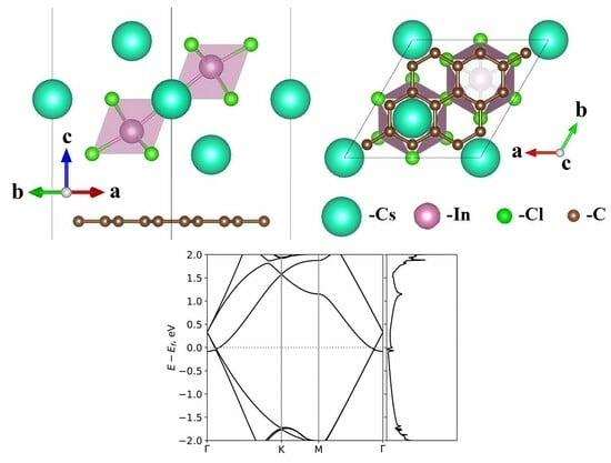
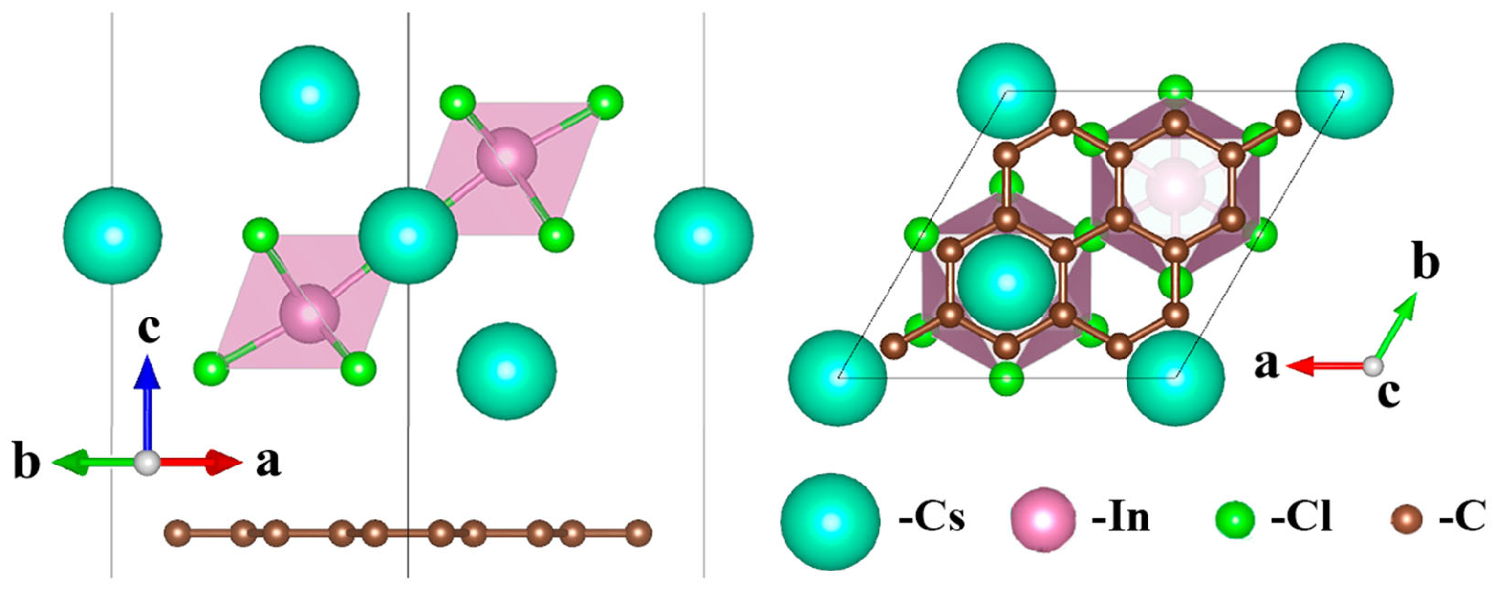
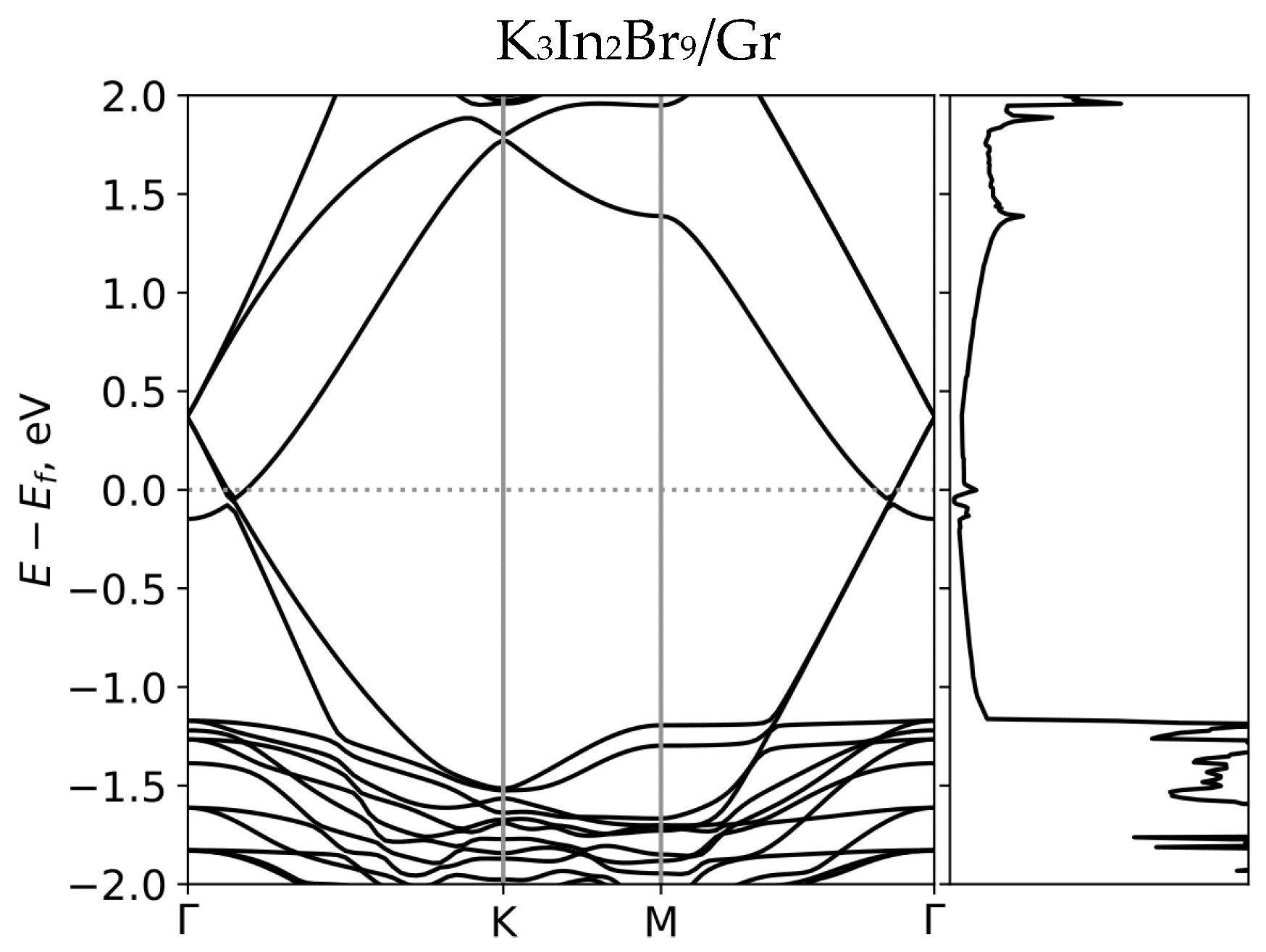
3. Results and Discussion

Among the various perovskites, In-based A3In2X9 perovskites can be distinguished, since they have the highest electron mobility and have a tunable band gap, which can change several times depending on the choice of halogen atoms [2]. Sb-based perovskites also deserve attention, since advances have been made in the synthesis of their <111>-oriented configurations [36,45]. In the presented study, monolayers A3In2X9 (A = Cs, Rb, K; X = Cl, Br) and A3Sb2X9 (A = Cs, Rb; X = Cl, Br) with hexagonal symmetry are analyzed (Figure 1). The unit cell of such perovskites consists of two halogen octahedrons interconnected by a common chlorine atom; inside the octahedra, there is an In/Sb atom. In the optimized cell, a displacement of metal atoms from the center of the halogen octahedron is observed. The observed displacement of metal atoms from the octahedral center is related to the structural features of the studied compound. This occurs precisely because we are examining a low-dimensional compound (quasi-two-dimensional crystal) rather than a bulk “three-dimensional” crystal. In quasi-two-dimensional structures, the spatial distribution of chemical bonds and interactions differs significantly from bulk materials. For instance, the environment of edge atoms at the boundary differs from the corresponding environment in a bulk system. This leads to a redistribution of electron density, which causes structural distortions—in our case, the observed displacement of metal atoms from the centers of octahedral positions. This effect is not related to the size of the unit cell and is also observed for larger supercells. This feature is confirmed by other independent studies, see reference [2]. In such a structure, it is possible to distinguish two types of B-X bonds—bridging and terminal ones (Figure 2). Bridging bonds are always longer than terminal ones. Optimized lattice constants are given in Table 1. A comparison of the results with other studies showed that the lattice constants are in good agreement. The maximum deviation from other studies was 1.1% for Cs3Sb2Br9.
To calculate the Goldschmidt tolerance factor t, we used Shannon ionic radii [30]. The K3In2Br9 has the lowest tolerance factor t = 0.907, and Cs3Sb2Cl9 has the highest one t = 0.997 (see Table 1). The octahedral factor for A3In2Cl9 is equal to 0.442. The A3Sb2Br9 structure has the lowest octahedral factor μ = 0.388. Therefore, all perovskites considered are theoretically stable.
Calculations of the electron band structures and density of states (DOS) were carried out. The band structure and DOS of all compounds studied in this work are given in the Supplementary Materials (see Figure S1). All of the considered perovskite structures exhibit semiconductor properties. The calculated values of the band gaps are given in Table 1. Sb-based perovskites possess the largest band gap among all considered perovskites.
Calculations show that Cs3Sb2Cl9, Rb3Sb2Cl9, and Rb3Sb2Br9 have an indirect band gap; the remaining perovskites are direct-gap semiconductors. All considered perovskites have CBM (conduction band minimum) at the Г point, but VBM (valence band maximum) is located on the Г-K path. The band structures of bulk Cs3Sb2X9 have been previously described in detail [47]. In such structures, s-p interaction is observed in the valence band, which is responsible for the formation of an antibonding orbital. In our study, a similar effect is observed for two-dimensional Sb-based perovskites. It has been determined that the contribution at the Fermi level is mainly associated with the p-orbital of the halogen and the s-orbital of antimony, with halogens having a different contribution. The contribution of central halogen atoms (connected to Sb by terminal bonds) is the most significant. As the antimony atom shifts from the center of the octahedron, the overlap changes, leading to a shift in the valence band maximum. As a result, some structures exhibit an indirect bandgap. To confirm this, we modeled a unit cell where the antimony atom remains at the center of the halogen octahedron, with atomic positions kept unrelaxed (Figure S8). The band structure of this configuration differs slightly, primarily due to the shift in the conduction band minimum and the valence band maximum, resulting in the transition to an indirect bandgap (Figure S9). A similar explanation for the formation of direct and indirect bandgaps has been demonstrated for three-dimensional Cs3Sb2X9 (X = Cl, Br), where the primary factor behind this transition is the X-Sb-X bond angle between terminal halogens [10].
Figure 3 shows the electronic band structure and the density of states for the perovskite Cs3In2Cl9, which is a direct band gap semiconductor. All considered, perovskites have a Dirac cone at the K-point. Among the electronic features of In-based perovskites, one can note the shift in the Dirac point above the Fermi level in the conduction band, while in Sb-based perovskites, the Dirac point shifts below the Fermi level in the valence band.
Next, we considered the situation where a graphene monolayer was deposited on the A3B2X9 monolayer. Graphene is held on perovskite by van der Waals forces (Figure 4), the characteristic distance between graphene and perovskite is ~3.5 Å.
The lattice constants of the considered perovskites are about 3 times greater than the lattice constant of graphene. The exception is Rb3In2Cl9 and K3In2Cl9 perovskites. These structures are stretched because their lattice constants are less than three times the lattice constant of graphene. The covalent bonds in graphene are much stronger, so the structure of perovskite is deformed. The K3In2Cl9 system has a larger tensile deformation, which increases the lattice constant by 1.64%. On the other hand, the reduction in graphene lattice is only ~0.22%. As a result of stretching, a decrease in the height of the structure along the c-axis is observed, simultaneously with an increase in the length of the B-X bonds. Moreover, the stretching of terminal bonds predominates. The greatest compressive strain is observed in the Cs3Sb2Br9 system. The lattice constant decreases by 7.7%, while at the same time, the graphene lattice stretches only by 0.73%. The greatest compression deformation is experienced by bridge bonds, while terminal bonds are practically not deformed. Terminal bonds in chlorine perovskite lead to a slight elongation of the bonds as a result of compression. Some electronic and geometric characteristics of composites based on perovskite and graphene are given in Table 2.
The lattice constant of most of the considered perovskites is about three times greater than the lattice constant of graphene, then at Г point on the k-path, the Dirac cone of graphene is observed due to the band folding [48]. In-based perovskites have a downshifting Fermi level relative to the Dirac point in graphene (Figure 5). When materials come into contact, their chemical potentials (Fermi levels) align. Since the initial Fermi level of graphene is higher than the Fermi level of the perovskite, charge transfer occurs from graphene to the perovskite. The conduction band of the perovskite begins to fill, while the Fermi level of graphene decreases. As a result of this process, a state is established corresponding to a shift in the Dirac cone of graphene (Figure S3).
The highest downshifting Fermi level possesses the electronic structure K3In2Br9, which is 0.364 eV. On the other hand, in the Sb-based perovskites, there is no shift in the Fermi level (see Figure S2 in Supplementary Materials).

4. Conclusions

In the presented study it was established that A3B2X9 perovskites are semiconductors, and various cations and anions allow the bandgap to be tuned. We investigated the possibility of depositing graphene on a perovskite monolayer. Graphene has stronger covalent bonds, which lead to the perovskite deformation in A3B2X9/Gr structures. The B-X bonds in perovskite have different sensitivity to deformation. Bridging bonds have larger deformation due to compressive strain than terminal bonds. At the same time, terminal bonds have larger deformation due to tensile strain.
For the In-based perovskite–graphene composite, a downshifting of the Fermi level by ~300 meV is observed; on the other hand, the Sb-based composite does not show such a change in electronic structure. The K3In2Br9 perovskite has the highest downshifting of the Fermi level. This property can be applied to the creation of new optoelectronic devices [49,50] or in hybrid supercapacitors [51].
The obtained results can be used further in combination with machine learning methods for predicting the properties of new perovskite–graphene composites. Machine learning algorithms are now actively used for predicting the atomic structure of quasi-two-dimensional materials, including perovskites, and their properties, such as band gap [52], mobility [53], thermoelectric properties [54], structural stability [55], etc. We also plan to use these approaches in our future studies.

Supplementary Materials

The following supporting information can be downloaded at: https://www.mdpi.com/article/10.3390/colloids9020023/s1, Figure S1: Electronic band structure and density of electronic states of different A3B2X9 perovskites; Figure S2: Electronic band structure and density of electronic states of different composites built from perovskite and graphene A3B2X9/Gr; Figure S3: Partial density of electronic states of different composites built from perovskite and graphene A3B2X9/Gr; Figure S4: Gr supercell (3 × 3); Figure S5: Gr supercell (3 × 3) electronic band structure and density of electronic states; Figure S6: Relaxing of 2 × 2 supercell Cs3In2Cl9/Gr; Figure S7: Electronic band structure and density of electronic states of 2 × 2 supercell Cs3In2Cl9/Gr; Figure S8: Not relaxing Cs3Sb2Cl9 unit cell; Figure S9: Electronic band structure and density of electronic states of not relaxing Cs3Sb2Cl9 unit cell.

Author Contributions

Conceptualization, L.Z. and M.M.; methodology, L.Z. and K.G.; software, L.Z., S.K. and P.K.; validation, K.G., M.M. and K.K.; formal analysis, K.K. and P.K.; investigation, L.Z. and K.K.; resources, M.M.; data curation, S.K., P.K. and K.G.; writing—original draft preparation, L.Z.; writing—review and editing, K.G., M.M. and P.K.; visualization, P.K.; supervision, M.M.; project administration, M.M.; funding acquisition, K.K. All authors have read and agreed to the published version of the manuscript.

Funding

The presented study was supported by the Ministry of Science and Higher Education of the Russian Federation, project FSWU−2024−0014.

Data Availability Statement

The data presented in this study are available in the Supplementary Materials.

Acknowledgments

Konstantin Grishakov, Konstantin Katin, and Mikhail Maslov thank the DSEPY-RI for the provided computing resources and comprehensive support of the presented study.

Conflicts of Interest

The authors declare no conflicts of interest.

References

  1. Li, X.; Gao, X.; Zhang, X.; Shen, X.; Lu, M.; Wu, J.; Shi, Z.; Colvin, V.L.; Hu, J.; Bai, X.; et al. Lead-Free Halide Perovskites for Light Emission: Recent Advances and Perspectives. Adv. Sci. 2021, 8, 2003334. [Google Scholar] [CrossRef] [PubMed]
  2. Luo, Q.; Su, L.; Lu, Y.; Fang, L.; Shu, H.; Cao, D.; Chen, X. Computational Screening of 2D All-Inorganic Lead-Free Halide Perovskites A3B2X9 for Photovoltaic and Photocatalytic Applications. Adv. Theory Simul. 2024, 7, 2300988. [Google Scholar] [CrossRef]
  3. Zhao, S.; Lan, C.; Li, H.; Zhang, C.; Ma, T. Aurivillius Halide Perovskite: A New Family of Two-Dimensional Materials for Optoelectronic Applications. J. Phys. Chem. C 2020, 124, 1788–1793. [Google Scholar] [CrossRef]
  4. Shao, M.; Bie, T.; Yang, L.; Gao, Y.; Jin, X.; He, F.; Zheng, N.; Yu, Y.; Zhang, X. Over 21% Efficiency Stable 2D Perovskite Solar Cells. Adv. Mater. 2022, 34, 2107211. [Google Scholar] [CrossRef]
  5. Liu, C.; Zhao, G.; Hu, T.; Chen, Y.; Cao, S.; Bellaiche, L.; Ren, W. Ferromagnetism, Jahn-Teller effect, and orbital order in the two-dimensional monolayer perovskite Rb2CuCl4. Phys. Rev. B 2021, 104, L241105. Available online: https://link.springer.com/article/10.1007/s12596-024-01819-9#citeas (accessed on 1 April 2025).
  6. Yang, Y.; Lou, F.; Xiang, H. Cooperative Nature of Ferroelectricity in Two-Dimensional Hybrid Organic-Inorganic Perovskites. Nano Lett. 2021, 21, 3170–3176. [Google Scholar] [CrossRef]
  7. Ma, K.; Li, X.; Yang, F.; Liu, H. Lead Leakage of Pb-Based Perovskite Solar Cells. Coatings 2023, 13, 1009. [Google Scholar] [CrossRef]
  8. Su, P.; Liu, Y.; Zhang, J.; Chen, C.; Yang, B.; Zhang, C.; Zhao, X. Pb-Based Perovskite Solar Cells and the Underlying Pollution behind Clean Energy: Dynamic Leaching of Toxic Substances from Discarded Perovskite Solar Cells. J. Phys. Chem. Lett. 2020, 11, 2812–2817. [Google Scholar] [CrossRef]
  9. Guo, W.H.; Shi, J.-J.; Zhu, Y.-H.; Wu, M.; Du, J.; Cen, Y.-L.; Liu, S.-M.; Han, S.-P. Two-Dimensional 111-Type in -Based Halide Perovskite Cs3In2X9 (X=Cl, Br, I) with Optimal Band Gap for Photovoltaics and Defect-Insensitive Blue Emission. Phys. Rev. Appl. 2020, 13, 024031. [Google Scholar] [CrossRef]
  10. Pradhan, A.; Jena, M.K.; Samal, S.L. Understanding of the Band Gap Transition in Cs3Sb2Cl9- xBrx: Anion Site Preference-Induced Structural Distortion. ACS Appl. Energy Mater. 2022, 5, 6952–6961. [Google Scholar] [CrossRef]
  11. Pradhan, A.; Sahoo, S.C.; Sahu, A.K.; Samal, S.L. Effect of Bi Substitution on Cs3Sb2Cl9: Structural Phase Transition and Band Gap Engineering. Cryst. Growth Des. 2020, 20, 3386–3395. [Google Scholar] [CrossRef]
  12. Wang, X.D.; Miao, N.-H.; Liao, J.-F.; Li, W.-Q.; Xie, Y.; Chen, J.; Sun, Z.-M.; Chen, H.-Y.; Kuang, D.-B. The top-down synthesis of single-layered Cs4CuSb2Cl12 halide perovskite nanocrystals for photoelectrochemical application. Nanoscale 2019, 11, 5180–5187. [Google Scholar] [CrossRef] [PubMed]
  13. Zhang, J.; Yang, Y.; Deng, H.; Farooq, U.; Yang, X.; Khan, J.; Tang, J.; Song, H. High Quantum Yield Blue Emission from Lead-Free Inorganic Antimony Halide Perovskite Colloidal Quantum Dots. ACS Nano 2017, 11, 9294–9302. [Google Scholar] [CrossRef] [PubMed]
  14. Kalesaki, E.; Boneschanscher, M.P.; Geuchies, J.; Delerue, C.; Delerue, C.; Smith, C.M.; Evers, W.; Allan, G.; Altantzis, T.; Bals, S.; et al. Preparation and Study of 2-D Semiconductors with Dirac Type Bands due to the Honeycomb Nanogeometry, in Physics. In Simulation, and Photonic Engineering of Photovoltaic Devices III, Proceedings of the SPIE Photonics West, San Francisco, CA, USA, 1–6 February 2014; SPIE: Bellingham, WC, USA, 2014; p. 898107. [Google Scholar] [CrossRef]
  15. Louie, S.G.; Park, C.H. Making massless dirac fermions from a patterned two-dimensional electron gas. Nano Lett. 2009, 9, 1793–1797. [Google Scholar] [CrossRef]
  16. Li, Z.; Han, Y.; Qiao, Z. Large-Gap Quantum Anomalous Hall Effect in Monolayer Halide Perovskite. Phys. Rev. B 2021, 104, 205401. [Google Scholar] [CrossRef]
  17. Chen, X.; Liu, L.; Shen, D. A simple rule for finding Dirac cones in bilayered perovskites. Chin. Phys. B 2019, 28, 077106. [Google Scholar] [CrossRef]
  18. Guo, S.; Bu, K.; Li, J.; Hu, Q.; Luo, H.; He, Y.; Wu, Y.; Zhang, D.; Zhao, Y.; Yang, W.; et al. Enhanced Photocurrent of All-Inorganic Two-Dimensional Perovskite Cs2PbI2Cl2 via Pressure-Regulated Excitonic Features. J. Am. Chem. Soc. 2021, 143, 2545–2551. [Google Scholar] [CrossRef]
  19. Saffari, M.; Soleimani, H.R.; Tagani, M.B. Quantum confinement and strain effects on the low-dimensional all-inorganic halide Cs2XI2Cl2 (X= Pb, Sn) perovskites: A theoretical approach for modulating electronic and optical properties. Phys. E Low-Dimens. Syst. Nanostructures 2020, 124, 114226. [Google Scholar] [CrossRef]
  20. Hwang, J.; Feng, Z.; Charles, N.; Wang, X.R.; Lee, D.; Stoerzinger, K.A.; Muy, S.; Rao, R.R.; Lee, D.; Jacobs, R.; et al. Tuning perovskite oxides by strain: Electronic structure, properties, and functions in (electro)catalysis and ferroelectricity. Mater. Today 2019, 31, 100–118. [Google Scholar] [CrossRef]
  21. Torma, A.J.; Li, W.; Zhang, H.; Tu, Q.; Klepov, V.V.; Brennan, M.C.; McCleese, C.L.; Krzyaniak, M.D.; Wasielewski, M.R.; Katan, C.; et al. Interstitial Nature of Mn2+ Doping in 2D Perovskites. ACS Nano 2021, 15, 20550–20561. [Google Scholar] [CrossRef]
  22. Liu, G.; Kong, L.; Guo, P.; Stoumpos, C.C.; Hu, Q.; Liu, Z.; Cai, Z.; Gosztola, D.J.; Mao, H.-K.; Kanatzidis, M.G.; et al. Two Regimes of Bandgap Red Shift and Partial Ambient Retention in Pressure-Treated Two-Dimensional Perovskites. ACS Energy Lett. 2017, 2, 2518–2524. [Google Scholar] [CrossRef]
  23. Tan, R.; Zou, C.; Pan, K.; Zou, D.; Liu, Y. Enhancing thermoelectric properties of BiCuSeO via uniaxial compressive strain: First-principles calculations. J. Alloys Compd. 2018, 743, 610–617. [Google Scholar] [CrossRef]
  24. Wang, M.; Hou, T.-P.; Wu, K.-M.; Lin, H.-F. Graphene/Cs2PbI2Cl2 van der Waals heterostructure with tunable Schottky barriers and contact types. J. Appl. Phys. 2022, 132, 165101. [Google Scholar] [CrossRef]
  25. Sun, Y.; Morice, C.; Garrot, D.; Weil, R.; Watanabe, K.; Taniguchi, T.; Monteverde, M.; Chepelianskii, A.D. Quantum Transport and Spectroscopy of 2D Perovskite/Graphene Heterostructures. Adv. Elect. Mater. 2024, 10, 2400211. [Google Scholar] [CrossRef]
  26. Hu, J.; Ji, G.; Ma, X.; He, H.; Huang, C. Probing interfacial electronic properties of graphene/CH3NH3PbI3 heterojunctions: A theoretical study. Appl. Surf. Sci. 2018, 440, 35–41. [Google Scholar] [CrossRef]
  27. Zibouche, N.; Volonakis, G.; Giustino, F. Graphene Oxide/Perovskite Interfaces for Photovoltaics. J. Phys. Chem. C 2018, 122, 16715–16726. [Google Scholar] [CrossRef]
  28. Agresti, A.; Pescetelli, S.; Taheri, B.; Del Rio Castillo, A.E.; Cinà, L.; Bonaccorso, F.; Di Carlo, A. Graphene–Perovskite Solar Cells Exceed 18% Efficiency: A Stability Study. ChemSusChem 2016, 9, 2609–2619. [Google Scholar] [CrossRef]
  29. Zhao, L.; Tian, H.; Silver, S.H.; Kahn, A.; Ren, T.-L.; Rand, B.P. Ultrasensitive Heterojunctions of Graphene and 2D Perovskites Reveal Spontaneous Iodide Loss. Joule 2018, 2, 2133–2144. [Google Scholar] [CrossRef]
  30. Shannon, R.D.; Prewitt, C.T. Revised values of effective ionic radii. Acta Crystallogr. B Struct. Crystallogr. Cryst. Chem. 1970, 26, 1046–1048. [Google Scholar] [CrossRef]
  31. Tiwari, D.; Hutter, O.S.; Longo, G. Chalcogenide perovskites for photovoltaics: Current status and prospects. J. Phys. Energy 2021, 3, 034010. [Google Scholar] [CrossRef]
  32. Jacobsson, T.J.; Pazoki, M.; Hagfeldt, A.; Edvinsson, T. Goldschmidt’s Rules and Strontium Replacement in Lead Halogen Perovskite Solar Cells: Theory and Preliminary Experiments on CH3NH3SrI3. J. Phys. Chem. C 2015, 119, 25673–25683. [Google Scholar] [CrossRef]
  33. Xia, M.; Yuan, J.-H.; Niu, G.; Du, X.; Yin, L.; Pan, W.; Luo, J.; Li, Z.; Zhao, H.; Xue, K.-H.; et al. Unveiling the Structural Descriptor of A3B2X9 Perovskite Derivatives toward X-Ray Detectors with Low Detection Limit and High Stability. Adv. Funct. Mater. 2020, 30, 1910648. [Google Scholar] [CrossRef]
  34. Kim, S.-Y.; Yun, Y.; Shin, S.; Lee, J.H.; Heo, Y.-W.; Lee, S. Wide range tuning of band gap energy of A3B2X9 perovskite-like halides. Scr. Mater. 2019, 166, 107–111. [Google Scholar] [CrossRef]
  35. Peresh, E.Y.; Sidei, V.I.; Zubaka, O.V.; Stercho, I.P. K2(Rb2,Cs2,Tl2)TeBr6(I6) and Rb3(Cs3)Sb2(Bi2)Br9(I9) perovskite compounds. Inorg. Mater. 2011, 47, 208–212. [Google Scholar] [CrossRef]
  36. Saparov, B.; Hong, F.; Sun, J.-P.; Duan, H.-S.; Meng, W.; Cameron, S.; Hill, I.G.; Yan, Y.; Mitzi, D.B. Thin-Film Preparation and Characterization of Cs3Sb2I9: A Lead-Free Layered Perovskite Semiconductor. Chem. Mater. 2015, 27, 5622–5632. [Google Scholar] [CrossRef]
  37. Giannozzi, P.; Baroni, S.; Bonini, N.; Calandra, M.; Car, R.; Cavazzoni, C.; Ceresoli, D.; Chiarotti, G.L.; Cococcioni, M.; Dabo, I.; et al. Quantum Espresso: A modular and open-source software project for quantum simulations of materials. J. Phys. Condens. Matter. 2009, 21, 395502. [Google Scholar] [CrossRef]
  38. Giannozzi, P.; Andreussi, O.; Brumme, T.; Bunau, O.; Nardelli, M.B.; Calandra, M.; Car, R.; Cavazzoni, C.; Ceresoli, D.; Cococcioni, M.; et al. Advanced capabilities for materials modelling with Quantum ESPRESSO. J. Phys. Condens. Matter. 2017, 29, 465901. [Google Scholar] [CrossRef]
  39. Perdew, J.P.; Burke, K.; Ernzerhof, M. Generalized Gradient Approximation Made Simple. Phys. Rev. Lett. 1996, 77, 3865–3868. [Google Scholar] [CrossRef]
  40. Blöchl, P.E. Projector augmented-wave method. Phys. Rev. B 1994, 50, 17953–17979. [Google Scholar] [CrossRef]
  41. Kresse, G.; Joubert, D. From ultrasoft pseudopotentials to the projector augmented-wave method. Phys. Rev. B 1999, 59, 1758–1775. [Google Scholar] [CrossRef]
  42. Grimme, S.; Antony, J.; Ehrlich, S.; Krieg, H. A consistent and accurate ab initio parametrization of density functional dispersion correction (DFT-D) for the 94 elements H-Pu. J. Chem. Phys. 2010, 132, 154104. [Google Scholar] [CrossRef] [PubMed]
  43. Monkhorst, H.J.; Pack, J.D. Special points for Brillouin-zone integrations. Phys. Rev. B 1976, 13, 5188–5192. [Google Scholar] [CrossRef]
  44. Blöchl, P.E.; Jepsen, O.; Andersen, O.K. Improved tetrahedron method for Brillouin-zone integrations. Phys. Rev. B 1994, 49, 16223–16233. [Google Scholar] [CrossRef] [PubMed]
  45. Lu, C.; Itanze, D.S.; Aragon, A.G.; Ma, X.; Li, H.; Ucer, K.B.; Hewitt, C.; Carroll, D.L.; Williams, R.T.; Qiu, Y.; et al. Synthesis of lead-free Cs3Sb2Br9 perovskite alternative nanocrystals with enhanced photocatalytic CO2 reduction activity. Nanoscale 2020, 12, 2987–2991. [Google Scholar] [CrossRef]
  46. Long, Y.; Zhang, H.; Cheng, X. Stability, electronic structure, and optical properties of lead-free perovskite monolayer Cs3B2X9 (B = Sb, Bi; X = Cl, Br, I) and bilayer vertical heterostructure Cs3B2X9/Cs3B2’X9 (B,B’ = Sb, Bi; X = Cl, Br, I). Chin. Phys. B 2022, 31, 027102. [Google Scholar] [CrossRef]
  47. Liu, Y.-L.; Yang, C.-L.; Wang, M.-S.; Ma, X.-G.; Yi, Y.-G. Theoretical insight into the optoelectronic properties of lead-free perovskite derivatives of Cs3Sb2X9 (X = Cl, Br, I). J. Mater. Sci. 2019, 54, 4732–4741. [Google Scholar] [CrossRef]
  48. Laref, A.; Ahmed, A.; Bin-Omran, S.; Luo, S.J. First-principle analysis of the electronic and optical properties of boron and nitrogen doped carbon mono-layer graphenes. Carbon 2015, 81, 179–192. [Google Scholar] [CrossRef]
  49. Singh, A.K.; Singh, A.K.; Sinha, S.R.P. Fermi-Level Modulation of Chemical Vapor Deposition-Grown Monolayer Graphene via Nanoparticles to Macromolecular Dopants. ACS Omega 2022, 7, 744–751. [Google Scholar] [CrossRef]
  50. Adhikari, S.; Perello, D.J.; Biswas, C.; Ghosh, A.; Van Luan, N.; Park, J.; Yao, F.; Rotkinac, S.V.; Lee, Y.H. Determining the Fermi level by absorption quenching of monolayer graphene by charge transfer doping. Nanoscale 2016, 8, 18710–18717. [Google Scholar] [CrossRef]
  51. Madito, M.J. Correlation of the Graphene Fermi-Level Shift and the Enhanced Electrochemical Performance of Graphene-Manganese Phosphate for Hybrid Supercapacitors: Raman Spectroscopy Analysis. ACS Appl. Mater. Interfaces 2021, 13, 37014–37026. [Google Scholar] [CrossRef]
  52. Hui, Z.; Wang, M.; Chen, J.; Yin, X.; Yue, Y.; Lu, J. Predicting photovoltaic parameters of perovskite solar cells using machine learning. J. Phys. Condens. Matter. 2024, 36, 355901. [Google Scholar] [CrossRef] [PubMed]
  53. Rashid, M.A.M.; Lee, S.; Kim, K.H.; Kim, J.; Jeong, K. Machine Learning Approach for Predicting the Hole Mobility of the Perovskite Solar Cells. Adv. Theory Sims 2024, 7, 2300978. [Google Scholar] [CrossRef]
  54. He, Z.; Peng, J.; Lei, C.; Xie, S.; Zou, D.; Liu, Y. Prediction of superior thermoelectric performance in unexplored doped-BiCuSeO via machine learning. Mater. Des. 2023, 229, 111868. [Google Scholar] [CrossRef]
  55. Mammeri, M.; Bencherif, H.; Dehimi, L.; Hajri, A.; Sasikumar, P.; Syed, A.; AL-Shwaiman, H.A. Stability forecasting of perovskite solar cells utilizing various machine learning and deep learning techniques. J. Opt. 2024. [Google Scholar] [CrossRef]
Figure 1. The monolayer of the Cs3In2Cl9 perovskite.
Colloids 09 00023 g001
Figure 2. The bond structure in the halogen octahedron. Bridging bonds form B-X-B connections and are located in the center of such a structure. The structure has six bridging and six terminal bonds. Line shows the unit cell boundary.
Colloids 09 00023 g002
Figure 3. Electronic band structure and density of electronic states of Cs3In2Cl9. Perovskite has a direct bandgap at Г point.
Colloids 09 00023 g003
Figure 4. The atomic structure of the composite built from the graphene and perovskite layers.
Colloids 09 00023 g004
Figure 5. Electronic band structure and density of electronic states of K3In2Br9/Gr.
Colloids 09 00023 g005
Table 1. Characteristics of the A3B2X9 perovskite, where t is the Goldschmidt tolerance factor, and a, b, and c are the lattice parameters, μ is the octahedral factor. Values obtained in other studies and the corresponding references to these studies are given in parentheses for comparison.
Compound μ ta = b, Åc, ÅBand Gap, eV
(Direct/Indirect)
B-X, Terminal Bond, ÅB-X, Bridging Bond, Å
Cs3In2Cl90.4420.9737.457 (7.45 [9])6.0572.00 (D)2.4482.770
Cs3In2Br90.4080.9677.848 (7.86 [9])6.2721.18 (D)2.6012.955
Rb3In2Cl90.4420.9407.328 (7.327 [2])5.8192.04 (D)2.4392.755
Rb3In2Br90.4080.9277.744 (7.752 [2])6.2351.16 (D)2.5912.945
Cs3Sb2Cl90.4200.9977.712 (7.715 [46])6.3122.76 (D)2.5192.869
Cs3Sb2Br90.3880.9728.026 (7.935 [46])6.6932.32 (I)2.6793.014
Rb3Sb2Cl90.4200.9717.561 (7.561 [2])6.3202.73(I)2.5132.859
Rb3Sb2Br90.3880.9577.906 (7.848 [35])6.6922.27 (I)2.6713.008
K3In2Cl90.4420.9337.261 (7.264 [2])5.7752.05 (D)2.4302.751
K3In2Br90.4080.9077.693 (7.693 [2])6.1921.16 (D)2.5822.946
Table 2. Geometry and electronic characteristics of the A3B2X9/Gr composite. Parameter d is the distance between the perovskite and graphene. Average values of the length of terminal and bridge bonds are presented.
Compounda = b, Åc, Åd, ÅDownshifting of the Fermi Level, eVB-X, Terminal Bond, ÅB-X, Bridging Bond, ÅCompound
Cs3In2Cl97.4036.0713.6100.3262.4502.755Cs3In2Cl9
Cs3In2Br97.4446.5633.6600.3282.5922.877Cs3In2Br9
Rb3In2Cl97.3905.7933.5480.2532.4452.753Rb3In2Cl9
Rb3In2Br97.4296.3933.5780.3412.5832.871Rb3In2Br9
Cs3Sb2Cl97.4186.4043.579-2.5222.823Cs3Sb2Cl9
Cs3Sb2Br97.4526.9653.636-2.6642.941Cs3Sb2Br9
Rb3Sb2Cl97.4056.2963.488-2.5192.814Rb3Sb2Cl9
Rb3Sb2Br97.4376.8773.560-2.6572.931Rb3Sb2Br9
K3In2Cl97.3825.6933.4590.2792.4402.754K3In2Cl9
K3In2Br97.4196.3163.5450.3642.5752.871K3In2Br9
Disclaimer/Publisher’s Note: The statements, opinions and data contained in all publications are solely those of the individual author(s) and contributor(s) and not of MDPI and/or the editor(s). MDPI and/or the editor(s) disclaim responsibility for any injury to people or property resulting from any ideas, methods, instructions or products referred to in the content.

