Abstract
High-quality, reproducible tip coatings are essential for minimizing faradaic currents in electrochemical scanning tunneling microscopy (EC-STM), especially during in situ and operando measurements. The variability inherent in manual coating methods, influenced by the operator’s skill and a lack of standardization, can lead to inconsistent results, increased research costs, and a greater workload. This study introduces an Automated Tip Coater (ATC) designed to automate and standardize the tip coating process. The ATC features a tip movement system using stepper motors, a rotation module with a DC motor, and a heating block based on a soldering iron. It is controlled by an Arduino development board, supported by motor drivers, and has a user-friendly interface with an OLED display and encoder. The ATC coating mechanism includes a redesigned plate with a reduced gap size and a milled tray to precisely control the amount of insulating material applied to the tip. A fast cyclic voltammetry test in a 0.1 M HClO4 electrolyte demonstrated that over 75% of ATC-coated tips achieved excellent insulation with leakage currents below ±50 pA—and 30% below ±10 pA—suitable for highly sensitive experiments. Further measurements with EC-STM using the newly coated tips investigated the electrochemical behavior of highly oriented pyrolytic graphite (HOPG), revealing detailed atomic structures under dynamic electrochemical conditions. The ATC significantly enhances reproducibility, reduces dependency on operator skills, and lowers research costs while improving the accuracy and reliability of EC-STM measurements.
1. Introduction
Electrochemical scanning tunneling microscopy (EC-STM) is a powerful technique that enables the study of various surface phenomena at the atomic level under electrochemical conditions [1,2,3]. This capability is crucial for advancing our understanding of dynamic processes in various fields, including electrocatalysis [4,5,6], corrosion [7,8], energy storage [9,10], and nanotechnology [11,12]. By enabling in situ and operando measurements, EC-STM allows researchers to observe real-time changes in the surface structure and composition during electrochemical reactions, providing insights that are essential for developing next-generation technologies in these areas [13,14].
Recent advancements in EC-STM have demonstrated the potential to identify electrocatalytically active sites with atomic precision by analyzing noise in the tunneling current [13,15,16,17,18,19,20,21,22,23,24,25,26]. By using this approach, it is possible to monitor catalytic sites during electrochemical reactions, offering insights into their stability and providing quantitative information related to the macroscopic onset potential, Tafel slope, and turnover frequency (TOF) with sub-nanometric spatial resolution, even for single-atom catalytic sites. This new method enables the determination of the nature, relative abundance, and specific activity of the sites where electrocatalytic processes occur, all at the atomic level. However, one of the major challenges in obtaining accurate and reliable EC-STM data is maintaining faradaic currents at negligible levels. These currents, which arise from electrochemical reactions at the tip due to the applied bias potential, can significantly interfere with the tunneling current, especially during in situ and operando measurements where dynamic changes in the electrochemical environment are prevalent.
Therefore, the EC-STM tips must be coated with a chemically and electrochemically inert insulating material, leaving only the apex exposed to the electrolyte [27]. Effective tip coatings markedly reduce unwanted faradaic leakage currents. Various insulating techniques have been developed, differing in the choice of coating materials and specialized equipment required. These methods include glass coating [28,29,30,31] followed by the sputter deposition of SiO [32], the application of cataphoretic paint [33,34], the thermal evaporation of silicon or magnesium oxides [35], and the use of waxes [36,37] or polymers such as nail varnish [38,39,40], epoxy resin [41,42,43], and silicon rubber [41,44]. Molten polymers [29,30,45,46] or Apiezon wax [47,48,49,50,51] are commonly selected for their straightforward use and excellent insulating properties [33]. However, the quality of tip coatings obtained using these techniques is often highly dependent on the operator’s manual skills, introducing variability that can range from well-insulated tips to those with inadequate or even complete insulation. Without the prior assessment of the tip coating quality, such irregularities can adversely impact the reliability of the EC-STM data, especially when an atomic-scale resolution is required but cannot be realized due to insufficient tip insulation.
Achieving the precision and consistency required in techniques such as EC-STM necessitates eliminating factors that compromise the integrity of results, particularly those associated with manual procedures like tip coating. In recent years, there has been a growing emphasis on automation and standardization in scientific research, driven by the need for reproducibility, efficiency, and a reduction in human errors [52]. The development of automated systems, such as the Automated Tip Coater (ATC) introduced in this study, represents a crucial step toward overcoming these challenges. By automating fundamental steps like tip coating, the ATC removes operator dependency and standardizes the process, aligning with the broader trend of enhancing experimental reproducibility and accuracy. The ATC uses molten polymers or Apiezon wax to provide a consistent insulating layer. Its key features include a precision tip movement system controlled by stepper motors, a rotational module driven by a DC motor, and a temperature-controlled heating block with a redesigned plate featuring a reduced gap size and a milled tray for the precise application of insulating material. The system is managed by an Arduino development board, with control software developed in C++ using PlatformIO for stand-alone operations. Furthermore, the ATC is user-friendly and requires minimal training, allowing users of all experience levels to achieve consistent results. Its modular design enables seamless adjustments to accommodate various EC-STM tip specifications—including tip diameter and length, as well as insulating material properties—ensuring the system can be tailored to the specific practices of any laboratory.
This study aims to address the challenges of achieving high-quality, reproducible tip coatings in EC-STM by developing the ATC. The primary objectives are to standardize the coating process, reduce operator-induced variability, and improve the reliability of EC-STM measurements under in situ and operando conditions. By achieving these goals, the study seeks to enhance the utility of EC-STM as a tool for investigating surface phenomena at the atomic scale, ultimately contributing to advancements in fields such as electrocatalysis, materials science, and energy storage.
2. Materials and Methods
2.1. Electrochemical Etching of W Tips
The STM tips were prepared by standard EC etching from a tungsten wire of 0.25 mm diameter in a 2 M KOH solution [53,54]. Briefly, the etching process involves using a platinum wire loop with a diameter of 6 mm that serves as the counter electrode. The tungsten wire is placed in the center of the Pt loop so that 7 mm of the W wire is below the horizontal plane of the Pt loop. The loop is then immersed in the electrolyte to suspend a thin lamella of electrolyte. A rectangular AC voltage of 8 Vpp and a frequency of 100 Hz is applied between the tungsten wire and the Pt wire loop. The etching process continues until the free end of the tungsten wire falls off into the Teflon container. The W tip is then rinsed with high-purity water and dried.
2.2. System Design and Architecture of the ATC
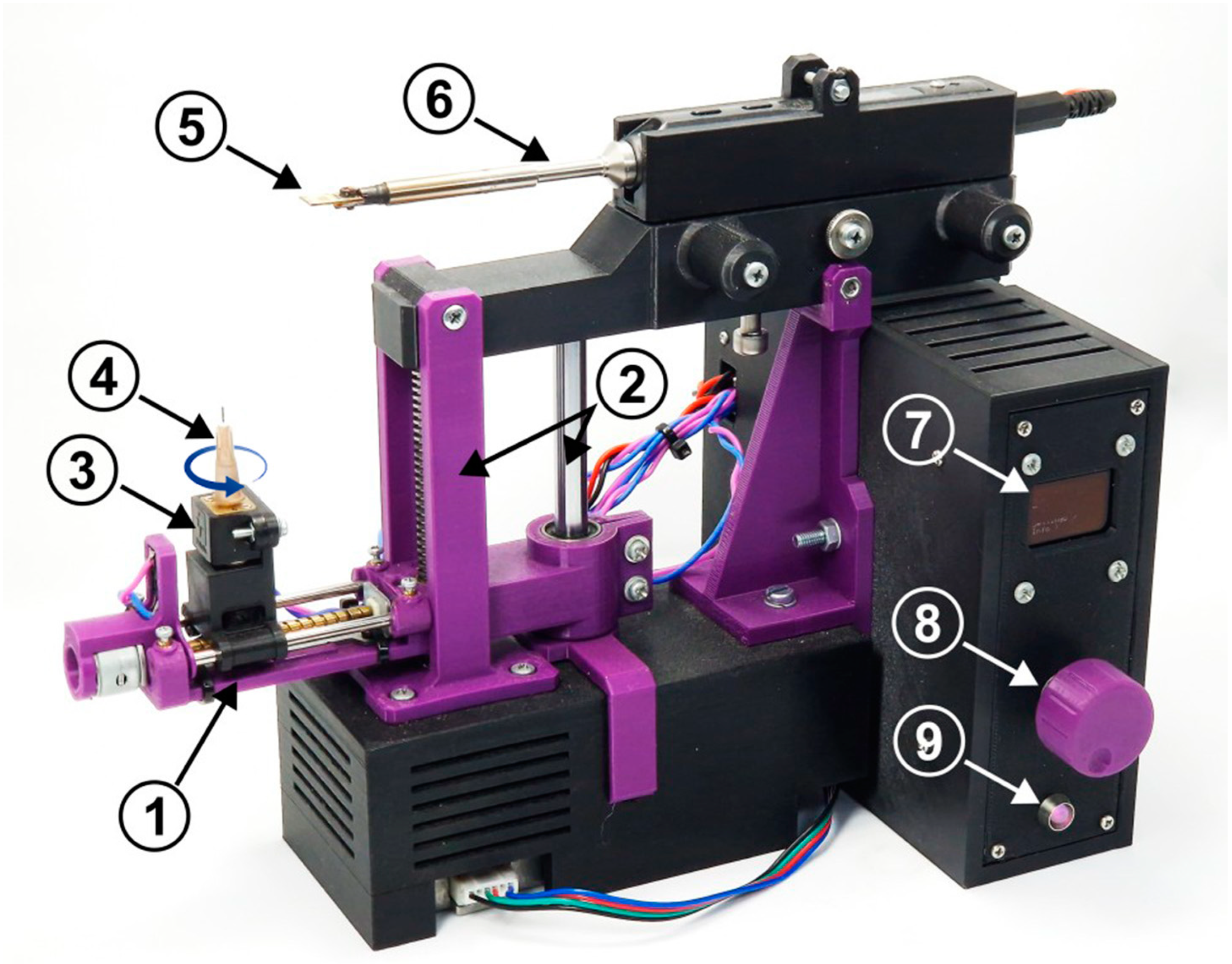
The ATC was developed with a focus on reliability, repeatability, and ease of use. A complete image of the working device is shown in Figure 1. The core design incorporates several key modules: a precise tip positioning system, a rotational module, and a temperature-controlled heating block with a redesign tray for melting insulating materials. The ATC is designed with a user-friendly interface, allowing researchers to configure all relevant parameters, including the immersion depth, coating duration, rotation speed, and horizontal and vertical movement speeds.

Figure 1.
Image of the ATC system with labeled components: (1) Horizontal movement module; (2) Vertical movement module; (3) Rotational module; (4) Tip holder; (5) Coating tray; (6) Heating module; (7) OLED display; (8) Encoder for user input; (9) RGB status indicator.
The mechanical design focuses on precise and controlled movements. Most of the components were made using 3D printing technology, providing flexibility in design iterations and rapid prototyping. The system includes vertical and horizontal movement modules, driven by precision stepper motors, that provide micron-level accuracy in tip positioning. The vertical motion is controlled by a Nema 17 stepper motor coupled with an 8 mm lead screw, enabling smooth and repeatable linear displacement. A smaller stepper motor, typically used in DVD drives, facilitates accurate lateral positioning. The incorporation of linear bearings in both systems minimizes friction and enhances stability, allowing for highly controlled tip immersion and withdrawal during the coating process.
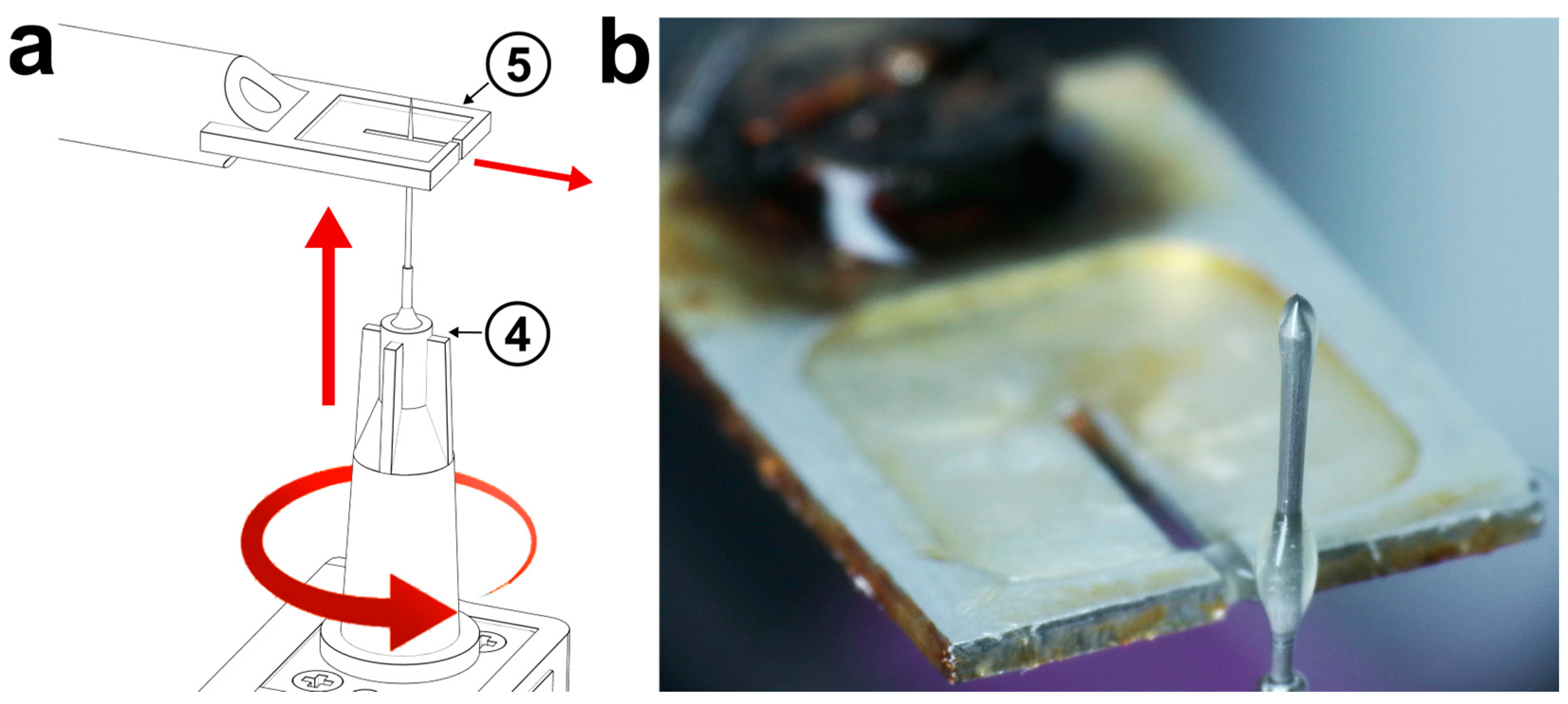
The key innovations that distinguish this device are the redesigned coating tray and the addition of a rotational module. The coating tray has been engineered with a narrow slit that is only 50 μm wider than the tip diameter (see Figure 2). Furthermore, the tray is milled to enhance the distribution and volume control of the insulating material within the cavity, which ensures that the correct amount of insulating material adheres to the tip, minimizing excess and resulting in a consistent insulation layer.
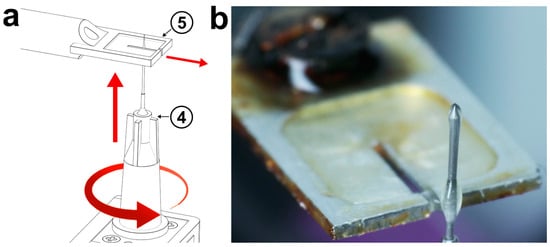
Figure 2.
(a) A 3D model illustrating the tip passing through the slit in the tray (5) during the coating process, with red arrows indicating the direction of movement (upward) and rotation. (b) Photograph showing the coated tip emerging from the tray after the insulation process.
The rotational module, powered by a DC motor, is another feature designed to achieve uniform coatings. This module includes a holder that secures the tip during the coating process while allowing it to rotate smoothly around its axis. The rotation speed and duration are fully adjustable to match the properties of the insulating material, ensuring an even coverage across the entire tip surface.
The durability and performance of coated tips are greatly influenced by the choice of insulating material. The system is compatible with various materials, including molten polymers and Apiezon wax, which are widely used for their known insulating properties and chemical resistance. In this study, we primarily used Pattex PTK1 hot melt glue sticks (Henkel, Germany), an Ethylene Vinyl Acetate Copolymer (EVA) adhesive with a softening temperature of 85 ± 5 °C. The heating block is based on a modified TS100 soldering iron, capable of reaching temperatures up to 400 °C with minimal hysteresis. The material is heated to the desired viscosity within the tray cavity, which is monitored in real-time through a temperature sensor, allowing precise adjustments as needed.
2.3. Tip Coating Process
The process of insulating the tips begins by depositing the insulating material into the tray cavity (5) (Figure 1 and Figure 2). During the heating phase, the tip holder (4) is positioned at the lower end, opposite the tray, allowing for the safe and secure placement of the tip in the holder. Once the insulating material reaches its melting point, it is evenly distributed within the tray cavity. Excess material is removed using a flat tool (e.g., a utility knife) swept across the edges surrounding the tray cavity, ensuring a consistent volume of applied insulating material. Any material leaking through the slit is also removed with the flat tool before the coating process begins.
Next, the tip holder is automatically moved beneath the tray containing the insulating material. By gradually passing through the slit from below, the tip is immersed in the insulating material (Figure 2). Depending on the type of insulating material used, the tip rotation can be initiated at one of three stages: (1) while passing through the slit, (2) immediately after passing through the slit, or (3) during withdrawal from the slit. These parameters can be adjusted by the user based on experience to achieve optimal coating coverage. After a few seconds, the platform returns to its initial position, allowing for the safe removal of the coated tip. This process is shown in videos 1 and 2, which are included in the online Supporting Information.
2.4. Cyclic Voltammetry of Coated Tips
The CV measurements in 0.1 M HClO4 electrolyte of the ATC-coated tips were carried out in a home-built three-electrode cell using a PocketPotentiostat developed by Matsubara [55]. Pt wires were used as counter and reference electrodes, placed less than 1 cm from the working electrode. The Pt quasi-reference electrode was calibrated with respect to RHE in argon-saturated 0.1 M HClO4. All potentials thereafter are quoted with respect to RHE at pH = 1. The electrochemical cell was placed in a Faraday cage to minimize noise introduced by electromagnetic interference, which is essential for picoelectrochemical measurements.
2.5. EC-STM Measurements
The EC-STM measurements were carried out using a home-built EC-STM working in a constant-current mode, as described in detail by Wilms et al. [56]. This system is enhanced with a high-speed ADC acquisition card (Texas Instruments) that captures data at a rate up to 640 kSps. It features six channels simultaneously recording signals from the EC-STM, including lateral piezo displacement, working electrode potential, and sample current. Channels allocated for the recording of tunneling current and z-axis tip displacement during forward and backward scans enable the acquisition of both current and topographical STM images.
All electrolytes were prepared using deionized water from a Millipore-Pure system (Merck, Burlington, MA, USA) with a specific resistance of 18.2 MΩ·cm and minimal organic impurities in the ppb range. Prior to use, the electrolytes were purged with argon gas for several hours. The chemicals used, obtained from Sigma-Aldrich (Saint Louis, MO, USA), were of the highest commercially available purity and were used without further purification.
The HOPG electrode (TipsNano, ZYB quality, mosaic spread: 0.8 ± 0.2°) was prepared through mechanical exfoliation of the topmost layers by adhesive tape. To prevent re-contamination of the surface, the HOPG was immediately mounted into the EC cell of the EC-STM and covered with a drop of degassed electrolyte.
All electrode potentials in the publication are referred to as an RHE reference electrode, while all tip bias potentials are reported with respect to the working electrode. Therefore, the bias voltage to the tip can be referred to as the RHE electrode in accordance with this equation:
where Ub vs. ref represents the bias applied to the tip versus the reference electrode, E denotes the electrode potential, and Ub is the bias versus working electrode potential [53].
Ub vs. ref = E + Ub
3. Results and Discussion
3.1. Visual Assessment of Tip Coating Quality
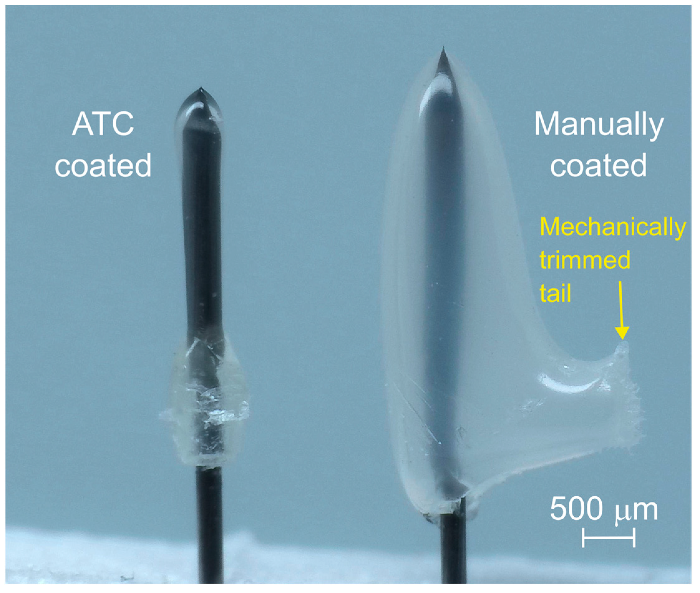
The quality of the coated tips was evaluated using a two-step process involving both optical inspection and electrochemical testing. The first step focused on assessing insulation continuity, uniformity, and coating thickness under an optical microscope (Figure 3). The results revealed that tips coated using the ATC displayed smooth and consistent insulation with minimal excess material. In contrast, manually coated tips often exhibited significant excess material, forming polymer tails that required mechanical trimming. These tails, resulting from the adhesive nature of the coating material, are a common issue in manual coating processes and can introduce variability in the insulation layer, particularly near the tip apex. This variability not only affects the reproducibility of EC-STM measurements but also increases the risk of damaging the insulation during the trimming process.
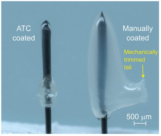
Figure 3.
Comparison of tip coatings produced by the ATC and manually. The ATC-coated tip (left) shows smooth and consistent insulation without excess material or polymer tails. In contrast, the manually coated tip (right) exhibits a significant excess of insulating material, forming a tail that requires mechanical trimming.
The ATC rotational module effectively addresses this issue by maintaining continuous rotation during the withdrawal phase of the coating process. By rotating the tip as it is withdrawn from the insulating material, the rotational module prevents the formation of polymer tails, ensuring a uniform and smooth coating without the need for further mechanical intervention (Figure 3). This automation of the coating process reduces the dependence on operator skill and eliminates a significant source of variability.
3.2. Electrochemical Testing of Coated Tips
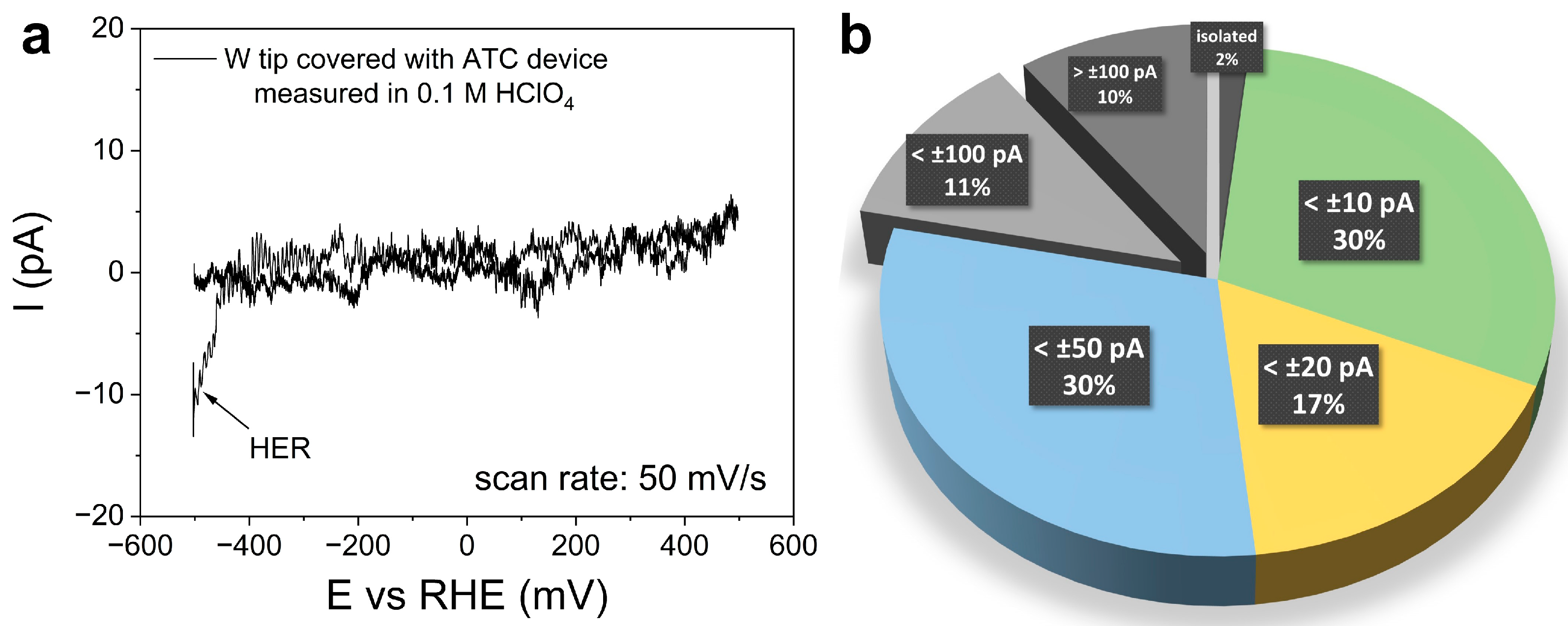
The second and most crucial phase of quality assessment involved conducting fast cyclic voltammetry (CV) tests to evaluate the electrochemical stability and insulation performance of the coated tips. In these tests, tungsten tips coated using the ATC were assessed in 0.1 M HClO4 at a scan rate of 50 mV/s within an electrode potential window of −500 mV to 500 mV. The relatively high scan rate was chosen to expedite the evaluation process, allowing multiple tips to be tested in a shorter timeframe.
Figure 4 presents two key outcomes: on the left, the CV curve of a coated tip, and on the right, the statistical analysis of the insulation performance across a total of 60 tips sourced from five independent batches (batch 1: 15 tips, batch 2: 12 tips, batch 3: 6 tips, batch 4: 9 tips, batch 5: 18 tips). The CV curve illustrates that the ATC-coated tip maintained a low leakage current within the range of ±10 pA, signifying effective insulation. The statistical analysis revealed that 30% of the tips exhibited leakage currents below ±10 pA, with an additional 30% maintaining leakage below ±50 pA. Furthermore, 17% of the tips showed leakage currents below ±20 pA, while only 10% exhibited currents exceeding ±100 pA, indicating minor defects. A small percentage (2%) were fully isolated, showing negligible current leakage. A contrasting trend emerges in the analysis of manually coated tips, as illustrated in Figure S2 of the Supporting Information. Among the 74 tips examined, 28% were fully isolated, while a significant 43% displayed leakage current exceeding ±100 pA. Notably, only 6% of tips recorded leakage current below ±10 pA, with an additional 2% maintaining leakage levels below ±20 pA. These results further highlight the effectiveness of the automated approach to tip coating employed by the ATC.
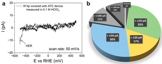
Figure 4.
(a) Typical CV curve recorded in 0.1 M HClO4 electrolyte for a W tip coated using the ATC. (b) Pie chart showing the percentage of coated tips with leakage currents below specific thresholds.
Understanding the role of insulation quality is key to determining the suitability of tips for diverse EC-STM experiments. The distribution shown in Figure 4b demonstrates that the ATC can produce tips suitable for a wide range of experimental needs, from general imaging to highly sensitive EC-STM measurements, especially with the bias tip potential kept constant versus sample potential.
The required level of tip insulation depends significantly on the specific type of EC-STM experiment being conducted. While high-resolution imaging of atomic structures can often be achieved with tips exhibiting leakage currents exceeding ±100 pA—by adjusting the bias voltage to match the open circuit potential of the tip and increasing the tunneling current setpoint—certain advanced measurements demand higher insulation quality.
For instance, experiments involving step or cyclic voltammetry (CV) potentiodynamic measurements and quasi-spectroscopy are particularly sensitive to leakage currents. In these techniques, the tip potential is varied over a range, and any leakage current can interfere with the accuracy of the measurements by introducing additional faradaic currents or disturbing the electrochemical equilibrium at the tip-sample interface. Therefore, tips with leakage currents below ±50 pA, ±20 pA, or even ±10 pA are preferred for such sensitive experiments.
By producing a significant proportion of tips with leakage currents below ±10 pA and ±20 pA, the ATC provides researchers with the ability to select tips based on the specific insulation quality required for their experiments, enhancing the versatility and reliability of EC-STM studies. This improvement not only elevates the quality of imaging and measurements but also reduces the frequency of tip replacement, thereby lowering operational costs.
Therefore, the performance of the ATC-coated tips at such a high scan rate is particularly notable, as EC-STM measurements are typically conducted at lower scan rates to minimize Faradaic current. Maintaining low leakage currents at 50 mV/s highlights the high-quality insulation provided by the ATC. It also demonstrates the system’s robustness under more demanding conditions than are typically encountered in standard EC-STM experiments. Furthermore, the ability to perform such fast checks significantly enhances workflow efficiency, allowing researchers to quickly assess the insulation quality of multiple tips.
3.3. In Situ and Operando EC-STM Performance
To further evaluate the performance of the ATC-coated tips, they were tested under in situ and operando conditions on an HOPG surface in 0.1 M HClO4 electrolyte. These experiments aimed to determine the stability and resolution of the tips in a dynamic electrochemical environment.
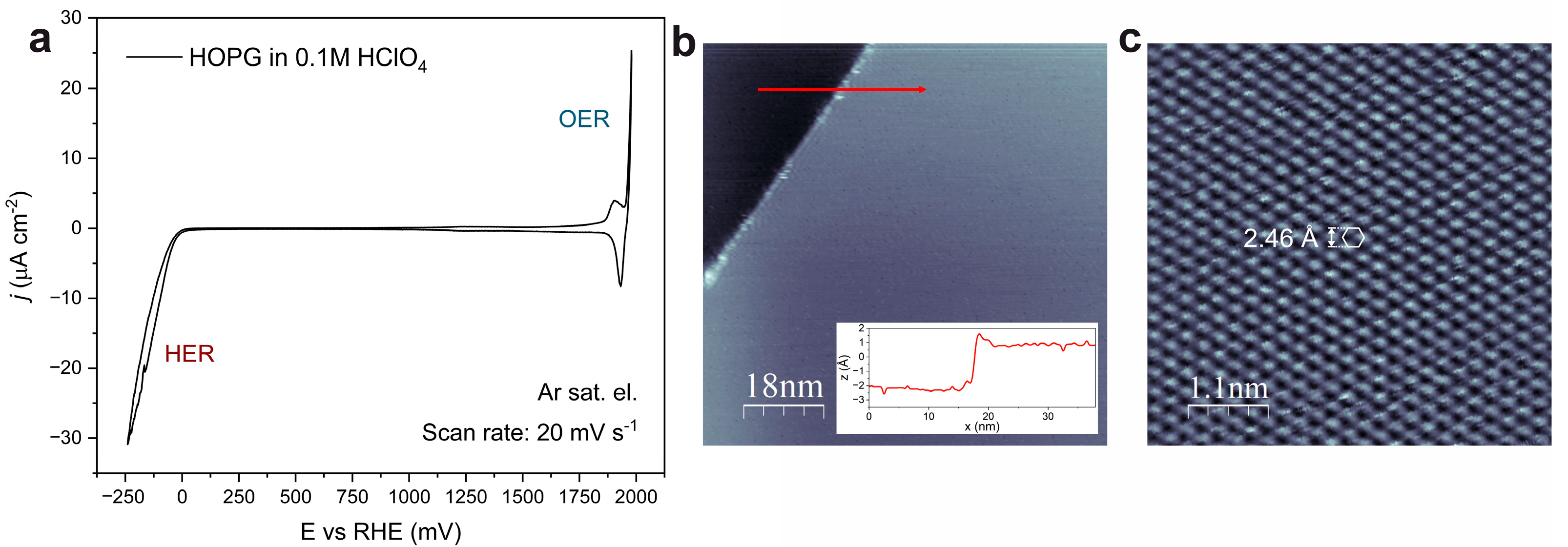
Figure 5 displays a typical CV curve recorded during these experiments, along with large-scale and high-resolution STM images. The CV curve reflects the expected electrochemical behavior of the HOPG surface, with the electrode potential window limited by the hydrogen evolution reaction (HER) on the cathodic side and perchlorate ion intercalation followed by the oxygen evolution reaction (OER) on the anodic side [57,58,59]. The large-scale STM image (Figure 5b), captured at an electrode potential of 270 mV, reveals terraces separated by monoatomic steps approximately 3.3 Å in height, consistent with the known interlayer spacing of graphite [60]. At atomic resolution, Figure 5c shows the hexagonal lattice structure of the HOPG surface, with a lattice spacing of approximately 2.46 Å. This spacing corresponds to the periodicity of every second carbon atom in the hexagonal lattice, a result of the ABAB stacking of graphene layers in HOPG [61].
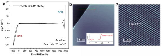
Figure 5.
(a) CV curve of a HOPG surface recorded in Ar-saturated 0.1 M HClO4 electrolyte. (b) Large-scale topography STM image of the HOPG surface, recorded at an electrode potential of 270 mV; inset shows the cross-section corresponding to the red line in (b). (c) High-resolution current STM image of the HOPG surface under the same conditions, demonstrating the tip’s ability to maintain precise imaging at the atomic scale. Tunneling conditions: (b) It = 1.6 nA, Ub = −235 mV; (c) It = 0.5 nA, Ub = −104 mV.
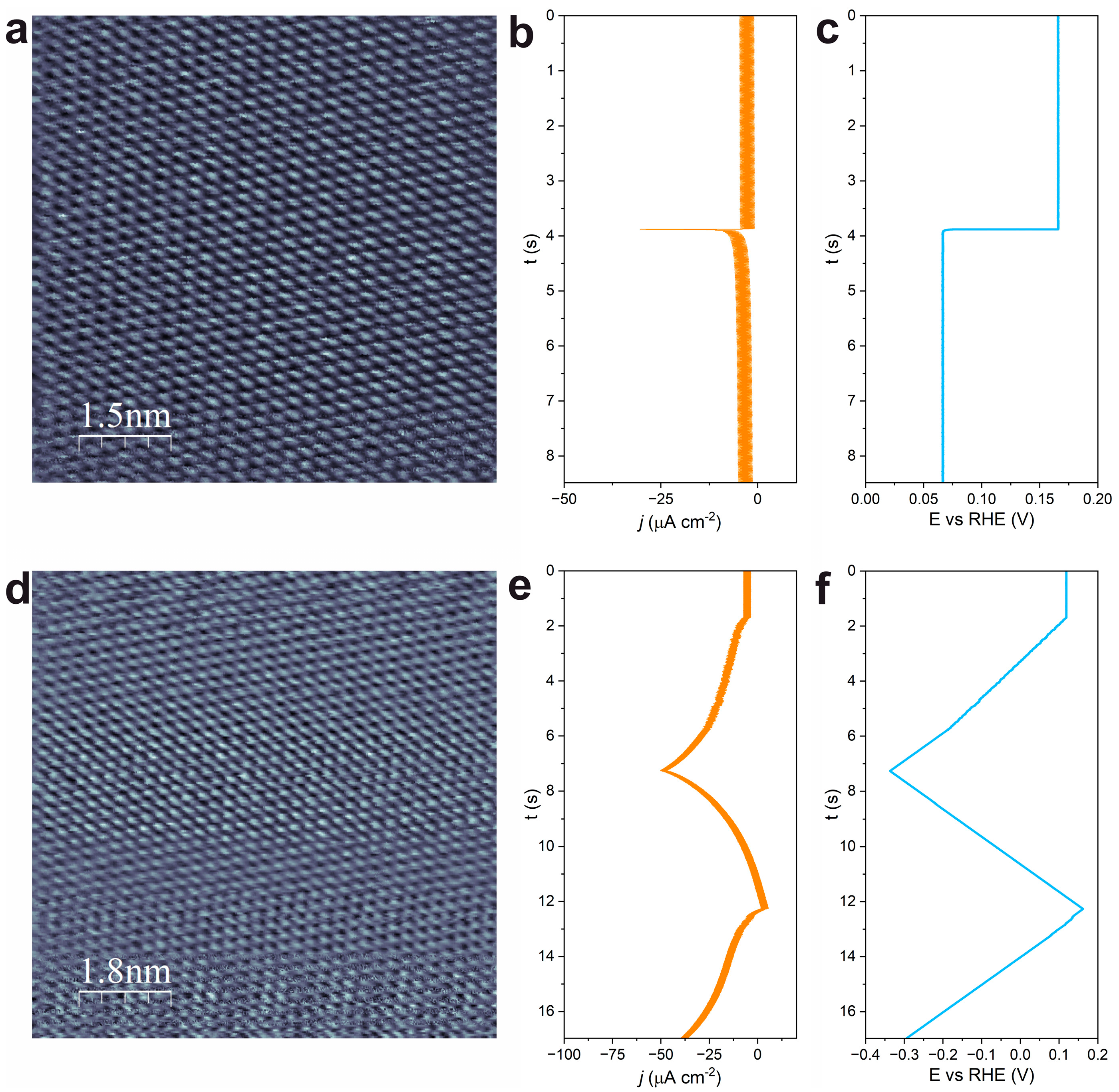
The ATC-coated tips were further subjected to rigorous testing under potentiodynamic conditions to evaluate their performance in maintaining atomic resolution during rapid and continuous changes in electrode potential. Figure 6 illustrates two critical scenarios where the electrode potential was dynamically varied while capturing STM images.
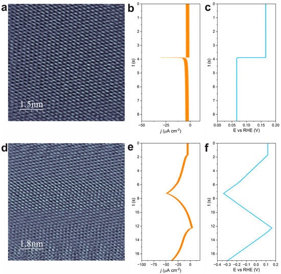
Figure 6.
Potentiodynamic STM imaging of the HOPG surface using an ATC-coated tip. (a) Atomic resolution STM image captured during rapid changes in electrode potential. (b) Corresponding current density vs. time plot, illustrating the current response to the dynamic potential changes. (c) Electrode potential vs. time plot, showing the timing of the rapid potential changes during the STM scan. (d) STM image of the HOPG surface obtained during continuous potentiodynamic imaging, with the electrode potential modulated at a rate of up to 100 mV/s, maintaining atomic resolution throughout. (e) Current density vs. time plot corresponding to the continuous potential modulation. (f) Electrode potential vs. time plot, demonstrating the continuous modulation of the electrode potential during imaging. Tunneling conditions: (a) It = 0.5 nA, Ub = −104 mV; (b) It = 1 nA, Ub = 234 mV.
In Figure 6a, an STM image of the HOPG surface with atomic resolution is shown. During the imaging process, the electrode potential was rapidly changed at a specific point, as indicated by the corresponding time-aligned plots in Figure 6b,c. The y-axis of the STM image in Figure 6a is directly correlated with the time axis in Figure 6b,c, providing a clear visualization of how the STM image changes as the electrode potential is abruptly altered. Despite the rapid potential change, the ATC-coated tip maintained its resolution, successfully capturing the atomic structure of the HOPG surface without any significant loss of imaging quality.
Figure 6d–f presents a second scenario where the electrode potential was continuously varied during the STM imaging process. In this experiment, the potential was systematically ramped up and down at a rate up to 100 mV/s, as shown in the corresponding plots. The y-axis in the STM image (Figure 6d) again corresponds to the time axis in the electrochemical data plots (Figure 6e,f). Even under these dynamically changing conditions, the ATC-coated tip consistently resolved the atomic lattice of the HOPG surface, demonstrating its robustness and stability under potentiodynamic conditions.
These results underscore the capability of the ATC-coated tips to operate reliably under challenging electrochemical environments. The ability to maintain atomic resolution during rapid and continuous changes in electrode potential is a crucial requirement for in situ and operando EC-STM studies, where capturing real-time structural dynamics at the atomic level is essential. The ATC’s consistent performance under these conditions validates its effectiveness in producing high-quality, insulated tips that can withstand the rigorous demands of advanced EC-STM research.
4. Conclusions
This study presents the development and application of an Automatic Tip Coater (ATC) designed to address the challenges of achieving high-quality, reproducible tip coatings for EC-STM. The ATC key features, including a precision tip movement system, a rotational module, and a temperature-controlled heating block, enable the consistent and uniform application of insulating materials, significantly reducing the variability often associated with manual coating methods.
The ATC-coated tips demonstrated a superior insulation performance, as evidenced by cyclic voltammetry (CV) tests conducted at a scan rate of 50 mV/s in a 0.1 M HClO4 electrolyte. The results showed that over 75% of the tips maintained leakage currents below 50 pA, with a substantial subset (30%) achieving currents as low as ±10 pA, indicating the high quality of the coatings. The ability to perform reliably at such a high scan rate is particularly noteworthy as it allows for the rapid screening and evaluation of multiple tips, an important factor in EC-STM research. In contrast, manually coated tips often struggle to achieve such a consistent performance due to issues with excess material and uneven coatings. This can result in significant variability in tip performance, leading to inconsistencies in data quality and reliability. By standardizing the coating process and reducing dependence on operator skills, the ATC ensures a consistent coating quality across batches, making the process more accessible to new users while significantly reducing the variability associated with manual methods.
Further validation under in situ and operando conditions using the HOPG surface confirmed the stability of the ATC-coated tips. The tips maintained an atomic resolution even under dynamic electrochemical conditions, demonstrating their robustness and reliability in capturing detailed surface phenomena.
In summary, the introduction of the ATC offers a reproducible solution for tip coating that enhances the accuracy and reliability of the EC-STM studies. By automating a process that traditionally relies heavily on operator skill, the ATC reduces experimental variability, lowers research costs, and contributes to the standardization of EC-STM methodologies. This innovation aids the exploration of surface phenomena at the atomic level, particularly in fields such as electrocatalysis, energy storage, and materials science, where precise and reliable measurements are paramount.
5. Patents
Patent application PL448634 has been submitted to the Polish Patent Office for the ATC described in this paper.
Supplementary Materials
The following supporting information can be downloaded at https://www.mdpi.com/article/10.3390/surfaces7040065/s1, Videos S1 and S2: Movies demonstrating the tip coating process. Figure S1 shows images of manual tip coater, and Figure S2 presents CV curves and statistical analysis of insulation performance for 74 manually coated tips.
Author Contributions
Conceptualization, R.K., P.W., T.K. and R.W.; methodology, R.K., P.W., A.F., T.K. and R.W.; software, R.K.; validation, P.W., A.F. and T.K.; formal analysis, R.K, P.W., A.F., T.K. and R.W.; investigation, R.K., P.W., A.F., T.K. and R.W.; resources, T.K. and R.W.; data curation, T.K.; writing—original draft preparation, T.K.; writing—review and editing, P.W., A.F., T.K. and R.W.; visualization, P.W., T.K. and R.W.; supervision, T.K. and R.W.; project administration, T.K. and R.W.; funding acquisition, T.K. All authors have read and agreed to the published version of the manuscript.
Funding
This research was funded by the National Science Center (Poland) under the SONATA 17 Project No. 2021/43/D/ST3/02873. For the purpose of Open Access, the author has applied a CC-BY public copyright license to any Author Accepted Manuscript (AAM) version arising from this submission.
Institutional Review Board Statement
Not applicable.
Informed Consent Statement
Not applicable.
Data Availability Statement
The data presented in this study are openly available in the OSF repository at DOI 10.17605/OSF.IO/K7A3N.
Conflicts of Interest
The authors declare no conflicts of interest.
References
- Nowicki, M.; Wandelt, K. Electrochemical Scanning Tunneling Microscopy. In Encyclopedia of Interfacial Chemistry: Surface Science and Electrochemistry; Elsevier: Amsterdam, The Netherlands, 2018; pp. 108–128. ISBN 9780128098943. [Google Scholar]
- Gentz, K.; Wandelt, K. Electrochemical Scanning Tunneling Microscopy. In Fundamentals of Picoscience; Sattler, K., Ed.; Taylor & Francis: Abingdon, UK, 2013; p. 269. ISBN 9781466505094. [Google Scholar]
- Yagati, A.K.; Min, J.; Choi, J.-W. Electrochemical Scanning Tunneling Microscopy (ECSTM)—From Theory to Future Applications. In Modern Electrochemical Methods in Nano, Surface and Corrosion Science; InTech: London, UK, 2014; ISBN 9789535157595. [Google Scholar]
- Facchin, A.; Kosmala, T.; Gennaro, A.; Durante, C. Electrochemical Scanning Tunneling Microscopy Investigations of FeN 4—Based Macrocyclic Molecules Adsorbed on Au(111) and Their Implications in the Oxygen Reduction Reaction. ChemElectroChem 2020, 7, 1431–1437. [Google Scholar] [CrossRef]
- Kosmala, T.; Calvillo, L.; Agnoli, S.; Granozzi, G. Enhancing the Oxygen Electroreduction Activity through Electron Tunnelling: CoOx Ultrathin Films on Pd(100). ACS Catal. 2018, 8, 2343–2352. [Google Scholar] [CrossRef]
- Kosmala, T.; Bibent, N.; Sougrati, M.T.; Dražić, G.; Agnoli, S.; Jaouen, F.; Granozzi, G. Stable, Active, and Methanol-Tolerant PGM-Free Surfaces in an Acidic Medium: Electron Tunneling at Play in Pt/FeNC Hybrid Catalysts for Direct Methanol Fuel Cell Cathodes. ACS Catal. 2020, 10, 7475–7485. [Google Scholar] [CrossRef]
- Ye, C.Q.; Hu, R.G.; Li, Y.; Lin, C.J.; Pan, J.S. Probing the Vertical Profiles of Potential in a Thin Layer of Solution Closed to Electrode Surface during Localized Corrosion of Stainless Steel. Corros. Sci. 2012, 61, 242–245. [Google Scholar] [CrossRef]
- Marcus, P. Surface Science Approach of Corrosion Phenomena. Electrochim. Acta 1998, 43, 109–118. [Google Scholar] [CrossRef]
- Zhu, L.; Hommet, F.; Salace, G.; Claude-Montigny, B.; Métrot, A. STM Observation of the Electro-Adsorption of Lithium Ions onto Graphite and of the Ensuing Solid Electrolyte Interphase Formation. Surf. Sci. 2002, 512, 84–96. [Google Scholar] [CrossRef]
- Wang, L.; Deng, X.; Dai, P.X.; Guo, Y.G.; Wang, D.; Wan, L.J. Initial Solid Electrolyte Interphase Formation Process of Graphite Anode in LiPF 6 Electrolyte: An in Situ ECSTM Investigation. Phys. Chem. Chem. Phys. 2012, 14, 7330–7336. [Google Scholar] [CrossRef]
- Kolb, D.M.; Ullmann, R.; Will, T. Nanofabrication of Small Copper Clusters on Gold(111) Electrodes by a Scanning Tunneling Microscope. Science 1997, 275, 1097–1099. [Google Scholar] [CrossRef]
- Alessandrini, A.; Facci, P. Electron Transfer in Nanobiodevices. Eur. Polym. J. 2016, 83, 450–466. [Google Scholar] [CrossRef]
- Kosmala, T.; Agnoli, S.; Granozzi, G. Watching Atoms at Work during Reactions. Pure Appl. Chem. 2024, 96, 457–463. [Google Scholar] [CrossRef]
- Feng, H.; Xu, X.; Du, Y.; Dou, S.X. Application of Scanning Tunneling Microscopy in Electrocatalysis and Electrochemistry. Electrochem. Energy Rev. 2021, 4, 249–268. [Google Scholar] [CrossRef]
- Kosmala, T.; Baby, A.; Lunardon, M.; Perilli, D.; Liu, H.; Durante, C.; Di Valentin, C.; Agnoli, S.; Granozzi, G. Operando Visualization of the Hydrogen Evolution Reaction with Atomic-Scale Precision at Different Metal–Graphene Interfaces. Nat. Catal. 2021, 4, 850–859. [Google Scholar] [CrossRef]
- Lunardon, M.; Kosmala, T.; Ghorbani-Asl, M.; Krasheninnikov, A.V.; Kolekar, S.; Durante, C.; Batzill, M.; Agnoli, S.; Granozzi, G. Catalytic Activity of Defect-Engineered Transition Me Tal Dichalcogenides Mapped with Atomic-Scale Precision by Electrochemical Scanning Tunneling Microscopy. ACS Energy Lett. 2023, 8, 972–980. [Google Scholar] [CrossRef] [PubMed]
- Lunardon, M.; Kosmala, T.; Durante, C.; Agnoli, S.; Granozzi, G. Atom-by-Atom Identification of Catalytic Active Sites in Operando Conditions by Quantitative Noise Detection. Joule 2022, 6, 617–635. [Google Scholar] [CrossRef]
- Liang, Y.; Csoklich, C.; McLaughlin, D.; Schneider, O.; Bandarenka, A.S. Revealing Active Sites for Hydrogen Evolution at Pt and Pd Atomic Layers on Au Surfaces. ACS Appl. Mater. Interfaces 2019, 11, 12476–12480. [Google Scholar] [CrossRef]
- Pfisterer, J.H.K.; Liang, Y.; Schneider, O.; Bandarenka, A.S. Direct Instrumental Identification of Catalytically Active Surface Sites. Nature 2017, 549, 74–77. [Google Scholar] [CrossRef]
- Mitterreiter, E.; Liang, Y.; Golibrzuch, M.; Mclaughlin, D.; Csoklich, C.; Bartl, J.D.; Holleitner, A.; Wurstbauer, U.; Bandarenka, A.S. In-Situ Visualization of Hydrogen Evolution Sites on Helium Ion Treated Molybdenum Dichalcogenides under Reaction Conditions. NPJ 2D Mater. Appl. 2019, 3, 25. [Google Scholar] [CrossRef]
- Haid, R.W.; Kluge, R.M.; Liang, Y.; Bandarenka, A.S. In Situ Quantification of the Local Electrocatalytic Activity via Electrochemical Scanning Tunneling Microscopy. Small Methods 2021, 5, 2000710. [Google Scholar] [CrossRef]
- Schmidt, T.O.; Haid, R.W.; Gubanova, E.L.; Kluge, R.M.; Bandarenka, A.S. Electrochemical Scanning Tunneling Microscopy as a Tool for the Detection of Active Electrocatalytic Sites. Topics in Catalysis 2023, 66, 1270–1279. [Google Scholar] [CrossRef]
- Liang, Y.; McLaughlin, D.; Csoklich, C.; Schneider, O.; Bandarenka, A.S. The Nature of Active Centers Catalyzing Oxygen Electro-Reduction at Platinum Surfaces in Alkaline Media. Energy Environ. Sci. 2019, 12, 351–357. [Google Scholar] [CrossRef]
- Haid, R.W.; Kluge, R.M.; Schmidt, T.O.; Bandarenka, A.S. In-Situ Detection of Active Sites for Carbon-Based Bifunctional Oxygen Reduction and Evolution Catalysis. Electrochim. Acta 2021, 382, 138285. [Google Scholar] [CrossRef]
- Kluge, R.M.; Haid, R.W.; Bandarenka, A.S. Assessment of Active Areas for the Oxygen Evolution Reaction on an Amorphous Iridium Oxide Surface. J. Catal. 2021, 396, 14–22. [Google Scholar] [CrossRef]
- Kluge, R.M.; Haid, R.W.; Stephens, I.E.L.; Calle-Vallejo, F.; Bandarenka, A.S. Monitoring the Active Sites for the Hydrogen Evolution Reaction at Model Carbon Surfaces. Phys. Chem. Chem. Phys. 2021, 23, 10051–10058. [Google Scholar] [CrossRef]
- Bach, C.E.; Nichols, R.J.; Beckmann, W.; Meyer, H.; Schulte, A.; Besenhard, J.O.; Jannakoudakis, P.D. Effective Insulation of Scanning Tunneling Microscopy Tips for Electrochemical Studies Using an Electropainting Method. J. Electrochem. Soc. 1993, 140, 1281–1284. [Google Scholar] [CrossRef]
- Itaya, K.; Tomita, E. Scanning Tunneling Microscope for Electrochemistry—A New Concept for the in Situ Scanning Tunneling Microscope in Electrolyte Solutions. Surf. Sci. 1988, 201, L507–L512. [Google Scholar] [CrossRef]
- Heben, M.J.; Dovek, M.M.; Lewis, N.S.; Penner, R.M.; Quate, C.F. Preparation of STM Tips for In-situ Characterization of Electrode Surfaces. J. Microsc. 1988, 152, 651–661. [Google Scholar] [CrossRef]
- Penner, R.M.; Heben, M.J.; Lewis, N.S. Preparation and Electrochemical Characterization of Conical and Hemispherical Ultramicroelectrodes. Anal. Chem. 1989, 61, 1630–1636. [Google Scholar] [CrossRef]
- Kobayashi, Y.; Yokota, Y.; Takahashi, Y.; Takeya, J.; Kim, Y. Electrodeposited Gold Probe for Electrochemical Scanning Tunneling Microscopy. J. Phys. Chem. C 2023, 127, 13929–13935. [Google Scholar] [CrossRef]
- Schneir, J.; Hansma, P.K.; Elings, V.; Gurley, J.; Wickramasinghe, K.; Sonnenfeld, R. Creating and Observing Surface Features with A Scanning Tunneling Microscope. In Scanning Microscopy Technologies and Applications; SPIE: Bellingham, WA, USA, 1988; Volume 897, pp. 16–21. [Google Scholar]
- Abelev, E.; Sezin, N.; Ein-Eli, Y. An Alternative Isolation of Tungsten Tips for a Scanning Tunneling Microscope. Rev. Sci. Instrum. 2005, 76, 106105. [Google Scholar] [CrossRef]
- Zhu, L.; Claude-Montigny, B.; Gattrell, M. Insulating Method Using Cataphoretic Paint for Tungsten Tips for Electrochemical Scanning Tunnelling Microscopy (ECSTM). Appl. Surf. Sci. 2005, 252, 1833–1845. [Google Scholar] [CrossRef]
- Salerno, M. Coating of Tips for Electrochemical Scanning Tunneling Microscopy by Means of Silicon, Magnesium, and Tungsten Oxides. Rev. Sci. Instrum. 2010, 81, 093703. [Google Scholar] [CrossRef] [PubMed]
- Hacker, B.; Hillebrand, A.; Hartmann, T.; Guckenberger, R. Preparation and Characterization of Tips for Scanning Tunneling Microscopy of Biological Specimens. Ultramicroscopy 1992, 42–44, 1514–1518. [Google Scholar] [CrossRef]
- Zhang, B.; Wang, E. Fabrication of STM Tips with Controlled Geometry by Electrochemical Etching and ECSTM Tips Coated with Paraffin. Electrochim. Acta 1994, 39, 103–106. [Google Scholar] [CrossRef]
- Green, M.P.; Hanson, K.J.; Scherson, D.A.; Xing, X.; Richter, M.; Ross, P.N.; Carr, R.; Lindau, I. In Situ Scanning Tunneling Microscopy Studies of the Underpotential Deposition of Lead on Gold (111). J. Phys. Chem. 1989, 93, 2181–2184. [Google Scholar] [CrossRef]
- Vitus, C.M.; Chang, S.C.; Schardt, B.C.; Weaver, M.J. In Situ Scanning Tunneling Microscopy as a Probe of Adsorbate-Induced Reconstruction at Ordered Monocrystalline Electrodes: Carbon Monoxide on Platinum(100). J. Phys. Chem. 1991, 95, 7559–7563. [Google Scholar] [CrossRef]
- Gewirth, A.A.; Craston, D.H.; Bard, A.J. Fabrication and Characterization of Microtips for in Situ Scanning Tunneling Microscopy. J. Electroanal. Chem. Interfacial Electrochem. 1989, 261, 477–482. [Google Scholar] [CrossRef]
- Chen, Z.F.; Wang, E. Fabrication and Characterization of Tips for Electrochemical Scanning Tunneling Microscopy. Electroanalysis 1994, 6, 672–676. [Google Scholar] [CrossRef]
- Breuer, N.; Stimming, U.; Vogel, R. An Investigation of the Temporal Dynamics of Metal Cluster on Electrode Surfaces. Surf. Coat. Technol. 1994, 67, 145–149. [Google Scholar] [CrossRef]
- Silva, E.L.; Neto, M.A.; Fernandes, A.J.S.; Bastos, A.C.; Silva, R.F.; Zheludkevich, M.L.; Oliveira, F.J. Fast Coating of Ultramicroelectrodes with Boron-Doped Nanocrystalline Diamond. Diam. Relat. Mater. 2010, 19, 1330–1335. [Google Scholar] [CrossRef]
- Wang, E. Electrochemical Scanning Tunneling Microscopy. Anal. Sci. 1994, 10, 155–156. [Google Scholar] [CrossRef]
- Phan, T.H.; Kosmala, T.; Wandelt, K. Potential Dependence of Self-Assembled Porphyrin Layers on a Cu(111) Electrode Surface: In-Situ STM Study. Surf. Sci. 2015, 631, 207–212. [Google Scholar] [CrossRef]
- Phan, T.; Wandelt, K. Molecular Self-Assembly at Metal-Electrolyte Interfaces. Int. J. Mol. Sci. 2013, 14, 4498–4524. [Google Scholar] [CrossRef] [PubMed]
- Wiechers, J.; Twomey, T.; Kolb, D.M.; Behm, R.J. An In-Situ Scanning Tunneling Microscopy Study of Au (111) with Atomic Scale Resolution. J. Electroanal. Chem. Interfacial Electrochem. 1988, 248, 451–460. [Google Scholar] [CrossRef]
- Nagahara, L.A.; Thundat, T.; Lindsay, S.M. Preparation and Characterization of STM Tips for Electrochemical Studies. Rev. Sci. Instrum. 1989, 60, 3128–3130. [Google Scholar] [CrossRef]
- Kobayashi, Y.; Yokota, Y.; Wong, R.A.; Hong, M.; Takeya, J.; Osawa, S.; Ishiwari, F.; Shoji, Y.; Harimoto, T.; Sugimoto, K.; et al. Single-Molecule Observation of Redox Reactions Enabled by Rigid and Isolated Tripodal Molecules. J. Phys. Chem. C 2023, 127, 746–758. [Google Scholar] [CrossRef]
- Kazinczi, R.; Szõcs, E.; Kálmán, E.; Nagy, P. Novel Methods for Preparing EC STM Tips. Appl. Phys. A Mater. Sci. Process. 1998, 66, S535–S538. [Google Scholar] [CrossRef]
- Hugelmann, P.; Schindler, W. In-Situ Voltage Tunneling Spectroscopy at Electrochemical Interfaces. J. Phys. Chem. B 2005, 109, 6262–6267. [Google Scholar] [CrossRef]
- Holland, I.; Davies, J.A. Automation in the Life Science Research Laboratory. Front. Bioeng. Biotechnol. 2020, 8, 571777. [Google Scholar] [CrossRef] [PubMed]
- Kosmala, T.; Wasielewski, R.; Nowicki, M.; Wandelt, K. Unveiling the Interplay between a Au(100) Electrode, Adsorbed TTMAPP Porphyrin Cations, and Iodide Anions: An EC-STM and CV Study. J. Phys. Chem. C 2024, 128, 1773–1789. [Google Scholar] [CrossRef]
- Madry, B.; Morawski, I.; Kosmala, T.; Wandelt, K.; Nowicki, M. Porphyrin Layers at Cu/Au(111)–Electrolyte Interfaces: In Situ EC-STM Study. Top. Catal. 2018, 61, 1335–1349. [Google Scholar] [CrossRef]
- Matsubara, Y. A Small yet Complete Framework for a Potentiostat, Galvanostat, and Electrochemical Impedance Spectrometer. J. Chem. Educ. 2021, 98, 3362–3370. [Google Scholar] [CrossRef]
- Wilms, M.; Kruft, M.; Bermes, G.; Wandelt, K. A New and Sophisticated Electrochemical Scanning Tunneling Microscope Design for the Investigation of Potentiodynamic Processes. Rev. Sci. Instrum. 1999, 70, 3641. [Google Scholar] [CrossRef]
- Bussetti, G.; Yivlialin, R.; Alliata, D.; Li Bassi, A.; Castiglioni, C.; Tommasini, M.; Casari, C.S.; Passoni, M.; Biagioni, P.; Ciccacci, F.; et al. Disclosing the Early Stages of Electrochemical Anion Intercalation in Graphite by a Combined Atomic Force Microscopy/Scanning Tunneling Microscopy Approach. J. Phys. Chem. C 2016, 120, 6088–6093. [Google Scholar] [CrossRef]
- Schnyder, B.; Alliata, D.; Kötz, R.; Siegenthaler, H. Electrochemical Intercalation of Perchlorate Ions in HOPG: An SFM/LFM and XPS Study. Appl. Surf. Sci. 2001, 173, 221–232. [Google Scholar] [CrossRef]
- Yivlialin, R.; Bussetti, G.; Brambilla, L.; Castiglioni, C.; Tommasini, M.; Duò, L.; Passoni, M.; Ghidelli, M.; Casari, C.S.; Li Bassi, A. Microscopic Analysis of the Different Perchlorate Anions Intercalation Stages of Graphite. J. Phys. Chem. C 2017, 121, 14246–14253. [Google Scholar] [CrossRef]
- Xu, R.; Yin, L.-J.; Qiao, J.-B.; Bai, K.-K.; Nie, J.-C.; He, L. Direct Probing of the Stacking Order and Electronic Spectrum of Rhombohedral Trilayer Graphene with Scanning Tunneling Microscopy. Phys. Rev. B 2015, 91, 035410. [Google Scholar] [CrossRef]
- Tománek, D.; Louie, S.G.; Mamin, H.J.; Abraham, D.W.; Thomson, R.E.; Ganz, E.; Clarke, J. Theory and Observation of Highly Asymmetric Atomic Structure in Scanning-Tunneling-Microscopy Images of Graphite. Phys. Rev. B 1987, 35, 7790–7793. [Google Scholar] [CrossRef]
Disclaimer/Publisher’s Note: The statements, opinions and data contained in all publications are solely those of the individual author(s) and contributor(s) and not of MDPI and/or the editor(s). MDPI and/or the editor(s) disclaim responsibility for any injury to people or property resulting from any ideas, methods, instructions or products referred to in the content. |
© 2024 by the authors. Licensee MDPI, Basel, Switzerland. This article is an open access article distributed under the terms and conditions of the Creative Commons Attribution (CC BY) license (https://creativecommons.org/licenses/by/4.0/).

