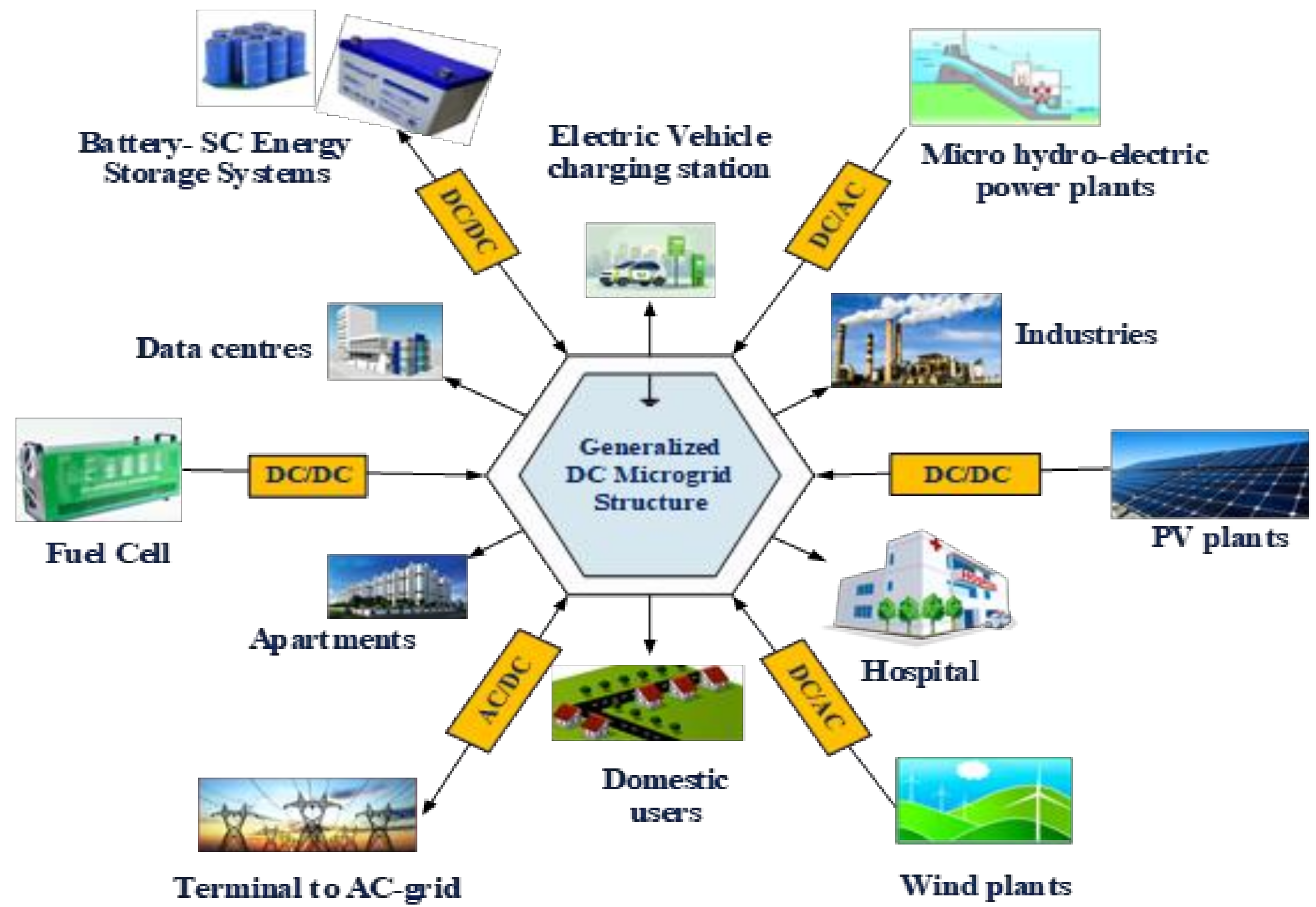
Figure 1.
DC microgrid architecture.
Figure 1.
DC microgrid architecture.
Figure 2.
HESS and PV system in a DC microgrid design.
Figure 2.
HESS and PV system in a DC microgrid design.
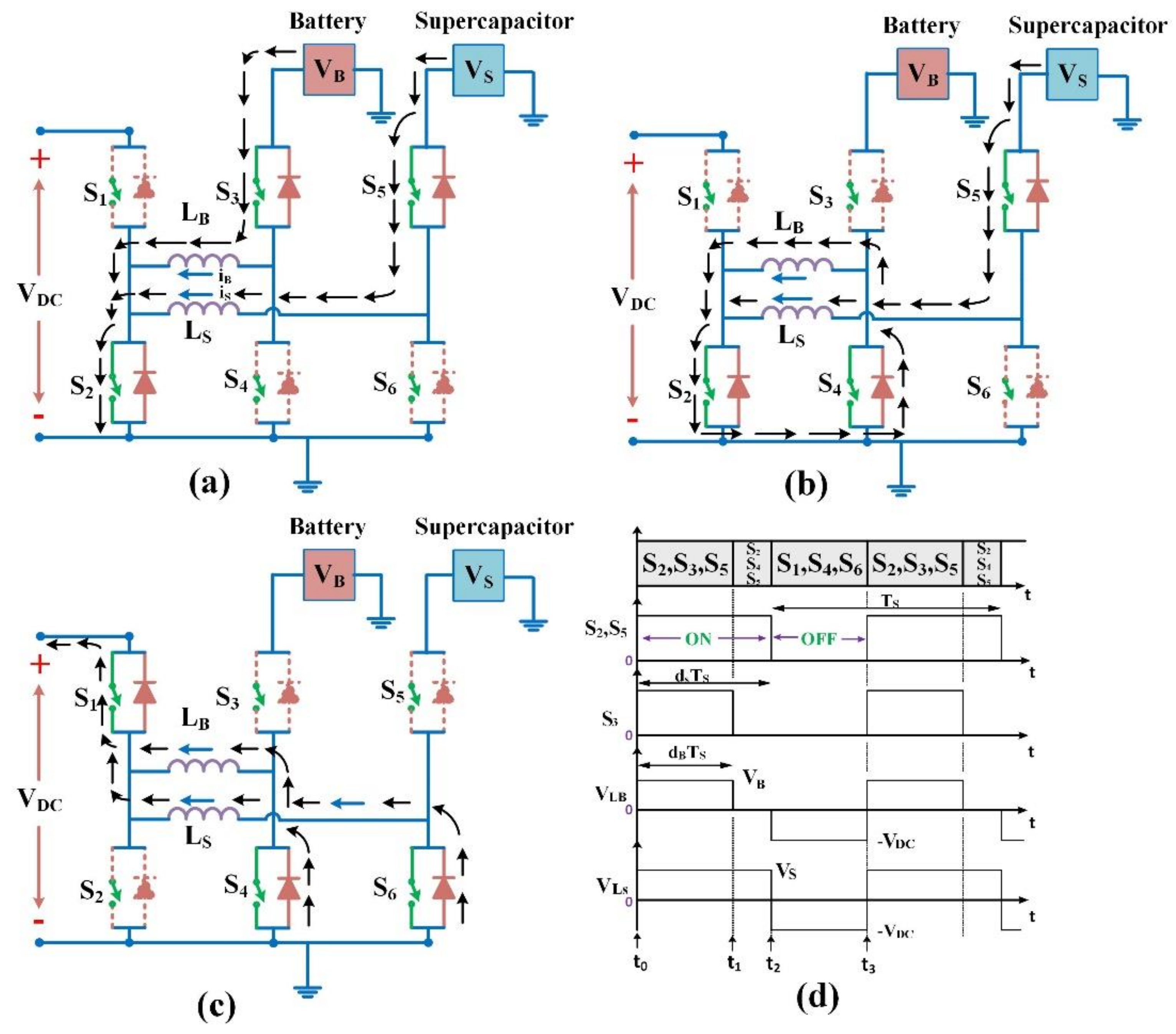
Figure 3.
Two-input bidirectional converter equivalent circuit. (a) Operating switches S2, S3 and S5; (b) operating switches S2, S4 and S5; (c) operating switches S1, S4 and S6 and (d) discharging mode steady-state waveforms.
Figure 3.
Two-input bidirectional converter equivalent circuit. (a) Operating switches S2, S3 and S5; (b) operating switches S2, S4 and S5; (c) operating switches S1, S4 and S6 and (d) discharging mode steady-state waveforms.
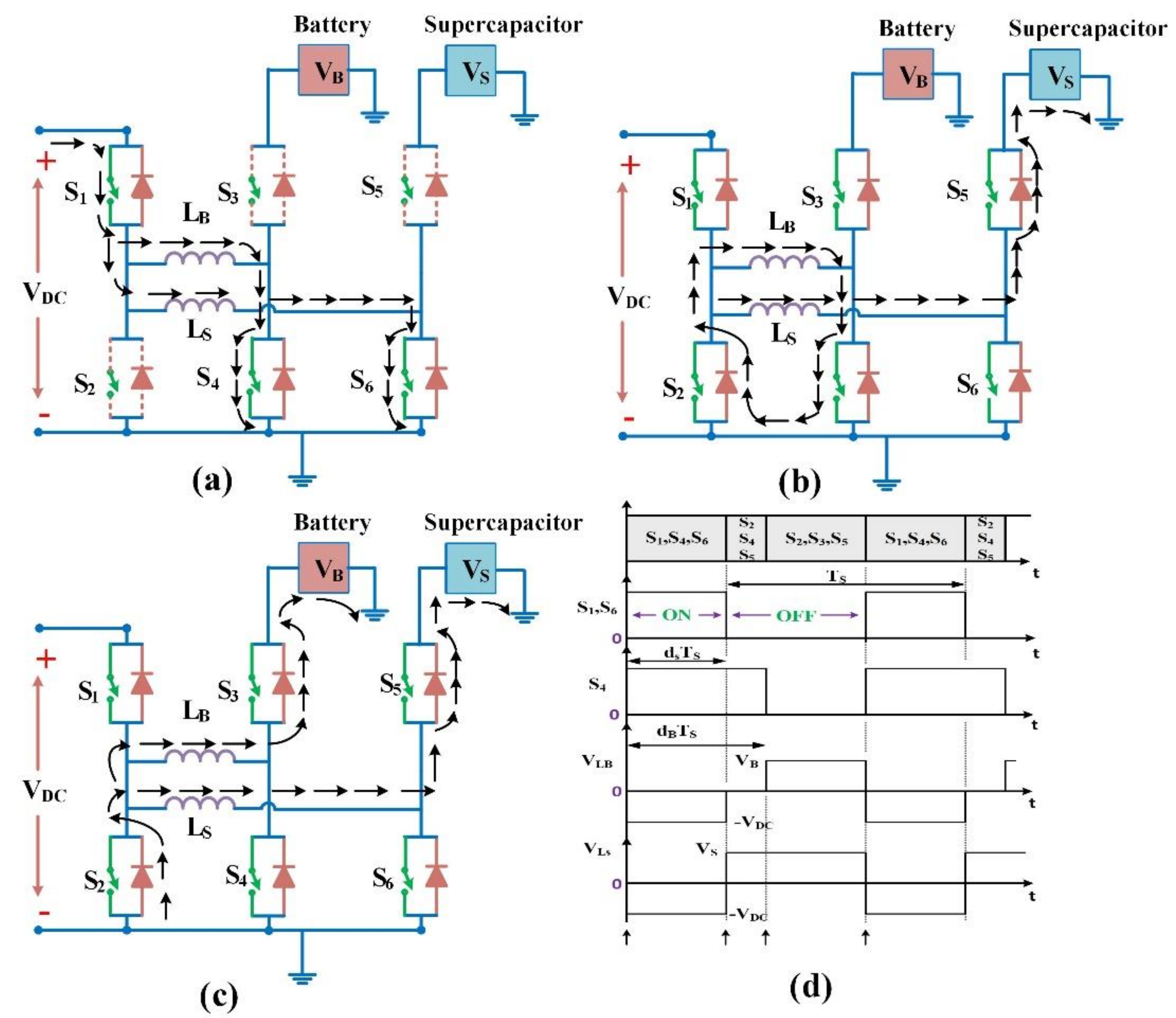
Figure 4.
Two-input bi-directional converter equivalent circuit. (a) Operating switchesS1, S4 and S6; (b) operating switches S2, S4 and S5; (c) operating switches S2, S3 and S5 and (d) steady-state waveforms in discharging mode.
Figure 4.
Two-input bi-directional converter equivalent circuit. (a) Operating switchesS1, S4 and S6; (b) operating switches S2, S4 and S5; (c) operating switches S2, S3 and S5 and (d) steady-state waveforms in discharging mode.
Figure 5.
HESS energy exchange method of operation: (a) equivalent circuit and (b) steady-state waveforms.
Figure 5.
HESS energy exchange method of operation: (a) equivalent circuit and (b) steady-state waveforms.
Figure 6.
Description of the overall control mechanism for the current bifurcation between the SC and the battery unit for the PI control scheme.
Figure 6.
Description of the overall control mechanism for the current bifurcation between the SC and the battery unit for the PI control scheme.
Figure 7.
Overall block diagram: (a) representation of supercapacitor control logic and (b) representation of battery control logic.
Figure 7.
Overall block diagram: (a) representation of supercapacitor control logic and (b) representation of battery control logic.
Figure 8.
With and without compensation, a Bode plot of the inner SC current logic.
Figure 8.
With and without compensation, a Bode plot of the inner SC current logic.
Figure 9.
With and without correction, an open-loop Bode plot of battery current logic is shown.
Figure 9.
With and without correction, an open-loop Bode plot of battery current logic is shown.
Figure 10.
Bode diagram of the outer voltage logic in open loop with and without compensation.
Figure 10.
Bode diagram of the outer voltage logic in open loop with and without compensation.
Figure 11.
Block diagram representation of MPC for HESS.
Figure 11.
Block diagram representation of MPC for HESS.
Figure 12.
Change in PV generation using a PI control system simulation. (a) PV power, (b) output load power, (c) battery storage power, (d) SC storage power, (e) PV current, (f) DC microgrid voltage, (g) battery storage current and (h) SC storage current.
Figure 12.
Change in PV generation using a PI control system simulation. (a) PV power, (b) output load power, (c) battery storage power, (d) SC storage power, (e) PV current, (f) DC microgrid voltage, (g) battery storage current and (h) SC storage current.
Figure 13.
The simulation findings for a change in load demand are as follows: (a) DC microgrid power, (b) battery storage power, (c) SC storage power, (d) SC SOC, (e) DC microgrid voltage, (f) DC microgrid current, (g) battery storage current and (h) SC storage current.
Figure 13.
The simulation findings for a change in load demand are as follows: (a) DC microgrid power, (b) battery storage power, (c) SC storage power, (d) SC SOC, (e) DC microgrid voltage, (f) DC microgrid current, (g) battery storage current and (h) SC storage current.
Figure 14.
Simulation findings for MPC control of a step change in PV generation (a) PV power generation, (b) load power demand, (c) battery storage power, (d) SC storage power, (e) PV current generation, (f) DC microgrid voltage, (g) battery storage current and (h) SC storage current.
Figure 14.
Simulation findings for MPC control of a step change in PV generation (a) PV power generation, (b) load power demand, (c) battery storage power, (d) SC storage power, (e) PV current generation, (f) DC microgrid voltage, (g) battery storage current and (h) SC storage current.
Figure 15.
Simulation results for a load demand step change—(a) DC microgrid power demand, (b) battery storage power, (c) SC storage power, (d) SC SOC, (e) DC microgrid voltage, (f) DC grid current, (g) battery storage current and (h) SC current.
Figure 15.
Simulation results for a load demand step change—(a) DC microgrid power demand, (b) battery storage power, (c) SC storage power, (d) SC SOC, (e) DC microgrid voltage, (f) DC grid current, (g) battery storage current and (h) SC current.
Figure 16.
Graphical comparison of PI controller performance over MPC: (a) settling time and (b) peak overshoot.
Figure 16.
Graphical comparison of PI controller performance over MPC: (a) settling time and (b) peak overshoot.
Figure 17.
Comparative performance of PI controller over MPC: (a) step change in PV, (b) battery current, (c) step change in load demand and (d) SC current.
Figure 17.
Comparative performance of PI controller over MPC: (a) step change in PV, (b) battery current, (c) step change in load demand and (d) SC current.
Figure 18.
Hardware prototype developed for HESS.
Figure 18.
Hardware prototype developed for HESS.
Figure 19.
Experiments on a step change in PV production have yielded promising results. (a) Step increase in PV generation, (b) step decrease in PV generation and (c) step increase and decrease in PV generation.
Figure 19.
Experiments on a step change in PV production have yielded promising results. (a) Step increase in PV generation, (b) step decrease in PV generation and (c) step increase and decrease in PV generation.
Figure 20.
Experiments on a step change in load demand yielded the following findings: (a) step increase in load demand, (b) step decrease in load demand and (c) step increase and decrease in load demand.
Figure 20.
Experiments on a step change in load demand yielded the following findings: (a) step increase in load demand, (b) step decrease in load demand and (c) step increase and decrease in load demand.
Table 1.
Switching operation in various time intervals.
Table 1.
Switching operation in various time intervals.
| Time Scale | T1 | T2 | T3 |
|---|
| Operating switches | (S2–S3–S5) | (S2–S4–S5) | (S1–S4–S6) |
Table 2.
Changing states at various periods of time.
Table 2.
Changing states at various periods of time.
| Time Scale | T1 | T2 | T3 |
|---|
| Operating switches | (S1–S4–S6) | (S2–S4–S5) | (S2–S3–S5) |
Table 3.
Relationship between different voltages.
Table 3.
Relationship between different voltages.
| S. No | Mode of Operation | Transfer Function |
|---|
| 1 | Power transfer from Battery–SC bank to the DC grid | |
| 2 | Power transfer from DC grid to Battery–SC | |
| 3 | Energy exchange mode | |
Table 4.
Linear averaged transfer functions for small signals.
Table 4.
Linear averaged transfer functions for small signals.
| S. No. | Parameter | Transfer Functions |
|---|
| 1 | SC current transfer function control | |
| 2 | SC current to transfer function output voltage | |
| 3 | Control to battery current transfer function | |
| 4 | Inner SC current loop PI controller transfer function | |
| 5 | The transfer function of the battery current loop was controlled by a PI controller. | |
| 6 | Outer voltage control loop PI controller transfer function | |
Table 5.
Simulation study system parameters.
Table 5.
Simulation study system parameters.
| S. No | Parameters | Value |
|---|
| 1 | MPPT voltage (Vmppt) | 31.95 V |
| 2 | MPPT current (Imppt) | 3.05 A |
| 3 | MPPT power (Pmppt) | 96.05 W |
| 4 | SC voltage (VSC) | 32 V |
| 5 | SC storage inductance (LS) | 0.365 mH |
| 6 | Battery voltage (VB) | 24 V |
| 7 | Battery storage inductance (LB) | 0.35 mH |
| 8 | Boost converter inductance (L) | 4.2 mH |
| 9 | Load resistance (R) | 24 Ω |
| 10 | DC grid voltage (VDC) | 48 V |
| 11 | Output capacitance (C) | 400 µF |
Table 6.
Parameters for implementing a DC microgrid.
Table 6.
Parameters for implementing a DC microgrid.
| S. No | Parameters | Value |
|---|
| 1 | SC component voltage (VSC) | 10 V |
| 2 | SC component inductance (LS) | 1.43 mH |
| 3 | Battery component voltage (VB) | 12 V |
| 4 | Battery inductance (LB) | 4.8 mH |
| 5 | Boost converter inductance (L) | 4.1 mH |
| 6 | Load resistance (R) | 25 Ω |
| 7 | DC microgrid voltage (VDC) | 20 V |
| 8 | Filter capacitance (C) | 150 µF |


