1. Introduction
Bioelectronic devices serve as a platform to transfer biochemical information as electronic readout signals, the development of which provides ease of access to the chemical and biological world. Amperometric, potentiometric, and conductometric measurement methods are utilized among the variety of bioelectronic devices used as biosensors to study biophysical and biochemical events. Deploying light within such electrochemical systems, including light-addressable and light-readable systems, enables spatially-defined biochemical detection as well as manipulation. In this review article, we focus primarily on the recent developments of two major types of electrochemistry with meaningful light interactions - the photoelectronic effect within semiconductor materials, and electrogenerated chemiluminescence. We will also introduce promising multiplexed and imaging applications used to reveal detailed biochemistry with high spatial and temporal resolutions.
2. Light-Addressable Electrochemistry
Localized electrochemical information has conventionally been only available via discrete conductive electrodes based on metallic or carbon materials [
1,
2]. Taking advantage of the photoelectric effect within a semiconductor enables a shift of the electrochemical paradigm from individually connected measurement electrodes to the illumination of a focused light beam to enable photoelectrochemical sensing at specific locations. For example, photostimulus-enabled direct charge transfer at the electrolyte-semiconductor interface has gained tremendous popularity due to its unique light-addressability in defining measurement or manipulation spots [
3,
4].
Furthermore, an alternative structure is to add an insulating layer between the electrolyte and semiconductor to form an electrolyte-insulator-semiconductor (EIS) structure. Such an EIS structure blocks direct current flow and enables a new sensing mechanism based on the change in the space charge region at the semiconductor-insulator interface induced by the surface potential change at the semiconductor-electrolyte interface. The change in the space charge region can be read out in the form of an alternating photocurrent upon illumination via a modulated light beam [
5]. In this section, we will discuss light-addressable electrochemistry based on the two aforementioned mechanisms, i.e., the light-addressable potentiometric sensor (LAPS) and light-addressable electrode (LAE).
2.1. Light-Addressable Potentiometric Sensors (LAPS)
2.1.1. Background
Since the introduction of the ion sensitive field effect transistor (ISFET) by Bergveld et al. in 1970 [
6], researchers first derived the EIS capacitance from an early investigation on ISFETs to study the complex electrochemical and surface mechanisms of the ISFET-gate region [
7]. This was similar to the traditional development of the metal-oxide semiconductor field-effect transistor (MOSFET) and metal-oxide semiconductor (MOS) capacitances. EIS structures started to gain in popularity to serve as individual sensor platforms because of their relatively simple fabrication and encapsulation processes.
Traditional capacitance vs. voltage (C-V) measurements were mainly used to characterize the capacitance of the MOS and EIS structures. In addition, the scanned light pulse technique (SLPT) was introduced by Engström and Alm in 1983 [
8]. A light probe was used to address a local area of a MOS structure and a local photocurrent could be detected that was dependent on the local surface potential states of the illuminated region of the MOS structure. In 1988, a light-addressable potentiometric sensor was developed by a combination of this SLPT method with the EIS structure by Hafeman et al. [
9].
The surface potential of the electrolyte-transducer interface could be measured by such a sensor via the change in photocurrent at discrete locations. Hence, chemical interactions that induce surface potential changes could also be detected discretely using a LAPS. Ever since the development of the LAPS with its unique addressable features enabled by light, the LAPS has gained significant popularity on the historical stage, compared with its predecessors, for the following reasons:
Multiplexing different light sources at different locations equips the sensor with imaging ability and also the ability of multidetection for different biochemical events that occur on the LAPS [
10,
11].
The front surface of the LAPS is flat and smooth, which simplifies the surface modification process. For example, certain species, such as K
, Na
, and Ca
, can be detected by the deposition of ion-sensitive membranes on the LAPS surface [
12,
13].
The structure and fabrication process is simple.
Encapsulation is easier and less critical than for other devices because there is only one lead to the backside of the semiconductor and one or two electrode contacts to the electrolyte even when multiple sensing spots are used.
2.1.2. Working Principles of the LAPS
The LAPS is a semiconductor-based biochemical sensor that is sensitive to surface-potential changes. With an EIS structure, the concentration of biochemical species in a sample solution contacting the sensor surface can be detected, such as hydrogen ions on a silicon-nitride surface [
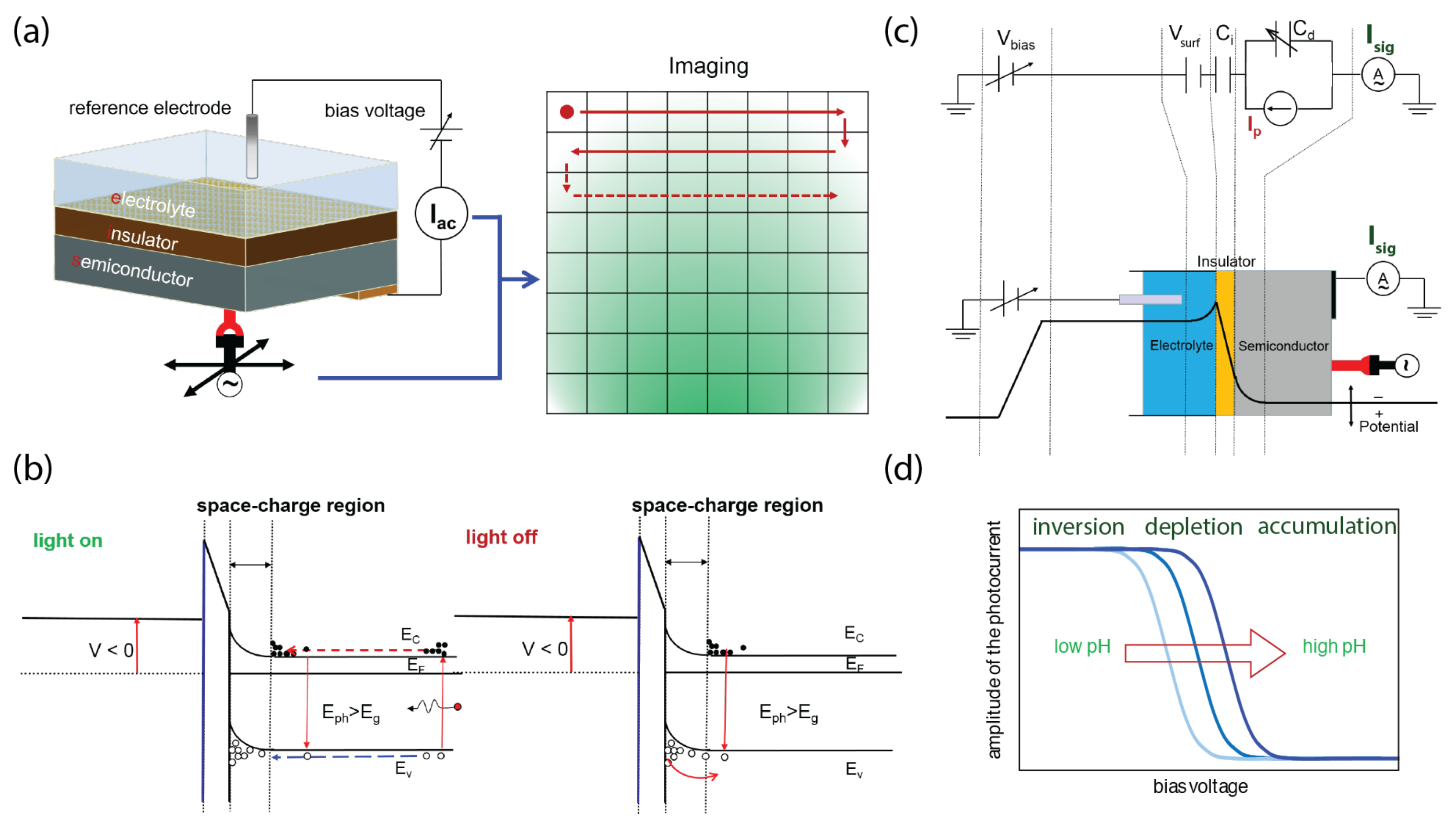
9]. A typical LAPS setup with an EIS structure consists of a sensor chip biased with a DC voltage and a modulated light probe as depicted in
Figure 1.
A bias voltage is applied across the sensor structure with a reference electrode and a backside ohmic contact to define the working point of the LAPS by inducing a space–charge region at the insulator-semiconductor interface (
Figure 1a). The surface potential, which depends on the local concentration of certain biochemical species, is superimposed to the bias voltage, which modifies the width of the space–charge region locally.
When this part of the semiconductor substrate is illuminated with a modulated light probe, a localized photocurrent is generated and detected in the external circuit. The amplitude and phase shift of the photocurrent are affected by the local surface potential of the illuminated region, and thus by the analyte concentration. Scanning the sensor plate with a light probe in a raster-line manner results in a spatial distribution of the surface potential, which represents a map of the concentration of the specific biochemical species.
The detailed mechanisms for the AC photocurrent generated are illustrated with energy band diagrams in
Figure 1b. The electron-hole pairs are induced upon illumination and they diffuse toward the depletion layer. The electrons and holes will then be separated by the electric field inside the depletion layer, which results in a transient current. When the light is off, the excess holes separated by the depletion electric field will recombine with the electrons, which results in a reverse transient current.
The working principle for the LAPS with a change in the sensing surface potential can be simplified into an equivalent circuit model, as shown in
Figure 1c. The photocurrent generated due to the separation of electron-hole pairs within the depletion layer is illustrated as
, and
represents the capacitance change as a function of the change in
, which results in a change in the measured LAPS signal
from the external circuit. The detectable photocurrent (
) can be simplified as:
This shows the dependence of
on the depletion capacitance,
. In addition to the simplified circuit diagram to describe the working mechanisms of the LAPS, a detailed physical model for the working principle for the LAPS was developed to understand the fundamental physical mechanisms, as well as optimize the parameters for enhanced sensing performance [
14,
15]. As an example, the variation in photocurrent (
) as a function of
is plotted in
Figure 1d, which shows the transition from inversion, depletion, and accumulation during LAPS sensing. The
versus
curve shifts with the analyte concentration—here, with pH as an example.
2.1.3. Biochemical Multiplexed and Imaging Applications
This light addressability equips the sensor with unique multiplexed chemical sensing and imaging abilities, the well-known application of which is to monitor the cell metabolism or bacterial growth by measurement of the extracellular acidification rate [
16,
17,
18,
19]. In addition, surface modification of the LAPS becomes easy and straightforward due to its large flat surface. For example, certain species, such as
,
, and
can be detected by the deposition of ion-sensitive membranes on the LAPS surface [
12,
13,
20].
Recent work [
13] on multi-parameter sensing has been performed based on the LAPS configuration, which can detect different types of ions sequentially (
Figure 2a). In addition, the surface of the LAPS, such as Si
N
or Ta
O
, have been demonstrated to have biocompatibility for cell culturing and can be used together with other techniques, such as magnetic beads loaded with specific drugs for pharmaceutical screening (
Figure 2b) [
21]. Moreover, label-free detection of DNA can also be realized by the immobilization of ssDNA probes on the LAPS surface [
22,
23,
24].
Recent advances in aptamer purification and isolation have further prompted the development of an aptamer-based LAPS sensing platform with ultra-high sensitivity and selectivity [
25,
26,
27]. This is because of the unique features of aptamer-enabled field-effect detection [
28], where all biochemical interactions occur within the Debye length for the electrolyte-insulator region, which magnifies the changes in the surface potential. Furthermore, a micrometer-scale LAPS chip was combined with optical fibers for glucose sensing [
29]. In this work, a probe-type LAPS and miniaturized LAPS measurement module were produced for the rapid determination of glucose in blood and urine. Not only limited to
applications,
application of LAPS has been shown to be possible when a miniaturized LAPS is combined with new types of fibers with electrical, optical, and electrochemical modalities integrated [
30,
31]. In this work, a millimeter-scale LAPS was combined with multifunctional fibers, and the possibility of recording both electrical activity and subtle pH changes in the hippocampus of both a healthy and diseased rat brain was demonstrated.
Fulfilling the need for such measurements, different types of measurement configurations have been developed in recent years with particular concern for the focusing and modulation of light beams with high flexibility and miniaturization.
Table 1 gives a summary of the important investigations and experimental setups.
2.2. Light-Addressable Electrode as Photochemical Sensor
2.2.1. Background
Voltammetry is a technique used to control the potential and measure the current. A current is generated by the transfer of electrons between the solution and the electrode via redox reaction with an applied potential at the electrode, and this is called a faradaic current. For example, amperometry is a voltammetric technique, where sensors measure the current generated by electrons transferred in a redox reaction on the electrodes under a constant potential maintained by a reference electrode.
Amperometric sensors have many advantages because they detect analytes with a low limit of detection, high speed, and high selectivity. Furthermore, numerous microelectrode arrays (MEAs) have been fabricated with the development of microelectromechanical systems (MEMS) that enable measurement of the local concentration of analytes reacted upon electrodes and offer electrochemical images by integration of the current and position information [
1,
2] (
Figure 3a). Electrochemical imaging is a powerful tool used to obtain addressable information from samples, particularly biotissues [
36].
Although a large number of densified microelectrodes provide more detailed information on the samples, it is difficult to precisely arrange electrical lines and electrode pads in a limited space to individually connect each electrode. To reduce the electrical lines, local redox cycling system-based [
37,
38,
39] and complementary metal-oxide-semiconductor (CMOS)-type [
40,
41,
42,
43] amperometric sensors have been developed with high spatial and temporal resolution.
Probe-type microelectrodes, the so-called scanning electrochemical microscope (SECM) [
44,
45,
46], similarly offer addressable electrochemical information with a high spatial resolution. However, these systems require a complicated fabrication process, voltage control, and precise positional control of the probes. As a proposed solution to these issues, photoelectrochemical sensors have attracted great attention due to their high sensitivity and selectivity (
Figure 3b).
In addition, by shining locally-focused light onto a semiconductor, local information on faradaic reactions is obtained without numerous lead lines (
Figure 3c). In this section, we review the principle and application of light-addressable electrode-based electrochemical sensing and imaging.
2.2.2. Principles
The basic principle of light-addressable electrodes (LAEs) is explained using photoelectrochemical catalysis and dye-sensitized solar cells. For LAEs, semiconductors are used for light absorption as with the LAPS. In contrast, the surface of the semiconductors used in the LAPS is insulated by a thin high-resistance layer; therefore, direct charge transfer does not occur across the semiconductor-solution interface.
In an LAE, a photon of energy that is sufficiently higher than the bandgap of the semiconductor, locally or entirely, irradiates the semiconductor from the front or back side, and electron-hole pairs are subsequently generated at the semiconductor–liquid interface (
Figure 4a) [
47]. For example, when n-type silicon is used as the semiconductor, electron-hole pairs are depleted at a potential more positive than the device flat-band potential, E
(the applied potential at which there is no SCL). Irradiation of the electrode with the appropriate light means that the charge carriers can be transferred across the interface.
The semiconductor in an unexcited area (the dark region) is depleted and shows high resistance at the interface; therefore, the redox species do not react under the applied potential. The electrochemical reaction can, thus, be locally induced only at the excitation area. Moreover, only a single lead line is required to measure the current with the redox reaction, which minimizes complications with regard to wiring.
Although a silicon substrate is often used as the semiconducting material for sensor substrates, other photoconductive materials (TiO
nanorods [
48], InGaN [
49], and ZnO [
50]) are applicable for LAE. Furthermore, semiconductor particles and molecules, such as metal oxide nanoparticles, quantum dots (QDs) [
51], polyaniline (PANI) [
52], dye molecules [
53], and graphitic-phase carbon nitride (g-C
N
) [
54], are also employed as photoactive semiconductors with the integration of a transparent conductive substrate (e.g., tin-doped indium oxide (ITO) and fluorine-doped tin oxide (FTO)).
2.2.3. Light-Addressable Electrodes (LAE) for Biosensing
Photoelectrochemical sensors have high sensitivity, are low cost, and require only simple instrumentation [
55,
56]; therefore, they are promising sensors for life science research and clinical diagnostics [
57,
58,
59], such as for the detection of molecules, proteins, antigens, antibodies, nucleic acids, and cells. Golub, Willner, and colleagues have developed DNA sensors based on photoelectrochemical devices with QDs as semiconductors [
60,
61,
62].
In this approach, CdS nanoparticles were used as the semiconductor, and double-stranded DNA-cross-linked CdS nanoparticle arrays on the electrode enhanced the photocurrent generation under irradiation. Recently, high-sensitivity photoelectrochemical sensors for DNA have been developed using approaches, such as wrinkled interfaces [
63] and plasmonic nanoparticles [
64]. These photoelectrochemical sensors facilitate the screening of biosamples using specific enzymes, antibodies, and aptamers as the targets.
Lv et al. recently developed ultrasensitive photoelectrochemical sensors modified with a specific aptamer for tumor biomarkers inspired by the light reaction of green plants with a Z-type photoinduced electron-transfer chain between two photosystems [
65]. The aptamer can be designed with respect to the target molecules by changing the base sequence, so that several molecules, including alpha-fetoprotein (AFP), carcinoembryonic antigen (CEA), cancer antigen 15-3 (CA 15-3), and human IgG could be evaluated.
Wang et al. proposed label-free, high-throughput sensing using light-addressable photoelectrochemical sensors [
66] and successfully evaluated multiple tumor markers on a single electrode by simply scanning with a green laser pen as the light source. In recent years, neurotransmitters were evaluated using LAEs [
59], which indicates that LAEs are adaptive for biological sensing, including for neuroscience.
The localized surface plasmonic resonance (LSPR) phenomenon in metallic nanostructures, including Au and Ag nanoparticles, is promising for improving the sensitivity for photoelectrochemical reactions. LSPR is a charge density oscillation on the surface of metal nanoparticles with a specific wavelength of the incident electromagnetic field, which results in enhancement of the electromagnetic fields around the nanoparticles [
67]. The photocatalytic activity and photocurrent are amplified under light irradiation at an appropriate wavelength depending on the species, size, and shape of the nanoparticles and the environment surrounding the particles [
68,
69,
70,
71].
Therefore, an appropriate combination of semiconductor and plasmonic metal enhances light absorbance and charge transfer at the semiconductor/metal interface [
72,
73]. Zhuang et al. reported plasmonic Au nanoparticles/g-C
N
nanohybrid-based photoelectrochemical sensors for monitoring polynucleotide kinase activity (
Figure 4b) [
54]. In this system, g-C
N
and Au nanoparticles were used as the molecular semiconductor and plasmonic metal, respectively, and the sensitivity of the sensor was doubled by modification with the Au nanoparticles due to their LSPR properties.
2.2.4. LAE as a Photoelectrochemical Imaging Sensor
Photoelectrochemical sensors are applicable to spatially-resolved biochemical reactions via the addressable light source and scanning of the light spot [
74,
75,
76,
77,
78]. In 1983, Butler first reported photoelectrochemical imaging to obtain grain boundary information on titanium at a constant applied potential [
79]. The system consisted of an x–y stage, a laser source, a laser scanning system, and a three-electrode system connected to a titanium substrate, whereby variations in electronic properties depending on the metal grain structure were observed.
In 2010, the Tao group successfully imaged heterogeneous surfaces using a local electrochemical current with LSPR under partial light irradiation [
80]. Such photoelectrochemical imaging systems, enabled via an addressable light, have been rapidly improved with the development of new photoelectrochemical sensors, stable semiconductor surfaces, and laser manipulation.
Ciampi’s group recently fabricated oxide-free silicon by the modification of a hydrogen-terminated silicon surface with a monolayer of a dialkyne to prevent oxidation [
47,
81,
82]. In addition, a ferrocene-containing azide group was introduced onto the surface via a copper-catalyzed azide-alkyne cycloaddition reaction to accelerate the redox reaction at the interface. Ciampi’s group recently reported the microfabrication of Cu
O silicon [
83,
84], for the imaging of methanol oxidation upon electrocatalysis (
Figure 5a) [
85].
Currently, cellular manipulation has been successfully demonstrated using light-addressable photoelectrochemical devices modified with electrochemically cleavable antibodies [
86]. The LAE is a promising system for the imaging of cellular morphology and activity. The Krause group recently reported a photoelectrochemical imaging system to monitor cell lysis with a surfactant (
Figure 5b) [
87,
88].
This system monitors the oxidation of hydroxide ions to hydroxyl radicals on a photoactivated electrode. The diffusion of hydroxide ions is blocked under the cells; therefore, the photocurrent is decreased more than that for an unblocked area. Two-dimensional imaging applications of photoelectrochemical imaging systems enabled by addressable light have significant potential for the estimation of local cellular activity, such as the differentiation of stem cells, the release of neurotransmitters, and oxygen consumption, although further improvements of the sensitivity, selectivity, and frame rate of the imaging devices are required.
3. Light Readable Electrochemistry
The light emitting phenomenon caused by the electrochemical reaction of specific molecule species, called luminophores, is known as electrogenerated chemiluminescence or electrochemiluminescence (ECL). In 1990, Leland and Powell first reported ECL generated from the electrochemical reaction of
and tripropylamine(TPA), one of the most widely used luminophores today [
89].
Unlike luminescence by fluorescent molecules, the ECL requires no excitation light for light emission and is simply generated by an electrochemical reaction on the electrode surface, which results in ease of handling and low background noise. Furthermore, ECL has high spatial and temporal resolution and enables high-throughput sensing using a simple instrument setup: a camera as a readout tool and a three-electrode system to control the voltage [
90,
91].
3.1. Application of Electrochemiluminescence for Sensing and Imaging
The ECL has features, such as a high signal-to-noise ratio, high spatial resolution, high throughput, and ease of handling; therefore, many applications have been proposed for sensors and for imaging systems for diagnostic and life science research.
Various methods for the sensing of biomarkers have been applied using the ECL. For example, luminophore molecules can be combined with metal nanoparticles (e.g., gold nanoparticles) and antibodies. Labeling with such a complex on a target antigen enables immunoassay based on detection of the ECL intensity of the antigen (
Figure 6a,b) [
92,
93,
94,
95,
96,
97]. Biomolecule detection using luminol/hydrogen peroxide has also been reported.
Luminol/hydrogen peroxide is a major luminophore system, similar as the
and tripropylamine(TPA) system. Hydrogen peroxide, which is a biomolecule itself, is used as a co-reactant with luminol, and thereby the detection of hydrogen peroxide [
98] and other biomolecules with combinations of enzymatic reactions is possible. Xu et al. successfully measured the glucose concentration released from a single cell by the ECL intensity of luminol through the conversion of released glucose into hydrogen peroxide by the glucose oxidase enzymatic reaction [
99].
In addition, such ECL detection mechanisms can also be used for the imaging of biomolecules, proteins, and cell-matrix adhesion [
100,
101,
102,
103,
104,
105,
106]. For example, labeling of the luminophore molecules on the surface of a cell membrane via metal nanoparticles and proteins enables visualization of the cell membrane topology on the electrode (
Figure 6c) [
100].
The luminescence mechanism for luminol/hydrogen peroxide makes it possible to image the distribution of biomolecules, including hydrogen peroxide, released from cells [
103,
104,
105]. Hiramoto et al. succeeded in imaging the respiratory activity of cell spheroids by observing the decrease of ECL caused by depletion of the oxygen concentration (
Figure 6d) [
106]. Here, the ECL was generated from the reaction of luminol with hydrogen peroxide generated by the reduction reaction of dissolved oxygen on the electrode. The ECL is, thus, widely applied as a simple, high-sensitivity sensing and imaging system.
3.2. Sensing Systems Using Closed Bipolar Electrode/ECL
There are many reports of sensing systems that combine ECL with a closed bipolar electrode (cBPE) system [
107,
108,
109,
110,
111]. The cBPE system consists of an electrode, the so called BPE, which is in contact with two physically divided solutions at both poles, and driving electrodes are inserted into each individual solution. When a sufficient driving potential is applied between the driving electrodes through the two solutions, oxidation and reduction reactions are simultaneously induced on both poles of the cBPE without connection from an external power source.
In a sensing system that combines a cBPE and ECL, one pole of the cBPE is in contact with the measurement solution, which includes the target molecules or object. On the other hand, the opposite pole of the cBPE is in contact with a luminophore solution. The intensity of ECL is proportional to the electrochemical reaction of the analyte on the opposite pole; therefore, ECL can be used to quantify the analyte concentration by monitoring the light emission using a readout camera (
Figure 7a).
3.3. Microscopic Systems Based on cBPE/ ECL
In recent years, attempts have been made to extend the cBPE/ECL sensing system to a microscopic system for the two-dimensional imaging of molecule concentration distributions [
112,
113,
114,
115,
116,
117,
118]. These microscopic systems are based on a cBPE array that consists of vertically arranged cBPEs. The distribution of sample molecules on one side of the cBPE array can be visualized with ECL signals generated from the opposite side (
Figure 7b).
As noted in
Section 2.2.1, although conventional electrochemical imaging systems, such as SECM and MEA, have high spatial and temporal resolution, respectively, SECM requires a complicated fabrication process, voltage control, and precise position control of the probes, while MEA generally requires electrical lines on the individual electrodes, which limits the electrode density. In contrast, BPE can be arranged at a high density on a single plate because it does not require a connection to a potentiostat. Moreover, the ECL signal is monitored at high temporal resolution due to the simultaneous electrochemical reactions at both ends of the cBPE.
In 2014, Oja and Zhang demonstrated the two-dimensional concentration distribution mapping of sample molecules using fluorescent signals [
119]. In 2017, Zhai et al. reported a sensing platform using ECL for the measurement of molecules, such as hydrogen peroxide, with a cBPE array made of a nanoporous membrane filled with gold [
109]. As an early attempt at a microscopic system using a cBPE array and ECL signals, Eßmann et al. developed scanning bipolar electrochemical microscopy (SBECM) using a cBPE array probe that incorporated seven cBPEs in a single probe, which enabled imaging at high spatial resolution (50
m) in real time by probe scanning [
112].
Iwama et al. demonstrated a proof-of-concept for a bipolar electrochemical microscopy (BEM) system by imaging the dynamics of the concentration distribution of sample molecules in real time using a simple cBPE array in which 61 gold wires were bundled (300
m diameter, electrode pitch 400
m) [
113].
To realize high spatial resolution imaging at the micro-nanoscale, micro-/nanofabricated cBPEs were densely arranged as an array. Anderson et al. succeeded in producing a cBPE array in which >14,000 carbon microelectrodes were uniformly arranged with an electrode spacing of 28 μm by insulating carbon micropillars produced by the pyrolysis of SU-8. They achieved imaging of the molecular concentration of the sample (
Figure 7c) [
115]. Iwama et al. developed a cBPE array in which cBPEs were randomly arranged at an average pitch of 41 μm by depositing gold inside a microporous membrane [
116].
Qin et al. recently achieved imaging at the nanoscale using a cBPE array that was highly densified by the electrodeposition of gold nanowires on an anodic aluminum oxide (AAO) membrane, in which 200 nm diameter nanopores were arranged with a pitch of 450 nm. This nanoscale cBPE array was used to demonstrate imaging of the hydrogen evolution reaction catalyzed by single platinum nanoparticles (
Figure 7d) [
117].
Various types of microscopic systems that use scanning cBPE array probes and cBPE arrays with ECL signals have, thus, been proposed, as well as methods for the fabrication of high-density cBPE arrays. In principle, it will be possible to image sample molecular concentrations up to the diffraction limit of light, as long as the resolution of the camera allows.
3.4. Application for Bioimaging
A microscopic system that uses a cBPE array and ECL can track a molecular concentration without the need for a fluorescent molecular probe, which enables the direct, label-free analysis of biomolecules without the exposure of the biological sample to fluorescent molecular probes. Santos et al. proposed the applicability of SBECM to cellular respiratory activity imaging. Here, SBECM was used to successfully monitor the oxygen concentration difference caused by the sample topography and the photoelectrocatalytic reaction of Mo-doped
(
Figure 8a) [
114].
Iwama et al. achieved imaging of the respiration activity of MCF-7 spheroids using BEM and showed the applicability for label-free bioimaging (
Figure 8b) [
116]. This group also succeeded in imaging the concentration distribution of dopamine, the major neurotransmitter that plays an important role in nerve cell function by employing a cathodic luminophore (
Figure 8c) [
118]. In conventional cBPE/ECL systems, the available luminophores have ECL generated through an oxidation reaction. Therefore, the molecules that can be analyzed have been limited to those that undergo a reduction reaction at the opposite pole of the cBPE. This group expanded the selection pools of analytes. In the future, further expansion of the target molecules can be expected through the use of, for example, enzymatic modification of the cBPE array. This may lead to imaging of various biological phenomena with a high spatiotemporal resolution.
4. Conclusions
We reviewed light-addressable and light-readable electrochemical systems and discussed their working principles and promising applications, particularly in obtaining spatially-resolved electrochemical information via a focused light beam. In conventional electrode-based electrochemistry, the electrode size defines the spatially obtainable information for a localized electrochemical reaction. Upon the construction of an electrode array, the mapping of electrochemical information can be possible; however, it suffers from wiring complications.
The introduction of light into electrochemistry enables a new measurement paradigm to obtain spatially-resolved electrochemical information with a simple electrical readout. In particular, light-addressable sensors, such as LAPS and LAE, which are based on semiconductor materials, are activated with localized light due to the photoelectronic effect. The induced localized photocurrent is monitored through a single lead line. The LAPS and the LAE offer a versatile platform for the label-free imaging of various biochemicals in both and settings.
Not only limited to measurement, an LAE can directly interact with the electrolyte via the faradaic current, which enables the manipulation of electrochemical reactions, such as cellular stimulation and collection, and microfabrication using the addressable light. In light-readable sensors, the luminescence locally generated on the electrode via an electrochemical reaction is monitored with the aid of optical microscopy. The high sensitivity and high spatiotemporal resolution enabled by the ECL detection mechanisms means that label-free ECL imaging systems can be widely applied in biochemical investigations.
We demonstrated promising applications of these systems to obtain detailed biochemical information in a spatially-resolved manner. However, these systems still suffer from various shortcomings that demand future research. For light-addressable systems, the primary constraint to achieving high spatiotemporal resolution is the engineering challenge to effectively focus and modulate the light beam. For light-readable systems, the immersion of biological samples in luminophore solution for ECL analysis carries a concern of toxicity with respect to the luminophore and its co-reactant.
Future directions concerning the involvement of light in electrochemistry are leading to both detection and manipulation systems with simultaneous multi-parameter detection, enhanced selectivity, high spatiotemporal resolution imaging, and biocompatability. Light will, thus, illuminate the future of electrochemistry.
Author Contributions
H.A., T.I., and Y.G. conceived the idea and contributed to investigations and writing equally. H.A. and Y.G. managed the project administration and funding acquisition. All authors have read and agreed to the published version of the manuscript.
Funding
This research was funded by the Japan Society for the Promotion of Science (JSPS) (Nos. 19K15598 and 19J20709), the Japan Science and Technology Agency (JST) (FOREST Program (No. JPMJFR205D) and a JST COI Grant Number JPMJCE1303.), and the FRIS Creative Interdisciplinary Collaboration Program at Tohoku University.
Institutional Review Board Statement
Not applicable.
Informed Consent Statement
Not applicable.
Data Availability Statement
Not applicable.
Acknowledgments
H.A. wishes to acknowledge funding in the form of a Kakenhi Grant-in-Aid (No. 19K15598) from the Japan Society for the Promotion of Science (JSPS) and the FRIS Creative Interdisciplinary Collaboration Program at Tohoku University. T.I. acknowledges a Grant-in-Aid for JSPS Fellows (No. 19J20709). Y.G. would like to thank the support from the Japan Science and Technology Agency (JST) FOREST Program (No. JPMJFR205D) and a JST COI Grant Number JPMJCE1303.
Conflicts of Interest
The authors declare no conflict of interests regarding the work presented in this article.
Abbreviations
The following abbreviations are used in this manuscript:
| LAPS | Light-addressable potentiometric sensor |
| LAE | Light-addressable electrode |
| MEA | Microelectrode array |
| MEMS | Micro electromechanical systems |
| CMOS | Complementary metal-oxide-semiconductor |
| LSPR | Localized surface plasmon resonance |
| cBPE | Closed bipolar electrode |
| ECL | Electrochemiluminescence |
| SECM | Scanning electrochemical microscopy |
| SBECM | Scanning bipolar electrochemical microscopy |
| BEM | Bipolar electrochemical microscopy |
References
- Sassa, F.; Biswas, G.C.; Suzuki, H. Microfabricated electrochemical sensing devices. Lab Chip 2020, 20, 1358–1389. [Google Scholar] [CrossRef]
- Wang, J.; Trouillon, R.; Lin, Y.; Svensson, M.I.; Ewing, A.G. Individually addressable thin-film ultramicroelectrode array for spatial measurements of single vesicle release. Anal. Chem. 2013, 85, 5600–5608. [Google Scholar] [CrossRef] [PubMed]
- Vogel, Y.B.; Gooding, J.J.; Ciampi, S. Light-addressable electrochemistry at semiconductor electrodes: Redox imaging, mask-free lithography and spatially resolved chemical and biological sensing. Chem. Soc. Rev. 2019, 48, 3723–3739. [Google Scholar] [CrossRef] [PubMed]
- Welden, R.; Schöning, M.J.; Wagner, P.H.; Wagner, T. Light-addressable electrodes for dynamic and flexible addressing of biological systems and electrochemical reactions. Sensors 2020, 20, 1680. [Google Scholar] [CrossRef] [Green Version]
- Yoshinobu, T.; Miyamoto, K.i.; Werner, C.F.; Poghossian, A.; Wagner, T.; Schöning, M.J. Light-addressable potentiometric sensors for quantitative spatial imaging of chemical species. Annu. Rev. Anal. Chem. 2017, 10, 225–246. [Google Scholar] [CrossRef] [PubMed]
- Bergveld, P. Development of an Ion-Sensitive Solid-State Device for Neurophysiological Measurements. IEEE Trans. Biomed. Eng. 1970, 17, 70–71. [Google Scholar] [CrossRef]
- Poghossian, A.; Yoshinobu, T.; Simonis, A.; Ecken, H.; Lüth, H.; Schöning, M. Penicillin detection by means of field-effect based sensors: EnFET, capacitive EIS sensor or LAPS. Sens. Actuators B 2001, 78, 237–242. [Google Scholar] [CrossRef]
- Engström, O.; Alm, A. Energy concepts of insulator-semiconductor interface traps. Jpn. J. Appl. Phys. 1983, 54, 5240–5244. [Google Scholar] [CrossRef]
- Hafeman, D.; Parce, J.; McConnell, H. Light-addressable potentiometric sensor for biochemical systems. Science 1988, 240, 1182–1185. [Google Scholar] [CrossRef] [PubMed]
- Miyamoto, K.; Kaneko, K.; Matsuo, A.; Wagner, T.; Kanoh, S.; Schöning, M.; Yoshinobu, T. Miniaturized chemical imaging sensor system using an OLED display panel. Sens. Actuators B 2010, 170, 82–87. [Google Scholar] [CrossRef]
- Wagner, T.; Werner, C.; Miyamoto, K.; Schöning, M.; Yoshinobu, T. Development and characterisation of a compact light-addressable potentiometric sensor (LAPS) based on the digital light processing (DLP) technology for flexible chemical imaging. Sens. Actuators B 2012, 170, 34–39. [Google Scholar] [CrossRef]
- Yoshinobu, T.; Iwasaki, H.; Ui, Y.; Furuichi, K.; Ermolenko, Y.; Mourzina, Y.; Wagner, T.; Näther, N.; Schöning, M. The light-addressable potentiometric sensor for multi-ion sensing and imaging. Methods 2005, 37, 94–102. [Google Scholar] [CrossRef] [PubMed]
- Liang, T.; Jiang, N.; Zhou, S.; Wang, X.; Xu, Y.; Wu, C.; Kirsanov, D.; Legin, A.; Wan, H.; Wang, P. Multiplexed All-Solid-State Ion-Sensitive Light-Addressable Potentiometric Sensor (ISLAPS) System Based on Silicone-Rubber for Physiological Ions Detection. Anal. Chim. Acta 2021, 1179, 338603. [Google Scholar] [CrossRef]
- Guo, Y.; Miyamoto, K.i.; Wagner, T.; Schöning, M.J.; Yoshinobu, T. Device simulation of the light-addressable potentiometric sensor for the investigation of the spatial resolution. Sens. Actuators B Chem. 2014, 204, 659–665. [Google Scholar] [CrossRef]
- Guo, Y.; Miyamoto, K.i.; Wagner, T.; Schöning, M.J.; Yoshinobu, T. Theoretical study and simulation of light-addressable potentiometric sensors. Phys. Status Solidi 2014, 211, 1467–1472. [Google Scholar] [CrossRef]
- Parak, W.; George, M.; Domke, J.; Radmacher, M.; Behrends, J.; Denyer, M.; Gaub, H. Can the Light-Addressable Potentiometric Sensor (LAPS) Detect Extracellular Potentials of Cardiac Myocytes? IEEE Trans. Biomed. Eng. 2000, 47, 1106–1113. [Google Scholar] [CrossRef] [PubMed]
- McConnell, H.; Owicki, J.; Parce, J.; Miller, D.; Baxter, G.; Wada, H.; Pitchford, S. The Cytosensor Microphysiometer: Biological Applications of Silicon Technology. Science 1992, 257, 1906–1912. [Google Scholar] [CrossRef]
- Xu, G.; Ye, X.; Qin, L.; Xu, Y.; Li, Y.; Li, R.; Wang, P. Cell-based biosensors based on light-addressable potentiometric sensors for single cell monitoring. Biosens. Bioelectron. 2005, 20, 1757–1763. [Google Scholar] [CrossRef]
- Dantism, S.; Röhlen, D.; Wagner, T.; Wagner, P.; Schöning, M.J. A laps-based differential sensor for parallelized metabolism monitoring of various bacteria. Sensors 2019, 19, 4692. [Google Scholar] [CrossRef] [Green Version]
- Yang, J.; Lu, T.; Wang, J.; Yang, C.; Pijanowska, D.; Chin, C.; Lue, C.; Lai, C. LAPS with nanosacled and highly polarized HfO2 by CF4 plasma for NH4+ detection. Sens. Actuators B 2013, 180, 71–76. [Google Scholar] [CrossRef]
- Wagner, T.; Vornholt, W.; Werner, C.F.; Yoshinobu, T.; Miyamoto, K.i.; Keusgen, M.; Schöning, M.J. Light-addressable potentiometric sensor (LAPS) combined with magnetic beads for pharmaceutical screening. Phys. Med. 2016, 1, 2–7. [Google Scholar] [CrossRef] [Green Version]
- Kataoka-Hamai, C.; Miyahara, Y. Label-Free Detection of DNA by Field-Effect Devices. IEEE Sens. J. 2011, 11, 3153–3160. [Google Scholar] [CrossRef]
- Wu, C.; Bronder, T.; Poghossian, A.; Werner, C.F.; Schöning, M.J. Label-free detection of DNA using a light-addressable potentiometric sensor modified with a positively charged polyelectrolyte layer. Nanoscale 2015, 7, 6143–6150. [Google Scholar] [CrossRef]
- Wu, C.; Poghossian, A.; Bronder, T.S.; Schöning, M.J. Sensing of double-stranded DNA molecules by their intrinsic molecular charge using the light-addressable potentiometric sensor. Sens. Actuators B Chem. 2016, 229, 506–512. [Google Scholar] [CrossRef]
- Li, F.; Hu, S.; Zhang, R.; Gu, Y.; Li, Y.; Jia, Y. Porous graphene oxide enhanced aptamer specific circulating-tumor-cell sensing interface on light addressable potentiometric sensor: Clinical application and simulation. ACS Appl. Mater. Interfaces 2019, 11, 8704–8709. [Google Scholar] [CrossRef]
- Wu, C.; Du, L.; Zou, L.; Zhao, L.; Wang, P. An ATP sensitive light addressable biosensor for extracellular monitoring of single taste receptor cell. Biomed. Microdevices 2012, 14, 1047–1053. [Google Scholar] [CrossRef] [PubMed]
- Du, L.; Wang, J.; Chen, W.; Zhao, L.; Wu, C.; Wang, P. Dual functional extracellular recording using a light-addressable potentiometric sensor for bitter signal transduction. Anal. Chim. Acta 2018, 1022, 106–112. [Google Scholar] [CrossRef]
- Nakatsuka, N.; Yang, K.A.; Abendroth, J.M.; Cheung, K.M.; Xu, X.; Yang, H.; Zhao, C.; Zhu, B.; Rim, Y.S.; Yang, Y.; et al. Aptamer–field-effect transistors overcome Debye length limitations for small-molecule sensing. Science 2018, 362, 319–324. [Google Scholar] [CrossRef]
- Zhang, W.; Liu, C.; Zou, X.; Zhang, H.; Xu, X. Micrometer-scale light-addressable potentiometric sensor on an optical fiber for biological glucose determination. Anal. Chim. Acta 2020, 1123, 36–43. [Google Scholar] [CrossRef] [PubMed]
- Guo, Y.; Werner, C.F.; Canales, A.; Yu, L.; Jia, X.; Anikeeva, P.; Yoshinobu, T. Polymer-fiber-coupled field-effect sensors for label-free deep brain recordings. PLoS ONE 2020, 15, e0228076. [Google Scholar] [CrossRef]
- Guo, Y.; Werner, C.F.; Handa, S.; Wang, M.; Ohshiro, T.; Mushiake, H.; Yoshinobu, T. Miniature multiplexed label-free pH probe in vivo. Biosens. Bioelectron. 2021, 174, 112870. [Google Scholar] [CrossRef]
- Schöning, M.; Wagner, T.; Wang, C.; Otto, R.; Yoshinobu, T. Development for a handheld 16 chnnel pen-type LAPS for electrochemical sensing. Sens. Actuators B 2005, 108, 808–814. [Google Scholar] [CrossRef]
- Wagner, T.; C. Rao, J.K.; Yoshinobu, T.; Otto, R.; Keusgen, M.; Schöning, M. “LAPS Card”—A novel chip card-based light-addressable potentiometric sensor (LAPS). Sens. Actuators B 2006, 118, 33–40. [Google Scholar] [CrossRef]
- Das, A.; Chen, T.C.; Yang, C.M.; Lai, C.S. A high-speed, flexible-scanning chemical imaging system using a light-addressable potentiometric sensor integrated with an analog micromirror. Sens. Actuators B Chem. 2014, 198, 225–232. [Google Scholar] [CrossRef]
- Yang, C.M.; Yen, T.H.; Liu, H.L.; Lin, Y.J.; Lin, P.Y.; Tsui, L.S.; Chen, C.H.; Chen, Y.P.; Hsu, Y.C.; Lo, C.H.; et al. A real-time mirror-LAPS mini system for dynamic chemical imaging and cell acidification monitoring. Sens. Actuators B Chem. 2021, 341, 130003. [Google Scholar] [CrossRef]
- Kasai, N.; Han, C.; Torimitsu, K. Hydrogen peroxide distribution and neuronal cell death in a rat hippocampal slice. Sens. Actuators B Chem. 2005, 108, 746–750. [Google Scholar] [CrossRef]
- Ino, K.; Nishijo, T.; Arai, T.; Kanno, Y.; Takahashi, Y.; Shiku, H.; Matsue, T. Local Redox-Cycling-Based Electrochemical Chip Device with Deep Microwells for Evaluation of Embryoid Bodies. Angew. Chem. 2012, 124, 6752–6756. [Google Scholar] [CrossRef]
- Ino, K.; Saito, W.; Koide, M.; Umemura, T.; Shiku, H.; Matsue, T. Addressable electrode array device with IDA electrodes for high-throughput detection. Lab Chip 2011, 11, 385–388. [Google Scholar] [CrossRef]
- Kätelhön, E.; Mayer, D.; Banzet, M.; Offenhäusser, A.; Wolfrum, B. Nanocavity crossbar arrays for parallel electrochemical sensing on a chip. Beilstein J. Nanotechnol. 2014, 5, 1137–1143. [Google Scholar] [CrossRef] [Green Version]
- Kim, B.N.; Herbst, A.D.; Kim, S.J.; Minch, B.A.; Lindau, M. Parallel recording of neurotransmitters release from chromaffin cells using a 10 × 10 CMOS IC potentiostat array with on-chip working electrodes. Biosens. Bioelectron. 2013, 41, 736–744. [Google Scholar] [CrossRef] [PubMed] [Green Version]
- Abe, H.; Ino, K.; Li, C.Z.; Kanno, Y.; Inoue, K.Y.; Suda, A.; Kunikata, R.; Matsudaira, M.; Takahashi, Y.; Shiku, H.; et al. Electrochemical imaging of dopamine release from three-dimensional-cultured PC12 cells using large-scale integration-based amperometric sensors. Anal. Chem. 2015, 87, 6364–6370. [Google Scholar] [CrossRef]
- Abe, H.; Yabu, H.; Kunikata, R.; Suda, A.; Matsudaira, M.; Matsue, T. Redox cycling-based electrochemical CMOS imaging sensor for real time and selective imaging of redox analytes. Sens. Actuators B Chem. 2020, 304, 127245. [Google Scholar] [CrossRef]
- Bellin, D.L.; Sakhtah, H.; Zhang, Y.; Price-Whelan, A.; Dietrich, L.E.; Shepard, K.L. Electrochemical camera chip for simultaneous imaging of multiple metabolites in biofilms. Nat. Commun. 2016, 7, 10535. [Google Scholar] [CrossRef] [PubMed] [Green Version]
- Bard, A.J.; Mirkin, M.V. Scanning Electrochemical Microscopy; CRC Press: Boca Raton, FL, USA, 2001. [Google Scholar]
- Actis, P.; Tokar, S.; Clausmeyer, J.; Babakinejad, B.; Mikhaleva, S.; Cornut, R.; Takahashi, Y.; López Córdoba, A.; Novak, P.; Shevchuck, A.I.; et al. Electrochemical nanoprobes for single-cell analysis. ACS Nano 2014, 8, 875–884. [Google Scholar] [CrossRef] [Green Version]
- Takahashi, Y.; Kumatani, A.; Shiku, H.; Matsue, T. Scanning probe microscopy for nanoscale electrochemical imaging. Anal. Chem. 2017, 89, 342–357. [Google Scholar] [CrossRef]
- Choudhury, M.H.; Ciampi, S.; Yang, Y.; Tavallaie, R.; Zhu, Y.; Zarei, L.; Gonçales, V.R.; Gooding, J.J. Connecting electrodes with light: One wire, many electrodes. Chem. Sci. 2015, 6, 6769–6776. [Google Scholar] [CrossRef] [Green Version]
- Feng, J.; Yang, P.; Wang, S.; Wang, J. Photoelectrochemical chiral sensing on the basis of TiO2–metal complex hybrid film. J. Electroanal. Chem. 2012, 674, 97–102. [Google Scholar] [CrossRef]
- Zhou, B.; Das, A.; Kappers, M.J.; Oliver, R.A.; Humphreys, C.J.; Krause, S. InGaN as a Substrate for AC Photoelectrochemical Imaging. Sensors 2019, 19, 4386. [Google Scholar] [CrossRef] [Green Version]
- Tu, Y.; Ahmad, N.; Briscoe, J.; Zhang, D.W.; Krause, S. Light-addressable potentiometric sensors using ZnO nanorods as the sensor substrate for bioanalytical applications. Anal. Chem. 2018, 90, 8708–8715. [Google Scholar] [CrossRef] [PubMed] [Green Version]
- Yue, Z.; Lisdat, F.; Parak, W.J.; Hickey, S.G.; Tu, L.; Sabir, N.; Dorfs, D.; Bigall, N.C. Quantum-dot-based photoelectrochemical sensors for chemical and biological detection. ACS Appl. Mater. Interfaces 2013, 5, 2800–2814. [Google Scholar] [CrossRef]
- Zhu, J.; Huo, X.; Liu, X.; Ju, H. Gold nanoparticles deposited polyaniline—TiO2 nanotube for surface plasmon resonance enhanced photoelectrochemical biosensing. ACS Appl. Mater. Interfaces 2016, 8, 341–349. [Google Scholar] [CrossRef]
- Li, Y.; Chen, F.Z.; Xu, Y.T.; Yu, W.J.; Li, H.Y.; Fan, G.C.; Han, D.M.; Zhao, W.W.; Jiang, D.C. Self-assembled peptide nanostructures for photoelectrochemical bioanalysis application: A proof-of-concept study. Anal. Chem. 2019, 91, 12606–12610. [Google Scholar] [CrossRef] [Green Version]
- Zhuang, J.; Lai, W.; Xu, M.; Zhou, Q.; Tang, D. Plasmonic AuNP/g-C3N4 nanohybrid-based photoelectrochemical sensing platform for ultrasensitive monitoring of polynucleotide kinase activity accompanying DNAzyme-catalyzed precipitation amplification. ACS Appl. Mater. Interfaces 2015, 7, 8330–8338. [Google Scholar] [CrossRef]
- Zhao, W.W.; Xu, J.J.; Chen, H.Y. Photoelectrochemical bioanalysis: The state of the art. Chem. Soc. Rev. 2015, 44, 729–741. [Google Scholar] [CrossRef] [PubMed]
- Shu, J.; Tang, D. Recent advances in photoelectrochemical sensing: From engineered photoactive materials to sensing devices and detection modes. Anal. Chem. 2019, 92, 363–377. [Google Scholar] [CrossRef] [PubMed]
- Wang, Z.; Liu, J.; Liu, X.; Shi, X.; Dai, Z. Photoelectrochemical approach to apoptosis evaluation via multi-functional peptide-and electrostatic attraction-guided excitonic response. Anal. Chem. 2018, 91, 830–835. [Google Scholar] [CrossRef] [PubMed]
- Tang, J.; Kong, B.; Wang, Y.; Xu, M.; Wang, Y.; Wu, H.; Zheng, G. Photoelectrochemical detection of glutathione by IrO2-Hemin-TiO2 nanowire arrays. Nano Lett. 2013, 13, 5350–5354. [Google Scholar] [CrossRef]
- Terrero Rodríguez, I.M.; Borrill, A.J.; Schaffer, K.J.; Hernandez, J.B.; O’Neil, G.D. Light-addressable electrochemical sensing with electrodeposited n-silicon/gold nanoparticle Schottky junctions. Anal. Chem. 2020, 92, 11444–11452. [Google Scholar] [CrossRef]
- Peng, X.; Schlamp, M.C.; Kadavanich, A.V.; Alivisatos, A.P. Epitaxial growth of highly luminescent CdSe/CdS core/shell nanocrystals with photostability and electronic accessibility. J. Am. Chem. Soc. 1997, 119, 7019–7029. [Google Scholar] [CrossRef]
- Golub, E.; Pelossof, G.; Freeman, R.; Zhang, H.; Willner, I. Electrochemical, photoelectrochemical, and surface plasmon resonance detection of cocaine using supramolecular aptamer complexes and metallic or semiconductor nanoparticles. Anal. Chem. 2009, 81, 9291–9298. [Google Scholar] [CrossRef]
- Willner, I.; Patolsky, F.; Wasserman, J. Photoelectrochemistry with controlled DNA-cross-linked CdS nanoparticle arrays. Angew. Chem. 2001, 113, 1913–1916. [Google Scholar] [CrossRef]
- Saha, S.; Chan, Y.; Soleymani, L. Enhancing the photoelectrochemical response of DNA biosensors using wrinkled interfaces. ACS Appl. Mater. Interfaces 2018, 10, 31178–31185. [Google Scholar] [CrossRef]
- Victorious, A.; Saha, S.; Pandey, R.; Soleymani, L. Enhancing the sensitivity of photoelectrochemical DNA biosensing using plasmonic DNA barcodes and differential signal readout. Angew. Chem. Int. Ed. 2021, 60, 7316–7322. [Google Scholar] [CrossRef] [PubMed]
- Lv, S.; Zhang, K.; Zeng, Y.; Tang, D. Double photosystems-based ‘Z-Scheme’photoelectrochemical sensing mode for ultrasensitive detection of disease biomarker accompanying three-dimensional DNA walker. Anal. Chem. 2018, 90, 7086–7093. [Google Scholar] [CrossRef] [PubMed]
- Wang, J.; Long, J.; Liu, Z.; Wu, W.; Hu, C. Label-free and high-throughput biosensing of multiple tumor markers on a single light-addressable photoelectrochemical sensor. Biosens. Bioelectron. 2017, 91, 53–59. [Google Scholar] [CrossRef] [PubMed]
- de Souza, M.L.; dos Santos, D.P.; Corio, P. Localized surface plasmon resonance enhanced photocatalysis: An experimental and theoretical mechanistic investigation. RSC Adv. 2018, 8, 28753–28762. [Google Scholar] [CrossRef] [Green Version]
- Awazu, K.; Fujimaki, M.; Rockstuhl, C.; Tominaga, J.; Murakami, H.; Ohki, Y.; Yoshida, N.; Watanabe, T. A plasmonic photocatalyst consisting of silver nanoparticles embedded in titanium dioxide. J. Am. Chem. Soc. 2008, 130, 1676–1680. [Google Scholar] [CrossRef] [PubMed]
- Liu, Y.; Chen, F.; Wang, Q.; Wang, J.; Wang, J.; Gebremariam, T.T. Surface plasmon-enhanced activity and stability for methanol oxidation on gold caviar-like assembly under solar light. J. Mater. Chem. A 2018, 6, 10515–10524. [Google Scholar] [CrossRef]
- Huang, L.; Zou, J.; Ye, J.Y.; Zhou, Z.Y.; Lin, Z.; Kang, X.; Jain, P.K.; Chen, S. Synergy between Plasmonic and Electrocatalytic activation of methanol oxidation on palladium–silver alloy nanotubes. Angew. Chem. 2019, 131, 8886–8890. [Google Scholar] [CrossRef]
- Contreras, E.; Palacios, C.; Huerta, B.; Ahn, S.; Vazquez-Mena, O.; Cadena-Nava, R.D.; Alonso-Nunez, G.; Contreras, O.E.; Oropeza-Guzmán, M.T.; Romo-Herrera, J.M. Anodes for Direct Alcohol Fuel Cells Assisted by Plasmon-Accelerated Electrochemical Oxidation Using Gold Nanoparticle-Decorated Buckypapers. ACS Appl. Energy Mater. 2020, 3, 8755–8764. [Google Scholar] [CrossRef]
- Li, J.; Tu, W.; Li, H.; Han, M.; Lan, Y.; Dai, Z.; Bao, J. In situ-generated nano-gold plasmon-enhanced photoelectrochemical aptasensing based on carboxylated perylene-functionalized graphene. Anal. Chem. 2014, 86, 1306–1312. [Google Scholar] [CrossRef] [PubMed]
- Li, J.; Li, Y.; Xu, L.; Fang, X.; Yin, H.; Xu, Q.; Fang, H.; Li, H.; Wang, W. Superparamagnetic nanostructures coupled with a plasmonic photoelectric beacon for photoelectrochemical immunoassay. Sens. Actuators B Chem. 2020, 320, 128597. [Google Scholar] [CrossRef]
- Licht, S.; Myung, N.; Sun, Y. A light addressable photoelectrochemical cyanide sensor. Anal. Chem. 1996, 68, 954–959. [Google Scholar] [CrossRef]
- Baeck, S.; Jaramillo, T.; Brändli, C.; McFarland, E. Combinatorial electrochemical synthesis and characterization of tungsten-based mixed-metal oxides. J. Comb. Chem. 2002, 4, 563–568. [Google Scholar] [CrossRef] [PubMed]
- Lee, J.; Ye, H.; Pan, S.; Bard, A.J. Screening of photocatalysts by scanning electrochemical microscopy. Anal. Chem. 2008, 80, 7445–7450. [Google Scholar] [CrossRef]
- Riedel, M.; Ruff, A.; Schuhmann, W.; Lisdat, F.; Conzuelo, F. Light-controlled imaging of biocatalytic reactions via scanning photoelectrochemical microscopy for multiplexed sensing. Chem. Commun. 2020, 56, 5147–5150. [Google Scholar] [CrossRef]
- Zhao, F.; Hardt, S.; Hartmann, V.; Zhang, H.; Nowaczyk, M.M.; Rögner, M.; Plumeré, N.; Schuhmann, W.; Conzuelo, F. Light-induced formation of partially reduced oxygen species limits the lifetime of photosystem 1-based biocathodes. Nat. Commun. 2018, 9, 1973. [Google Scholar] [CrossRef]
- Butler, M. Localized photoelectrochemical measurements of passive films on titanium. J. Electrochem. Soc. 1983, 130, 2358. [Google Scholar] [CrossRef]
- Shan, X.; Patel, U.; Wang, S.; Iglesias, R.; Tao, N. Imaging local electrochemical current via surface plasmon resonance. Science 2010, 327, 1363–1366. [Google Scholar] [CrossRef] [Green Version]
- Ciampi, S.; Eggers, P.K.; Le Saux, G.; James, M.; Harper, J.B.; Gooding, J.J. Silicon (100) electrodes resistant to oxidation in aqueous solutions: An unexpected benefit of surface acetylene moieties. Langmuir 2009, 25, 2530–2539. [Google Scholar] [CrossRef]
- Vogel, Y.B.; Zhang, L.; Darwish, N.; Gonçales, V.R.; Le Brun, A.; Gooding, J.J.; Molina, A.; Wallace, G.G.; Coote, M.L.; Gonzalez, J.; et al. Reproducible flaws unveil electrostatic aspects of semiconductor electrochemistry. Nat. Commun. 2017, 8, 2066. [Google Scholar] [CrossRef] [PubMed] [Green Version]
- Vogel, Y.B.; Zhang, J.; Darwish, N.; Ciampi, S. Switching of current rectification ratios within a single nanocrystal by facet-resolved electrical wiring. ACS Nano 2018, 12, 8071–8080. [Google Scholar] [CrossRef] [PubMed]
- Vogel, Y.B.; Gonçales, V.R.; Al-Obaidi, L.; Gooding, J.J.; Darwish, N.; Ciampi, S. Nanocrystal inks: Photoelectrochemical printing of Cu2O nanocrystals on silicon with 2D control on polyhedral shapes. Adv. Funct. Mater. 2018, 28, 1804791. [Google Scholar] [CrossRef] [Green Version]
- Vogel, Y.B.; Gonçales, V.R.; Gooding, J.J.; Ciampi, S. Electrochemical microscopy based on spatial light modulators: A projection system to spatially address electrochemical reactions at semiconductors. J. Electrochem. Soc. 2017, 165, H3085. [Google Scholar] [CrossRef] [Green Version]
- Parker, S.G.; Yang, Y.; Ciampi, S.; Gupta, B.; Kimpton, K.; Mansfeld, F.M.; Kavallaris, M.; Gaus, K.; Gooding, J.J. A photoelectrochemical platform for the capture and release of rare single cells. Nat. Commun. 2018, 9, 1–9. [Google Scholar] [CrossRef]
- Wu, F.; Zhou, B.; Wang, J.; Zhong, M.; Das, A.; Watkinson, M.; Hing, K.; Zhang, D.W.; Krause, S. Photoelectrochemical imaging system for the mapping of cell surface charges. Anal. Chem. 2019, 91, 5896–5903. [Google Scholar] [CrossRef] [Green Version]
- Zhou, B.; Das, A.; Zhong, M.; Guo, Q.; Zhang, D.W.; Hing, K.A.; Sobrido, A.J.; Titirici, M.M.; Krause, S. Photoelectrochemical imaging system with high spatiotemporal resolution for visualizing dynamic cellular responses. Biosens. Bioelectron. 2021, 180, 113121. [Google Scholar] [CrossRef]
- Leland, J.K.; Powell, M.J. Electrogenerated chemiluminescence: An oxidative-reduction type ECL reaction sequence using tripropyl amine. J. Electrochem. Soc. 1990, 137, 3127. [Google Scholar] [CrossRef]
- Li, L.; Chen, Y.; Zhu, J.J. Recent advances in electrochemiluminescence analysis. Anal. Chem. 2017, 89, 358–371. [Google Scholar] [CrossRef]
- Hiramoto, K.; Villani, E.; Iwama, T.; Komatsu, K.; Inagi, S.; Inoue, K.Y.; Nashimoto, Y.; Ino, K.; Shiku, H. Recent Advances in Electrochemiluminescence-Based Systems for Mammalian Cell Analysis. Micromachines 2020, 11, 530. [Google Scholar] [CrossRef]
- Cai, F.; Wang, N.; Dong, T.; Deng, A.; Li, J. Dual-signal amplified electrochemiluminescence immunoassay for salbutamol based on quantum dots and gold nanoparticle-labeled horseradish peroxidase. Analyst 2015, 140, 5885–5890. [Google Scholar] [CrossRef]
- Wang, D.; Zhou, J.; Guo, L.; Qiu, B.; Lin, Z. A surface-enhanced electrochemiluminescence sensor based on Au-SiO2 core–shell nanocomposites doped with Ru (bpy)32+ for the ultrasensitive detection of prostate-specific antigen in human serum. Analyst 2020, 145, 132–138. [Google Scholar] [CrossRef]
- Mu, X.; Tong, Z.; Huang, Q.; Liu, B.; Liu, Z.; Hao, L.; Dong, H.; Zhang, J.; Gao, C. An electrochemiluminescence immunosensor based on gold-magnetic nanoparticles and phage displayed antibodies. Sensors 2016, 16, 308. [Google Scholar] [CrossRef] [Green Version]
- Li, F.; Yu, Y.; Cui, H.; Yang, D.; Bian, Z. Label-free electrochemiluminescence immunosensor for cardiac troponin I using luminol functionalized gold nanoparticles as a sensing platform. Analyst 2013, 138, 1844–1850. [Google Scholar] [CrossRef] [PubMed]
- Huang, X.; Deng, X.; Qi, W.; Wu, D. Highly sensitive luminol electrochemiluminescence immunosensor based on platinum-gold alloy hybrid functionalized zinc oxide nanocomposites for catalytic amplification. Sens. Actuators B Chem. 2018, 273, 466–472. [Google Scholar] [CrossRef]
- Huo, X.L.; Zhang, N.; Xu, J.J.; Chen, H.Y. Ultrasensitive electrochemiluminescence immunosensor with wide linear range based on a multiple amplification approach. Electrochem. Commun. 2019, 98, 33–37. [Google Scholar] [CrossRef]
- Wang, Y.; Jiang, D.; Chen, H.Y. Electrochemiluminescence Analysis of Hydrogen Peroxide Using L012 Modified Electrodes. J. Anal. Test. 2020, 4, 122–127. [Google Scholar] [CrossRef]
- Xu, J.; Huang, P.; Qin, Y.; Jiang, D.; Chen, H.y. Analysis of intracellular glucose at single cells using electrochemiluminescence imaging. Anal. Chem. 2016, 88, 4609–4612. [Google Scholar] [CrossRef] [PubMed] [Green Version]
- Voci, S.; Goudeau, B.; Valenti, G.; Lesch, A.; Jović, M.; Rapino, S.; Paolucci, F.; Arbault, S.; Sojic, N. Surface-confined electrochemiluminescence microscopy of cell membranes. J. Am. Chem. Soc. 2018, 140, 14753–14760. [Google Scholar] [CrossRef] [PubMed]
- Ding, H.; Guo, W.; Su, B. Imaging Cell-Matrix Adhesions and Collective Migration of Living Cells by Electrochemiluminescence Microscopy. Angew. Chem. 2020, 132, 457–464. [Google Scholar] [CrossRef]
- Zhang, J.; Jin, R.; Jiang, D.; Chen, H.Y. Electrochemiluminescence-based capacitance microscopy for label-free imaging of antigens on the cellular plasma membrane. J. Am. Chem. Soc. 2019, 141, 10294–10299. [Google Scholar] [CrossRef] [PubMed]
- Zhou, J.; Ma, G.; Chen, Y.; Fang, D.; Jiang, D.; Chen, H.y. Electrochemiluminescence imaging for parallel single-cell analysis of active membrane cholesterol. Anal. Chem. 2015, 87, 8138–8143. [Google Scholar] [CrossRef] [PubMed]
- Liu, G.; Ma, C.; Jin, B.K.; Chen, Z.; Zhu, J.J. Direct electrochemiluminescence imaging of a single cell on a chitosan film modified electrode. Anal. Chem. 2018, 90, 4801–4806. [Google Scholar] [CrossRef] [PubMed]
- Zhang, J.; Ding, H.; Zhao, S.; Jiang, D.; Chen, H.Y. Confined electrochemiluminescence in vertically ordered silica mesochannels for the imaging of hydrogen peroxide released from single cells. Electrochem. Commun. 2019, 98, 38–42. [Google Scholar] [CrossRef]
- Hiramoto, K.; Ino, K.; Komatsu, K.; Nashimoto, Y.; Shiku, H. Electrochemiluminescence imaging of respiratory activity of cellular spheroids using sequential potential steps. Biosens. Bioelectron. 2021, 181, 113123. [Google Scholar] [CrossRef]
- Eßmann, V.; Jambrec, D.; Kuhn, A.; Schuhmann, W. Linking glucose oxidation to luminol-based electrochemiluminescence using bipolar electrochemistry. Electrochem. Commun. 2015, 50, 77–80. [Google Scholar] [CrossRef]
- Baek, S.; Kwon, S.R.; Yeon, S.Y.; Yoon, S.H.; Kang, C.M.; Han, S.H.; Lee, D.; Chung, T.D. Miniaturized reverse electrodialysis-powered biosensor using electrochemiluminescence on bipolar electrode. Anal. Chem. 2018, 90, 4749–4755. [Google Scholar] [CrossRef]
- Zhai, Q.; Zhang, X.; Han, Y.; Zhai, J.; Li, J.; Wang, E. A nanoscale multichannel closed bipolar electrode array for electrochemiluminescence sensing platform. Anal. Chem. 2016, 88, 945–951. [Google Scholar] [CrossRef]
- Wang, Y.Z.; Xu, C.H.; Zhao, W.; Guan, Q.Y.; Chen, H.Y.; Xu, J.J. Bipolar electrode based multicolor electrochemiluminescence biosensor. Anal. Chem. 2017, 89, 8050–8056. [Google Scholar] [CrossRef]
- Ino, K.; Yaegaki, R.; Hiramoto, K.; Nashimoto, Y.; Shiku, H. Closed bipolar electrode array for on-chip analysis of cellular respiration by cell aggregates. ACS Sens. 2020, 5, 740–745. [Google Scholar] [CrossRef]
- Eßmann, V.; Santana Santos, C.; Tarnev, T.; Bertotti, M.; Schuhmann, W. Scanning bipolar electrochemical microscopy. Anal. Chem. 2018, 90, 6267–6274. [Google Scholar] [CrossRef] [PubMed]
- Iwama, T.; Inoue, K.Y.; Abe, H.; Matsue, T. Chemical imaging using a closed bipolar electrode array. Chem. Lett. 2018, 47, 843–845. [Google Scholar] [CrossRef]
- Santos, C.S.; Conzuelo, F.; Eßmann, V.; Bertotti, M.; Schuhmann, W. Enhanced sensitivity of scanning bipolar electrochemical microscopy for O2 detection. Anal. Chim. Acta 2019, 1087, 36–43. [Google Scholar] [CrossRef]
- Anderson, T.J.; Defnet, P.A.; Zhang, B. Electrochemiluminescence (ECL)-based electrochemical imaging using a massive array of bipolar ultramicroelectrodes. Anal. Chem. 2020, 92, 6748–6755. [Google Scholar] [CrossRef]
- Iwama, T.; Inoue, K.Y.; Abe, H.; Matsue, T.; Shiku, H. Bioimaging using bipolar electrochemical microscopy with improved spatial resolution. Analyst 2020, 145, 6895–6900. [Google Scholar] [CrossRef]
- Qin, X.; Li, Z.Q.; Pan, J.B.; Li, J.; Wang, K.; Xia, X.H. Electrochemiluminescence Imaging the Hydrogen Evolution Reaction of Single Platinum Nanoparticles Using a Bipolar Nanoelectrode Array. J. Electrochem. 2021, 27, 157–167. [Google Scholar]
- Iwama, T.; Komatsu, M.; Inoue, K.Y.; Shiku, H. Detection and 2D imaging of dopamine distribution using a closed bipolar electrode system by applying cathodic luminophore. ChemElectroChem 2021. [Google Scholar] [CrossRef]
- Oja, S.M.; Zhang, B. Imaging transient formation of diffusion layers with fluorescence-enabled electrochemical microscopy. Anal. Chem. 2014, 86, 12299–12307. [Google Scholar] [CrossRef] [PubMed]
| Publisher’s Note: MDPI stays neutral with regard to jurisdictional claims in published maps and institutional affiliations. |
© 2021 by the authors. Licensee MDPI, Basel, Switzerland. This article is an open access article distributed under the terms and conditions of the Creative Commons Attribution (CC BY) license (https://creativecommons.org/licenses/by/4.0/).


