Abstract
Due to its prevalence in nature and its particular properties, silicon is one of the most popular materials in various industries. Currently, metallurgical silicon is obtained by carbothermal reduction of quartz, which is then subjected to hydrochlorination and multiple chlorination in order to obtain solar silicon. This mini-review provides a brief analysis of alternative methods for obtaining silicon by electrolysis of molten salts. The review covers factors determining the choice of composition of molten salts, typical silicon precipitates obtained by electrolysis of molten salts, assessment of the possibility of using electrolytic silicon in microelectronics, representative test results for the use of electrolytic silicon in the composition of lithium-ion current sources, and representative test results for the use of electrolytic silicon for solar energy conversion. This paper concludes by noting the tasks that need to be solved for the practical implementation of methods for the electrolytic production of silicon, for the development of new devices and materials for energy distribution and microelectronic application.
1. Introduction
In the context of a global increase in energy consumption and a depletion in energy resources, increasing attention is being paid to the development of new materials and devices to increase the share of renewable energy use [1,2,3]. In turn, the tasks facing microelectronics include the development of new multilayer and hybrid semiconductor structures, as well as the reduction of costs for the synthesis of semiconductor materials.
Silicon-based materials are especially in demand for the creation of microelectronics and distributed energy devices. In particular, the possibility of using silicon and silicon-based materials in solar energy conversion devices and energy-storage devices is being actively studied [4,5]. Silicon-based materials remain the basis of photoconverters, and the replacement of graphite anodes with silicon can increase the capacity of lithium-ion current sources by an order of magnitude (theoretically, from 372 to 4200 mAh g−1 [4,6]). The efficiency of such devices can be ensured by using high-purity micro-sized silicon films with a controlled content of micro-impurities (photoelements) or nano-sized and submicron silicon particles (lithium-ion current sources). Nano-sized clusters of high-purity silicon with a controlled content of micro-impurities are in demand in microelectronics [7,8]. Silicon is also widely used in metallurgy (steel deoxidation, synthesis of alloys) and organosilicon chemistry (oils, silicones, etc.), for the manufacture of laser devices, and for the production of hydrogen (ferrosilicon) [9]. Silicides of various metals can also play an important role [10].
Currently, metallurgical silicon is obtained by carbothermal reduction of quartz at a temperature of about 1800 °C [11], while the production of high-purity silicon is based on the Siemens process [12]. The Siemens process is characterized by its multistage nature, relatively high energy and material costs, and relative complexity of execution. However, there are no alternative technologies yet available for industrial pilot implementation.
Since the 1970s, methods have been actively developed to obtain high-purity silicon, including the electrodeposition of silicon from molten salts. These methods are relatively simple and cheap, since they make it possible to obtain silicon in one to three stages [13,14,15,16]. Furthermore, silicon can be obtained directly from quartz. Moreover, the purity and morphology of obtained silicon allows its use in photoconverters (thin films) and metal-ion current sources (nano- and micro-sized fibers, needles, tubes) without its additional recrystallization [17]. The need for additional purification of electrolytic silicon by recrystallization methods in order to achieve semiconductor purity remains questionable. Recently, methods have been proposed for obtaining silicon and silicon-based materials by electrodeposition from ionic liquids and organic electrolytes [18,19]. These methods are of interest, although their industrial implementation will require large volumes of expensive reagents.
It should also be noted that silicon can be obtained by electrolysis of electrolytes without hydrogen. Furthermore, silica films and inorganic silicon-containing clusters can be obtained by electrolysis of aqueous solutions [20,21]. Electrolysis with a milder potential allows “electro-click” hybrid films [22], and electropolymerization allows developers to obtain organic films [23].
Figure 1 shows schematic diagrams of the implementation of methods for obtaining silicon via the Siemens process and by electrodeposition from molten salts. In both cases, silicon can be obtained from quartz, while the Siemens process includes several energy- and material-intensive operations. From the illustrated scheme, it can be seen that the electrolytic production of silicon can be carried out in one to three stages, and the application range of silicon is broad, including thin films, ultra-sized fibers, and nuclei, which, after separation of electrolyte residues, can be used in electrochemical devices. In the Siemens process, relatively large micro-sized dendrites of polycrystalline silicon are obtained, which cannot be directly used in energy conversion or storage devices.
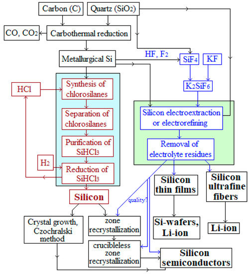
Figure 1.
Schemes for obtaining silicon.
Both methods (Siemens process and electrolysis) provide polycrystalline silicon, which can be recrystallized into a monocrystalline phase. Meanwhile, epitaxial deposits on different substrates can be obtained by electrolysis. Obtaining monocrystalline silicon is characterized by higher cost and a large volume of recycled silicon, but this silicon is slightly superior to polycrystalline silicon in terms of the efficiency of solar energy conversation. Polycrystalline silicon is cheaper, and the imperfection of its macrostructure does not prevent it from being utilized to convert solar energy. There are currently many works aimed at sensibilization of the silicon surface [24].
In the present review, a brief comparative analysis of modern methods of silicon electrodeposition is presented, and the results and prospects for the use of electrodeposited silicon in semiconductor devices, energy conversion, and storage devices are analyzed. As can be seen from the diagram in Figure 2 [25], the most popular applications of silicon remain solar energy and semiconductor materials, while the development of lithium-ion current sources with Si-based anodes has only recently gained popularity.
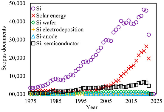
Figure 2.
Analysis of sources of scientific information on different areas of silicon use [25].
2. Molten Salts for Silicon Electrodeposition
2.1. Choice of the Molten Salt
The efficiency of silicon production by electrolysis of molten salts can be achieved with an optimal combination of electrolyte composition and electrolysis parameters. In the general case, the production of silicon by electrolysis of molten salts involves several operations, including purification of the initial reagents from impurities, electrodeposition, and separation of the silicon deposits from salt residues. The parameters of these operations affect the composition and morphology of silicon deposits, as well as the efficiency of the process as a whole. In this regard, the following factors should be taken into account when choosing molten salt and electrolysis parameters:
- -
- purity and low chemical activity of salts in relation to the materials of the electrolyzer, and the possibility of their purification;
- -
- stability of the concentration and composition of silicon-containing electroactive ions, which can be ensured by the high complexing ability of silicon ions;
- -
- stability of elemental silicon in melts with Si4+ ions;
- -
- rate of silicon electrodeposition, provided by a consistently high concentration of electroactive silicon ions, in consideration of the laws of their electroreduction;
- -
- high solubility of salts in aqueous solutions or high vapor pressure of salts during high-temperature distillation.
Simultaneous observance of all these factors is practically impossible, and as a result the effectiveness of the use of certain compositions of molten salts must be tested empirically.
2.2. Basics of the Silicon Electrodeposition
In the available works, attention was mainly focused only on the study of the kinetics of the electroreduction of silicon-containing electroactive ions, as well as on determining the parameters of silicon electrodeposition with an expected morphology. Silicon electrodeposition includes the electroreduction of silicon-containing ions at the cathode in one or more electrode steps, depending on the melt composition and electrolysis parameters according to the overall reaction (1):
Si4+ + 4e = Si0
The presence of a side reaction of disproportionation in melts has been reported (2):
Si0 + Si4+ = 2Si2+
Reaction (2) leads to a decrease in the cathodic current efficiency and a change in the kinetic parameters of silicon electrodeposition. To date, the regularities of silicon electrodeposition have been well studied, and the fundamental possibility of production of silicon with controlled morphology has been reported by varying such parameters as current density, cathode potential, melt composition, and electrolysis mode (pulse, reverse, etc.). Despite the positive results, that work has not been brought to practical implementation. Comparatively neglected issues include the cathodic current efficiency of silicon, the influence of the semiconductor nature of silicon, silicon purity, and methods of post-treatment.
2.3. Results of the Silicon Electrodeposition
To date, the greatest attention has been paid to the targeted production of silicon for energy conversion and storage devices, mainly from molten CaCl2–(NaCl)–CaO–SiO2 (CaSiO3) [26,27,28] and KF–KCl–K2SiF6 [29,30,31] with operating temperatures of 800–860 and 700–750 °C, respectively (see Table 1). The disadvantages of chloride–oxide melt are its relatively high temperature, low rates of silicon electrodeposition, and the presence of oxides in the melt. The oxides are inevitably included in the pores of the deposit, and probably degrade the performance characteristics of silicon when used in semiconductor devices, energy conversion, or storage devices. In turn, the disadvantage of the fluoride–chloride system is its relatively high chemical activity, which leads to corrosion of the structural materials of the reactor and complicates the production of high-purity silicon. Despite disadvantages, researchers [26,27,28,29,30,31] have reported silicon deposits obtained by electrolysis of CaCl2–CaO and KF–KCl-based melts in the form of fibers (from 30 to 500 nm), dendrites, thin films, and other morphologies. The declared purity of electrolytically obtained silicon reaches 99.99 wt% or more if the impurities of the electrolyte components are not taken into account [28].

Table 1.
Parameters and results of silicon electrodeposition from molten salts.
We carried out a series of experiments on silicon electrodeposition from low-fluoride systems based on mixtures of KCl, CsCl, and LiCl with additions of K2SiF6 and SiO2 in the temperature range 350 to 790 °C [32,33,34,35,36]. Due to the possibility of deep purification of chlorides by zone recrystallization [37], the proposed systems are suitable for use to obtain high-purity silicon. The disadvantage of low-fluoride systems is the lower complexing capacity of silicon, which can be improved by increasing the proportion of CsCl in the melt. As a result, we also obtained silicon deposits in the form of thin (1–5 μm) films, as well as submicron (50 to 300 nm diameter) fibers, filaments, and tubes.
The continuous appearance of new works devoted to the development of methods for producing silicon and silicon-based materials indicates the presence of shortcomings in the existing methods and the relevance of searching for new energy-efficient and resource-saving methods for producing silicon. In particular, these concerns relate to works aimed at the synthesis of silicon from iodide melts [38,39], organic electrolytes, and ionic liquids [16,17,40].
Table 1 shows the parameters and typical results of silicon electrodeposition from molten salts. As noted in Figure 1, ultrafine silicon fibers are of interest for the development of lithium-ion current sources, while thin silicon films are required for solar energy conversion and for current sources. The most representative results of the use of electrodeposited silicon from these melts are summarized in the following sections. Table 1 shows only the results of studying the obtained silicon by SEM (sizes, morphology), although XRD (lattice parameters) and ICP MS (elemental composition) methods can also be used for this purpose. Less commonly used methods are TEM (sizes), XPS (energy characteristics of Si-Si bonds), Raman spectroscopy (characteristics of Si-Si bonds), nuclear microanalysis (micro-impurities, isotopes), etc.
3. Electrolytic Silicon for Microelectronics
The first proposals for obtaining silicon by electrolytic methods were presented in terms of its use in semiconductor materials and microelectronics. However, at present there are no targeted works describing a full cycle of research on the production of silicon and its application in semiconductor materials, although a number of works have made statements about the possibility of electrodeposition of silicon of the n-, p-, or mixed p-n-type [26]. In the current author’s opinion, the absence of such works is caused by the complexity of the experimental choice for the operation to attain additional purification of silicon from impurities and electrolyte residues.
4. Electrolytic Silicon for Lithium-Ion Current Sources
The operability of a lithium-ion current source with silicon-based anodes can be ensured by using silicon with a developed surface, as well as by thin silicon films [41].
During electrolysis of a CaCl2–CaO–SiO2 melt, nanosized fibers, particles, wires, and tubes were obtained on a nickel cathode, depending on the electrolysis potential, at a cathode current density of 80–100 mA cm−2 [4]. The obtained silicon tubes had the highest specific surface area (99.9 m2 g−1) and the best lithiation–delithiation characteristics (specific capacity after 1000 cycles: 3044 mAh g−1 at a current of 0.2 A g−1, and 1033 mAh g−1 at 1 A g−1). Other studies have also reported the production of nanosized silicon deposits with discharge capacity from 500 to 3500 mAh g−1, depending on their morphology and purity.
The results of tests involving a lithium-ion current source of silicon electrodeposited from KF–KCl–K2SiF6-based melts are extremely limited. In particular, nanosized silicon particles (25–50 nm) and fibers (diameter 150–250 nm, length 1–4 μm) with a specific surface area of 14–15 m2 g−1 were obtained [31] at a temperature of 700°C and a cathode current density of 10–20 mA cm−2. The principal possibility of lithiation or delithiation of the obtained silicon was demonstrated.
As a result of the electrolysis of KCl–K2SiF6, KCl–K2SiF6–SiO2, KCl–CsCl–K2SiF6, and LiCl–KCl–CsCl–K2SiF6 melts, we obtained silicon deposits of various morphologies by varying the electrolysis parameters [32,33,34,35,36]. In particular, at a cathode current density of 20 to 150 mA cm−2, silicon fibers (diameter 100–700 nm), tubes, and needles (diameter 100–400 nm) were obtained, the specific capacity of which after 15 cycles varied from 200 to 850 mAh g−1.
Along with pure silicon, Si/C mixtures and composites [42,43], which can also be obtained by electrolysis of molten salts, are considered promising anode materials for lithium-ion current sources.
In general, a significant improvement in the energy characteristics of lithium-ion current sources can be obtained by replacing graphite anodes with silicon-basic ones. However, certain important technical issues remain unresolved, and it is necessary to address these in order for such anodes to have practical implementation.
5. Electrolytic Silicon in Solar Cells
The most demanded photoconverters are continuous silicon films with a thickness of 10–20 μm and a given content of donor micro-impurities.
In [5], the effects were studied of substrate material (Ag, Mo, C), electrodeposition potential, and particle size distribution of SiO2 on the morphology of silicon deposits obtained by electrolysis of a CaCl2–CaO–SiO2 melt at a temperature of 855 °C. A continuous photosensitive silicon film 180 μm thick was obtained on graphite at the lowest cathodic overvoltage. The authors noted the need for periodic purification of the melt from unwanted impurities, by purification electrolysis.
In [44], under conditions of potentiostatic electrolysis of a CaCl2–CaO–SiO2 melt at 850 °C, silicon films 20–25 µm thick were obtained with p-, n-, and mixed p-n-conductivity. The photosensitivity of the obtained silicon films was demonstrated as being 3.1% more effective than commercial analogues. The same authors obtained silicon films from 10 to 60 μm thick, with n-conductivity, by electrolysis of a KCl–KF–K2SiF6 melt on graphite at a temperature of 650 °C. To increase the number of electrocrystallization centers, 0.020–0.035 wt% tin was added to the melt [45]. In the opinion of the authors, the presence of up to 0.35 wt% tin in the obtained silicon films should not affect their photosensitivity, which was up to 55% of commercial samples.
In [46], the effects of cathode current density, substrate material, source (K2SiF6, SiCl4), and silicon ion concentration in the KF–KCl melt on the morphology of electrolytic silicon deposits were studied for a temperature of 750 °C. The optimal conditions for obtaining smoothed silicon films with a thickness of 20 to 60 μm were determined and their photosensitivity were demonstrated.
Several works have noted the possibility of obtaining continuous silicon films with purity of 99.9–99.99 wt%, doped with impurities such as B, Al, etc. We also carried out preliminary studies that showed the possibility of electrodeposition of photosensitive silicon films with a thickness of 1 µm, during electrolysis of LiCl–KCl–CsCl–K2SiF6 melts [36].
6. Conclusions
It follows from the above analysis that silicon electrodeposition is primarily of interest for the creation of new energy-conversion and storage devices with improved performance. Less attention has been paid to the electrodeposition of silicon to meet the requirements of microelectronics.
The most actively studied methods of silicon electrodeposition include the electrolysis of CaCl2–(NaCl)–CaO–SiO2 (CaSiO3) and KF–KCl–K2SiF6 melts with operating temperatures of 800–860 and 700–750 °C. Silicon deposits of various sizes and morphologies have been obtained, the possibility of doping silicon with micro impurities for use in energy conversion and storage devices has been shown. Alongside this, an active search is underway for new methods for the electrodeposition of silicon and silicon-based materials from molten salts, ionic liquids, and organic electrolytes.
For the practical implementation of the developed methods of silicon electrodeposition, as well as for the creation of new materials and devices for energy distribution and microelectronics, it is necessary to address more actively the issues related to the purification of electrodeposited silicon from electrolyte residues, and directly to consider the design of silicon-based materials and devices.
Funding
This work was carried out in the frame of the State Assignment number 075-03-2022-011 dated 14.01.2022 (the theme number FEUZ-2020-0037).
Institutional Review Board Statement
Not applicable.
Informed Consent Statement
Not applicable.
Data Availability Statement
Not applicable.
Conflicts of Interest
The authors declare no conflict of interest.
References
- Bhalothia, D.; Hsiung, W.; Yang, S.; Yan, C.; Chen, P.; Lin, T.; Wu, S.; Chen, P.; Wang, K.; Lin, M.; et al. Submillisecond Laser Annealing Induced Surface and Subsurface Restructuring of Cu–Ni–Pd Trimetallic Nanocatalyst Promotes Thermal CO2 Reduction. ACS Appl. Energy Mater. 2021, 4, 14043–14058. [Google Scholar] [CrossRef]
- Yu, J.; Zhang, H.; Olsson, E.; Yu, T.; Liu, Z.; Zhang, S.; Huang, X.; Li, W.; Cai, Q. A Novel Amorphous P4SSe2 Compound as an Advanced Anode for Sodium-Ion Batteries in Ether-Based Electrolytes. J. Mater. Chem. A 2021, 9, 12019–12028. [Google Scholar] [CrossRef]
- Huang, T.; Bhalothia, D.; Dai, S.; Yan, C.; Wang, K.; Chen, T. Bifunctional Pt–SnOx Nanorods for Enhanced Oxygen Reduction and Hydrogen Evolution Reactions. Sustain. Energy Fuels 2021, 5, 2960–2971. [Google Scholar] [CrossRef]
- Wang, F.; Li, P.; Li, W.; Wang, D. Electrochemical Synthesis of Multidimensional Nanostructured Silicon as a Negative Electrode Material for Lithium-Ion Battery. ACS Nano 2022, 16, 7689–7700. [Google Scholar] [CrossRef]
- Islam, M.M.; Said, H.; Hamzaoui, A.H.; Mnif, A.; Sakurai, T.; Fukata, N.; Akimoto, K. Study of Structural and Optical Properties of Electrodeposited Silicon Films on Graphite Substrates. Nanomaterials 2022, 12, 363. [Google Scholar] [CrossRef]
- Kulova, T.L. New Electrode Materials for Lithium–Ion Batteries (Review). Russ. J. Electrochem. 2013, 49, 1–25. [Google Scholar] [CrossRef]
- Gavrilin, I.M.; Grevtsov, N.L.; Pavlikov, A.V.; Dronov, A.A.; Chubenko, E.B.; Bondarenko, V.P.; Gavrilov, S.A. A New Approach for Producing of Film Structures Based on Si1−xGex. Mater. Lett. 2022, 313, 131802. [Google Scholar] [CrossRef]
- Anfimov, I.M.; Kobeleva, S.P.; Malinkovich, M.D.; Shchemerov, I.V.; Toporova, O.V.; Parkhomenko, Y.N. Mechanisms of Electroconductivity in Silicon–Carbon Nanocomposites with Nanosized Tungsten Inclusions within a Temperature Range of 20–200 °C. Russ. Microelectron. 2013, 42, 488–491. [Google Scholar] [CrossRef]
- O'Mara, W.C.; Haber, R.B.; Hunt, L.P. Handbook of Semiconductor Silicon Technology; Noyes Publications: Park Ridge, NJ, USA, 1990; ISBN 9780815517702. [Google Scholar]
- Malyshev, V.V.; Kushkhov, H.B.; Shapoval, V.I. High-Temperature Electrochemical Synthesis of Carbides, Silicides and Borides of VI-Group Metals in Ionic Melts. J. Appl. Electrochem. 2002, 32, 573–579. [Google Scholar] [CrossRef]
- Medjahed, S.; Kheloufi, A.; Bobocioiu, E.; Kefaifi, A.; Kerkar, F.; Lebbou, K. Quartz Ore Beneficiation by Reverse Flotation for Silicon Production. Silicon 2022, 14, 87–97. [Google Scholar] [CrossRef]
- Wu, J.J.; Chen, Z.; Ma, W.; Dai, Y. Thermodynamic Estimation of Silicon Tetrachloride to Trichlorosilane by a Low Temperature Hydrogenation Technique. Silicon 2017, 9, 69–75. [Google Scholar] [CrossRef]
- Cohen, U. Some Prospective Applications of Silicon Electrodeposition from Molten Fluorides to Solar Cell Fabrication. J. Electron. Mater. 1977, 6, 607–643. [Google Scholar] [CrossRef]
- Rao, G.M.; Elwell, D.; Feigelson, R.S. Electrodeposition of silicon onto graphite. J. Electrochem. Soc. 1981, 128, 1708–1711. [Google Scholar] [CrossRef]
- Bieber, A.L.; Massot, L.; Gibilaro, M.; Cassayre, L.; Taxil, P.; Chamelot, P. Silicon Electrodeposition in Molten Fluorides. Electrochim. Acta 2012, 62, 282–289. [Google Scholar] [CrossRef]
- Kuznetsova, S.V.; Dolmatov, V.S.; Kuznetsov, S.A. Voltammetric Study of Electroreduction of Silicon Complexes in a Chloride–Fluoride Melt. Russ. J. Electrochem. 2009, 45, 742–748. [Google Scholar] [CrossRef]
- Vasilév, Y.B.; Verezub, N.A.; Mezhennyi, M.V.; Prosolovich, V.S.; Prostomolotov, A.I.; Reznik, V.Y. Features of Defect Formation under the Thermal Treatment of Dislocation−Free Single−Crystal Large−Diameter Silicon Wafers with the Specified Distribution of Oxygen−Containing Gettering Centers in the Bulk. Russ. Microelectron. 2013, 42, 467–476. [Google Scholar] [CrossRef]
- Plugotarenko, N.K.; Myasoedova, T.N.; Grigoryev, M.N.; Mikhailova, T.S. Electrochemical Deposition of Silicon-Carbon Films: A Study on the Nucleation and Growth Mechanism. Nanomaterials 2019, 9, 1754. [Google Scholar] [CrossRef]
- Downes, N.; Cheek, Q.; Maldonado, S. Electroreduction of Perchlorinated Silanes for Si Electrodeposition. J. Electrochem. Soc. 2021, 168, 022503. [Google Scholar] [CrossRef]
- Walcarius, A.; Sibottier, E.; Etienne, M.; Ghanbaja, J. Electrochemically Assisted Self-Assembly of Mesoporous Silica ThinFilms. Nat. Mater. 2007, 6, 602–608. [Google Scholar] [CrossRef]
- Nguyen, N.T.; Renaud, A.; Wilmet, M.; Dumait, N.; Paofai, S.; Benjamin, D.; Whnagwui, C.; Ohashi, N.; Cordier, S.; Grasset, F.; et al. New Ultra-Violet and Near-Infrared Blocking Filters for Energy Saving Applications: Fabrication of Tantalum Metal Atom Cluster-Based Nanocomposite Thin Films by Electrophoretic Deposition. J. Mater. Chem. C 2017, 5, 10477–10484. [Google Scholar] [CrossRef]
- Sciortino, F.; Rydzek, G.; Grasset, F.; Kahn, M.L.; Hill, J.P.; Chevance, S.; Gauffre, F.; Ariga, K. Electro-Click Construction of Hybrid Nanocapsule Films with Triggered Delivery Properties. Phys. Chem. Chem. Phys. 2018, 20, 2761–2770. [Google Scholar] [CrossRef] [PubMed]
- Palma-Cando, A.; Rendón-Enríquez, I.; Tausch, M.; Scherf, U. Thin Functional Polymer Films by Electropolymerization. Nanomaterials 2019, 9, 1125. [Google Scholar] [CrossRef] [PubMed]
- Chen, W.; Truong, T.N.; Nguyen, H.T.; Samundsett, C.; Phang, S.P.; MacDonald, D.; Cuevas, A.; Zhou, L.; Wan, Y.; Yan, D. Influence of PECVD Deposition Temperature on Phosphorus Doped Poly-Silicon Passivating Contacts. Solar Energy Mater. Sol. Cells 2020, 206, 110348. [Google Scholar] [CrossRef]
- Available online: https://www.scopus.com (accessed on 15 October 2022).
- Juzeliunas, E.; Fray, D.J. Silicon Electrochemistry in Molten Salts. Chem. Rev. 2020, 120, 1690–1709. [Google Scholar] [CrossRef] [PubMed]
- Dong, Y.; Slade, T.; Stolt, M.J.; Li, L.; Girard, S.N.; Mai, L.; Jin, S. Low-Temperature Molten-Salt Production of Silicon Nanowires by the Electrochemical Reduction of CaSiO3. Angew. Chem. 2017, 129, 14645–14649. [Google Scholar] [CrossRef]
- Zou, X.; Ji, L.; Yang, X.; Lim, T.; Yu, E.T.; Bard, A.J. Electrochemical Formation of a p−n Junction on Thin Film Silicon Deposited in Molten Salt. J. Amer. Chem. Soc. 2017, 139, 16060–16063. [Google Scholar] [CrossRef] [PubMed]
- Yasuda, K.; Maeda, K.; Hagiwara, R.; Homma, T.; Nohira, T. Silicon Electrodeposition in a Water-Soluble KF–KCl Molten Salt: Utilization of SiCl4 as Si Source. J. Electrochem. Soc. 2017, 164, D67–D71. [Google Scholar] [CrossRef]
- Zaykov, Y.P.; Zhuk, S.I.; Isakov, A.V.; Grishenkova, O.V.; Isaev, V.A. Electrochemical Nucleation and Growth of Silicon in the KF–KCl–K2SiF6 Melt. J. Solid State Electrochem. 2015, 19, 1341–1345. [Google Scholar] [CrossRef]
- Chemezov, O.V.; Isakov, A.V.; Apisarov, A.P.; Brezhestovsky, M.S.; Bushkova, O.V.; Batalov, N.N.; Zaikov, Y.P.; Shashkin, A.P. Electrolytic Production of Silicon Nanofibers from the KCl–KF–K2SiF6–SiO2 Melt for Composite Anodes of Lithium-Ion Batteries. Electrochim. Energetics 2013, 13, 201–204. [Google Scholar] [CrossRef]
- Ustinova, Y.; Pavlenko, O.; Gevel, T.; Zhuk, S.; Suzdaltsev, A.; Zaikov, Y. Electrodeposition of Silicon from the Low-Melting LiCl–KCl–CsCl–K2SiF6 Electrolytes. J. Electrochem. Soc. 2022, 169, 032506. [Google Scholar] [CrossRef]
- Gevel, T.; Zhuk, S.; Leonova, N.; Leonova, A.; Trofimov, A.; Suzdaltsev, A.; Zaikov, Y. Electrochemical Synthesis of Nano-Sized Silicon from KCl–K2SiF6 Melts for Powerful Lithium-Ion Batteries. Appl. Sci. 2021, 11, 10927. [Google Scholar] [CrossRef]
- Trofimov, A.A.; Leonova, A.M.; Leonova, N.M.; Gevel, T.A. Electrodeposition of Silicon from Molten KCl–K2SiF6 for Lithium-Ion Batteries. J. Electrochem. Soc. 2022, 169, 020537. [Google Scholar] [CrossRef]
- Gevel, T.A.; Zhuk, S.I.; Leonova, N.M.; Leonova, A.M.; Suzdaltsev, A.V.; Zaikov, Y.P. Electrodeposition of Silicon from the KCl–CsCl–K2SiF6 Melt. Russ. Met. (Metally) 2022, 2022, 958–964. [Google Scholar] [CrossRef]
- Pavlenko, O.B.; Ustinova, Y.A.; Zhuk, S.I.; Suzdaltsev, A.V.; Zaikov, Y.P. Silicon Electrodeposition from Low-Melting LiCl-KCl-CsCl Melts. Russ. Met. (Metally) 2022, 2022, 818–824. [Google Scholar] [CrossRef]
- Nikolaev, A.Y.; Mullabaev, A.R.; Suzdaltsev, A.V.; Kovrov, V.A.; Kholkina, A.S.; Shishkin, V.Y.; Zaikov, Y.P. Purification of Alkali-Metal Chlorides by Zone Recrystallization for the Use in Pyrochemical Processing of Spent Nuclear Fuel. Atomic Energy 2022, 131, 195–201. [Google Scholar] [CrossRef]
- Laptev, M.V.; Isakov, A.V.; Grishenkova, O.V.; Vorob'ev, A.S.; Khudorozhkova, A.O.; Akashev, L.A.; Zaikov, Y.P. Electrodeposition of Thin Silicon Films from the KF–KCl–KI–K2SiF6 Melt. J. Electrochem. Soc. 2020, 167, 042506. [Google Scholar] [CrossRef]
- Laptev, M.V.; Khudorozhkova, A.O.; Isakov, A.V.; Grishenkova, O.V.; Zhuk, S.I.; Zaikov, Y.P. Electrodeposition of Aluminum-Doped Thin Silicon Films from a KF–KCl–KI–K2SiF6–AlF3 Melt. J. Serb. Chem. Soc. 2021, 86, 1075–1087. [Google Scholar] [CrossRef]
- Chen, X.; Gerasopoulos, K.; Guo, J.; Brown, A.; Wang, C.; Ghodssi, R.; Culver, J.N. A Patterned 3D Silicon Anode Fabricated by Electrodeposition on a Virus-Structured Current Collector. Adv. Funct. Mater. 2011, 21, 380–387. [Google Scholar] [CrossRef]
- Galashev, A.Y.; Suzdaltsev, A.V.; Ivanichkina, K.A. Design of the High Performance Microbattery with Silicene Anode. Mater. Sci. Eng. B 2020, 261, 114718. [Google Scholar] [CrossRef]
- Salah, M.; Hall, C.; Murphy, P.; Francis, C.; Kerr, R.; Stoehr, B.; Rudd, S.; Fabretto, M. Doped and Reactive Silicon Thin Film Anodes for Lithium Ion Batteries: A review. J. Power Sources 2021, 506, 230194. [Google Scholar] [CrossRef]
- Hou, Y.; Yang, Y.; Meng, W.; Lei, B.; Ren, M.; Yang, X.; Wang, Y.; Zhao, D. Core-Shell Structured Si@Cu Nanoparticles Encapsulated in Carbon Cages as High-Performance Lithium-Ion Battery Anodes. J. Alloys Compd. 2021, 874, 159988. [Google Scholar] [CrossRef]
- Zou, X.; Ji, L.; Ge, J.; Sadoway, D.R.; Yu, E.T.; Bard, A.J. Electrodeposition of Crystalline Silicon Films from Silicon Dioxide for Low-Cost Photovoltaic Applications. Nat. Commun. 2019, 10, 5772. [Google Scholar] [CrossRef] [PubMed]
- Peng, J.; Yin, H.; Zhao, J.; Yang, X.; Bard, A.J.; Sadoway, D.R. Liquid-Tin-Assisted Molten Salt Electrodeposition of Photoresponsive n-Type Silicon Films. Adv. Funct. Mater. 2018, 28, 1703551. [Google Scholar] [CrossRef]
- Yasuda, K.; Kato, T.; Norikawa, Y.; Nohira, T. Silicon Electrodeposition in a Water-Soluble KF–KCl Molten Salt: Properties of Si Films on Graphite Substrates. J. Electrochem. Soc. 2021, 168, 112502. [Google Scholar] [CrossRef]


Publisher’s Note: MDPI stays neutral with regard to jurisdictional claims in published maps and institutional affiliations. |
© 2022 by the author. Licensee MDPI, Basel, Switzerland. This article is an open access article distributed under the terms and conditions of the Creative Commons Attribution (CC BY) license (https://creativecommons.org/licenses/by/4.0/).