Article

Solution-Processable and Eco-Friendly Functionalization of Conductive Silver Nanoparticles Inks for Printable Electronics

1
Centro de Investigaciones en Dispositivos Semiconductores, Instituto de Ciencias, Benemérita Universidad Autónoma de Puebla, Puebla 72570, Mexico
2
Institut National de la Recherche Scientifique, Varennes, QC J3X 1P7, Canada
*
Author to whom correspondence should be addressed.
Electron. Mater. 2024, 5(2), 45-55; https://doi.org/10.3390/electronicmat5020004
Submission received: 23 February 2024 / Revised: 27 March 2024 / Accepted: 12 April 2024 / Published: 16 April 2024

Abstract

:
The functionalization of conductive inks has been carried out through the decomposition of hydrogen peroxide (H2O2) onto the surface of silver nanoparticles (AgNPs). The ink prepared using this eco-friendly chemical reagent has been characterized structurally, chemically, and morphologically, showing the presence of stable AgNPs with suitable properties as well as the absence of residual contamination. The electrical conductivity of such a solution-processable ink is evidenced for patterns designed on flexible photographic paper substrates, using a refillable fountain pen that is implemented as a printing mechanism for the fabrication of simple printed circuit boards (PCBs). The functionality and durability of the tested systems are demonstrated under various mechanical constraints, aiming to basically reproduce the normal operation conditions of flexible electronic devices. The obtained results indicate that the implementation of these AgNP-based inks is relevant for direct applications in inkjet printing technology, thus paving the way for the use of greener chemicals in ink preparation.

1. Introduction

Printed electronics (PE) is a low-cost fabrication technique with a small environmental footprint that is suitable for large-scale applications [1,2]. It can be implemented to fabricate a great variety of electronic devices, including flexible hybrid electronic systems, which usually integrate circuits from both the silicon technology and the flexible printing technology [3,4,5]. These active components can be achieved on paper, polyethylene terephthalate (PET), and other types of commonly used flexible and eco-friendly substrates [6]. Printable electronics involves the efficient deposition of liquid solutions containing various nanomaterials, such as conductive silver nanoparticles (AgNPs), which provide them with specific functions. The obtained compounds can then be mixed with a great variety of natural and synthetic polymers to manufacture electronic devices at a low cost. Functional systems are achieved through the design of various patterns aiming to achieve electrical current conduction or the activation of various physico-chemical processes, such as those involved in energy conversion, harvesting, or storage [7,8,9]. The implementation of this technology can be achieved using affordable and multifunctional commercial writing tools, such as a fountain pen, a ballpoint pen, or a marker pen [10,11]. Ultimately, the synthesis of such liquid compounds aims at their implementation in ink-jet printing, which requires that the inks are subject to very strict conditions regarding their viscosity, wettability, and solubility [2].
The ink formulation is chosen according to its drying time, versatility in large-scale production, stability, and environmental impact. An important factor that influences these properties is related to the system solubility, which requires the use of organic solvents or the development of water-based ink [1,12]. AgNP-based inks are especially advantageous and more environmentally friendly because the particles are dispersed at high concentrations in a non-pollutant reagent, such as water or hydrogen peroxide (H2O2), which reduces waste production. The use of an H2O2 water mixture as an eco-friendly alternative prevents the formation of volatile organic compounds (VOCs) and is less harmful for human health [1,12] since its decomposition produces only water and oxygen. H2O2 has also been found to be suitable for synthesizing high-purity Ag crystals [13,14], where its ability to form free radicals increases the catalytic properties of the medium and results in the stronger solubility of AgNPs [15,16]. In addition, H2O2 is compatible with many industrial processes, as it is already implemented in the electronics industry to clean germanium and silicon semiconductor wafers, as well as to etch printed circuit boards [13]. H2O2 is less detrimental to the electrical conductivity of the sample compared to other humectants, surfactants, and binders, such as alcohols, glycols, and resins, which can modify the surface of the NPs, avoid their agglomeration, and affect the viscosity of the inks and the interaction between the particles [7,17]. Last but not least, as no additional sintering and/or thermal processes are needed to eliminate the organic stabilizers and their residual products, this reactant is more suitable for flexible electronics, where most of the substrates can become drastically distorted above 70 °C [1,7,18].
In this work, we report the synthesis of inks based on AgNPs mixed with a hydrogen peroxide solution and their implementation as conductive wire and circuits on a flexible substrate. Advanced characterizations are conducted to determine the structural composition and morphology of AgNPs. The electrical properties of the printed and handwritten circuits are investigated and tested under various mechanical constraints, using experimental prototypes that were achieved through the deposition of functionalized inks onto photographic paper. To check the relevance of such inks in printing technology, Ag contacts onto photographic paper and flexible hybrid conductive circuits have been achieved using the handwriting technique with a fountain pen. One of these prototypes is then exposed to various binding constraints and stresses in order to evaluate its mechanical resistance under basic operating conditions. The retention of both the structural integrity and the functionality of the tested conductive device is found to be suitable for the implementation of AgNP-based inks processed with H2O2 in wearable and flexible electronics.

2. Materials and Methods

2.1. Materials Synthesis Methods

Conductive AgNPs were synthesized through the chemical reduction of 0.03 M C6H5Na3O7 (99.0% Sigma-Aldrich, St. Louis, MO, USA), 0.05 M NaBH4 (99.0% Sigma-Aldrich), and 0.15 M AgNO3 (99.0% Sigma-Aldrich) within an ice bath. The AgNPs were washed with EtOH (Sigma-Aldrich) and centrifuged to remove excess solvents and residues. The obtained product was then mixed with a commercial H2O2 solution at 3% using a total volume of 5 mL to dissolve the AgNPs (20 wt. %), and then it was sonicated for 3 h. A color change from gray to black is observed in this colloidal solution during this step, leading to ink preparation. To test the performance of this AgNP-based ink, the solution was then deposited onto a silicon substrate or photographic paper. Finally, with a generic extrafine point fountain pen of 0.6 mm diameter refilled with 1 mL of AgNP-based ink, a drawing of a basic circuit pattern was realized, and it was then dried at room temperature to observe whether the electrical behavior would turn on an LED.

2.2. Characterization

The crystalline structure of the materials was determined using a Discover X-ray diffractometer (Bruker D8 Advance, Billerica, MA, USA), operated with the Cu-kα radiation source to perform θ–2θ diffraction measurements between 20 and 90°. The microscopic investigations were carried out with a Tescan Vega3 LMH scanning electron microscope (SEM), as well as a Park Systems (XE-150) atomic force microscope (AFM). The size, polydispersity index (PDI), and zeta potential of the AgNP-based ink were measured with a Zetasizer Nano-ZS90 instrument. Electrical measurements were performed using a Keithley-4200 Semiconductor Characterization System at room temperature (RT) under ambient air conditions.

3. Results and Discussion

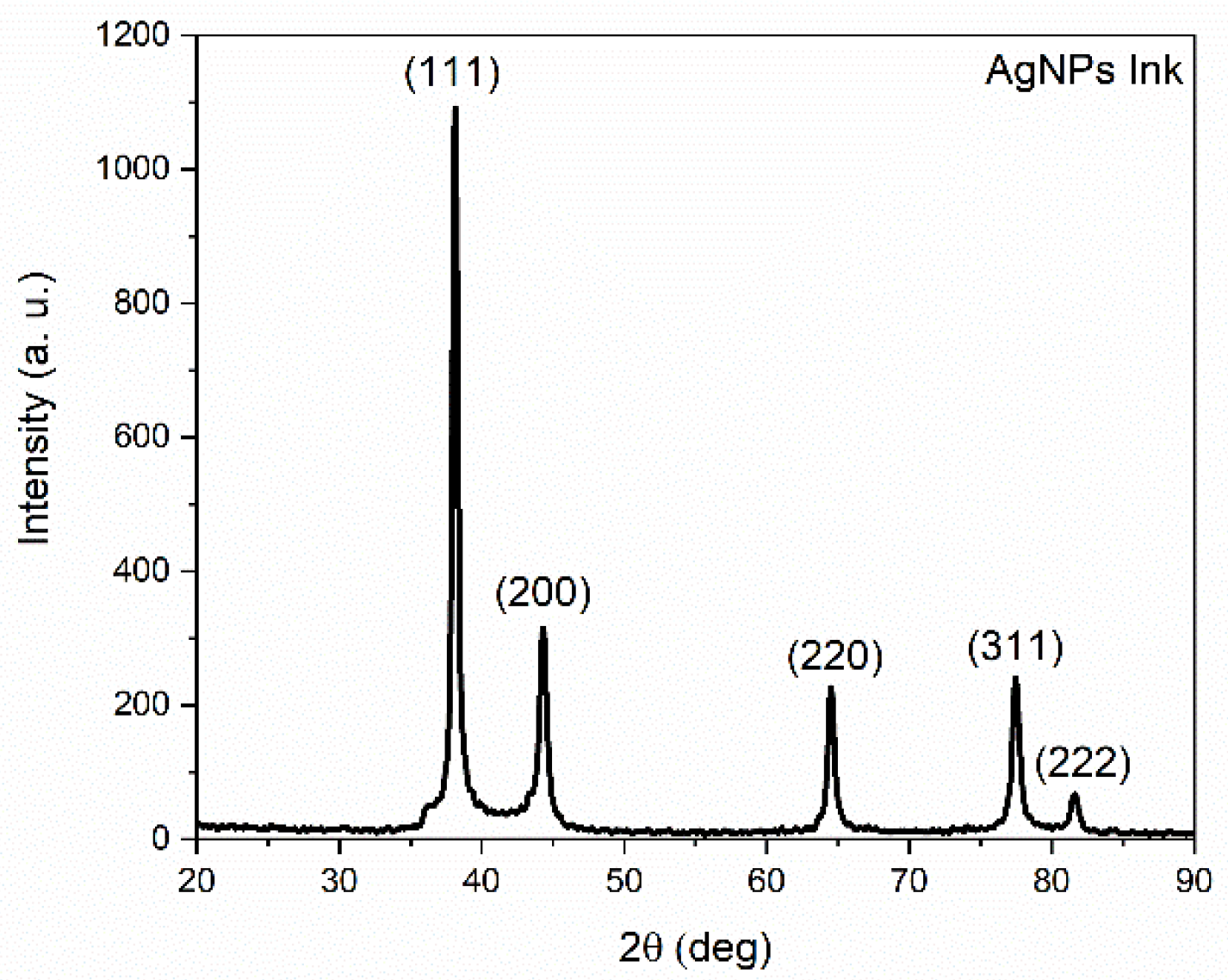
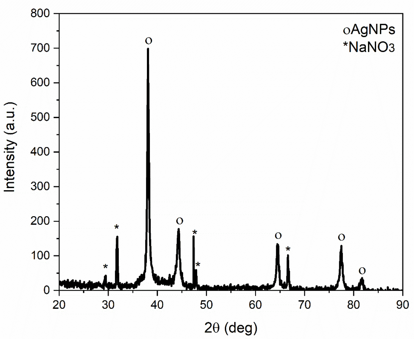
3.1. XRD Measurements

The X-ray diffraction (XRD) pattern of the synthesized AgNPs is shown in Figure 1. Their FCC structure is identified in JCPDS 00-004-0783 [19]. This measurement shows the presence of intense peaks at 38°, 44°, 64°, 77°, and 81°, related to XRD onto the crystalline planes of (111), (200), (220), (311), and (222) orientations, respectively. The presence of NaNO3 is also detected (JCPDS 00-036-1474) [19] as a secondary product resulting from AgNP synthesis [20,21]. This compound may be present as a precipitate before mixing with H2O2. After mixing, only the diffraction peaks of Ag are observed in Figure 2, which means that most of NaNO3 has been removed without requiring any additional purification process [14]. Such a feature indicates that H2O2 acts as a reducing agent during AgNP-based ink preparation [14,22]. The different noise contributions to the data reported in Figure 1 and Figure 2 resulted from the use of different acquisition times. It is also noteworthy that for both samples, no silver oxide was detected. This point will be discussed in more detail in the next section, related to their SEM/EDS analyses.
According to references [23,24,25], the chemical reactions of H2O2 can be described as follows:
The electron transfers resulting from the dissociation of H2O2 promote the adhesion of OH¯ onto the outer surface of AgNPs, generating Ag+, hydroxyl radicals, and superoxide anions, according to the reactions (1) and (2) [23].
AgNP + H2O2 → Ag+ + HO· + OH¯
HO· + OH¯ + H2O2 → O2¯ + 2H2O
The superoxide anion then transfers electrons to the AgNPs, which results in the formation of highly reactively charged NPs (Ag*¯), inducing the reduction of oxygen and leading to the regeneration of AgNPs, according to (3) and (4), respectively [24,25].
Ag+ + O2¯ → AgNP*¯ + O2
Ag+ + AgNP*¯ → AgNP + AgNP
The pH of AgNP-based ink is measured to be 7 after preparation, which could appear as quite a low value for a compound mixed with H2O2. As no acidic or basic reagents have been added to the solution, this neutral pH indicates that all H2O2 efficiently reacted with Ag. Such a feature also does not exclude that the AgNP-based ink contains a small fraction of Ag in excess.

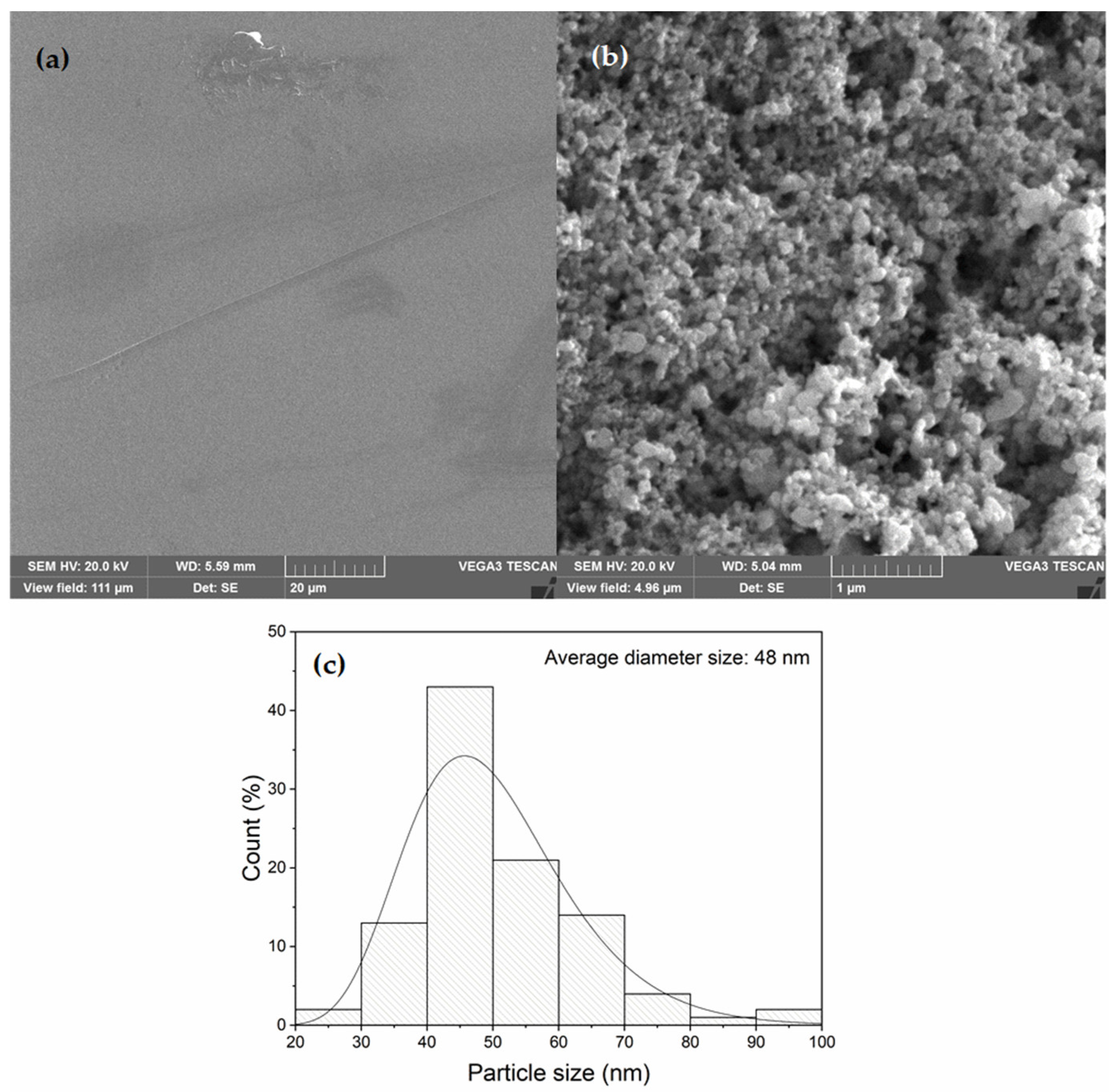
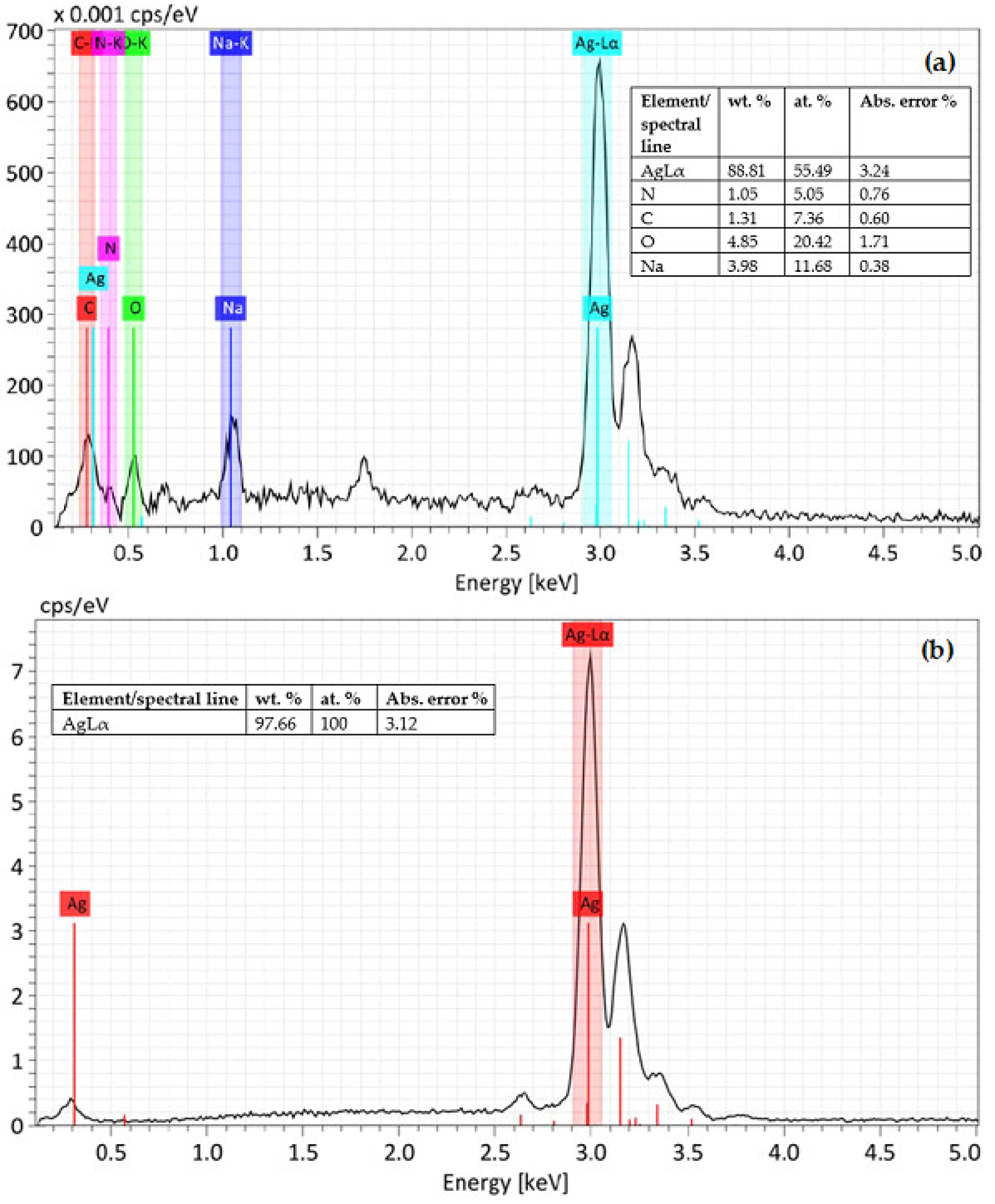
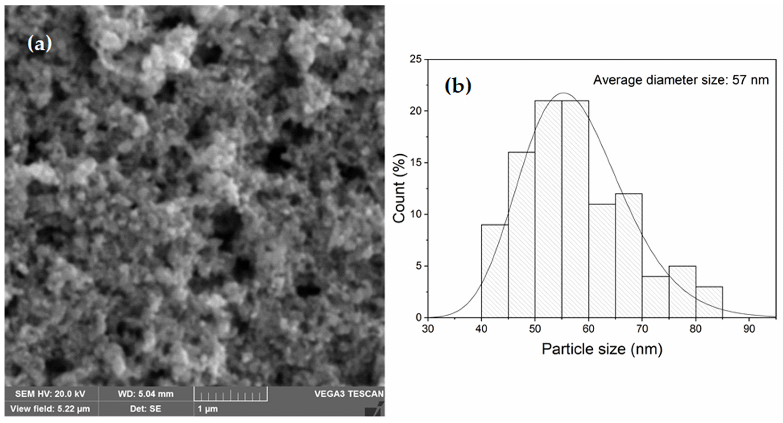
3.2. SEM/EDS Analysis

The investigations by SEM are presented in Figure 3. Figure 3a shows the surface of the clean photographic paper before the ink deposition, while Figure 3b shows the sample surface obtained after deposition, followed by a drying time of 15 min at RT. For the latter, the ink film results in the agglomeration of particles of a spherical shape, which is in agreement with previous studies [26]. The average diameter of the AgNPs contained in the deposited ink was estimated using ImageJ software, where more than 100 NPs were accounted for. From the SEM images, the average size of the nanoparticles is 48 ± 12 nm after fitting the AgNP size distribution histogram in Figure 3c using the standard log normal function described in the references [27,28,29]. The same approach was conducted for the particles without dispersion in H2O2; see Figure 4a, where an average size of 57 ± 10 nm is found, as computed in Figure 4b. The decrease in the average diameters of AgNPs inside the functionalized ink is attributed to sonication effects [30,31].
Investigations using energy dispersion X-ray spectroscopy (EDS) were carried out to determine the chemical composition of pure AgNPs (e.g., not mixed with H2O2) and AgNP-based ink deposited on photographic paper. The quantification of the chemical elements reported in the insets of Figure 5a indicates the presence of small concentrations of nitrogen, oxygen, and sodium in the first sample, which is in agreement with the detection of NaNO3 reported in the XRD peaks of Figure 1, as well as a small amount of carbon coming from contamination. In Figure 5b, all of these quantities are found to become negligible for EDS measurements conducted on AgNP-based ink. Although the EDS measurements usually provide only qualitative information, the intensity of the Ag signal is high, indicating a strong concentration of AgNPs as well as the absence of any other elements. Whereas the inks prepared from reagents such as polyvinylpyrrolidone (PVP), diethylene amine (DEA), ammonium hydroxide, and hydroxyethyl cellulose usually lead to undesirable chemical residues [32,33,34,35], no additional chemical or evaporation process is required to remove possible contaminants. The ink obtained after mixing AgNPs with H2O2 can be directly implemented, which simplifies its use on a large scale and eliminates the risk of deteriorating the flexible substrate where it has been deposited during post-annealing treatments.
Regarding the apparent absence of silver oxide (or its concentration, which could be lower than the detection limit of the EDS analyzer), it may be related to the redox mechanism induced by H2O2, leading to the generation of Ag+, hydroxyl radicals, and superoxide anions. According to the work of Sundaresan et al. [36], it has been suggested that the formation of symmetric or asymmetric oxide layers at the outer surface of the AgNPs strongly depends on the experimental conditions. The authors mentioned that the ionization of Ag over the whole outer surface of the AgNPs can prevent or drastically limit its oxidation. Such a scenario could also be compatible with the reduced pH of AgNP-based ink.

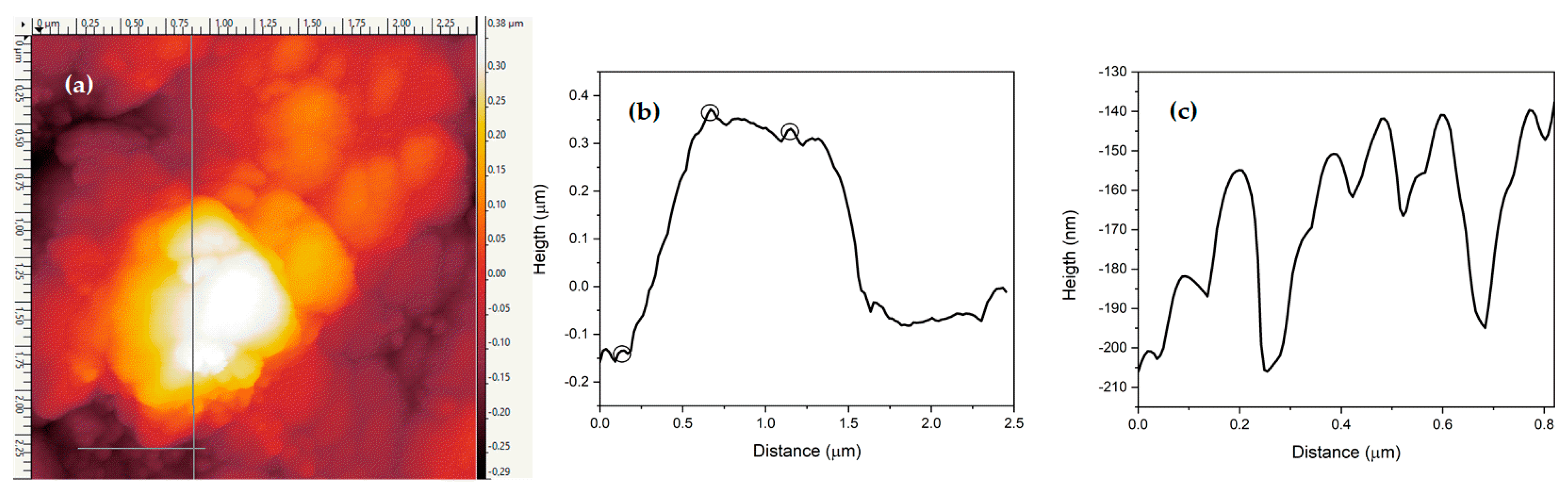
3.3. Topography Measurement by AFM

Through AFM measurements performed over an area of 2.5 µm2, the surface topography of the deposited ink was analyzed using the Gwyddion 2.62 software [37]. The deposited AgNPs reveal a sample surface with a roughness that is quite a bit greater than that of pristine photographic paper. As expected from our SEM investigation and in agreement with previous works [37,38], our results show several irregular and compact arrangements of the agglomerated AgNP-based ink over the whole sample surface. The mapped vertical and horizontal gray lines of Figure 6a scan a region of overlapped NPs. For the vertical scan, the maximum height profile is 470 nm, while the minimum height is 200 nm, as shown in Figure 6b. These particles are found to have well-defined diameters lower than 50 nm. The horizontal scan marked in Figure 6c shows the clustering of the AgNPs in a deeper region. According to the profile illustrated by the variations recorded in Figure 6c, the nanoparticles have diameters between 30 and 60 nm, which confirms both their relatively uniform spherical shape and their dimensions measured by SEM.

3.4. Dynamic Light Scattering (DLS) and Zeta Potential Analyses

The particle size, size distribution, and zeta potential were measured using the DLS technique to corroborate the SEM/AFM results and determine the stability of AgNP-based ink. The diameter of the particles was measured to be 50 nm, which is in agreement with the results presented in sections B and C.
The sample also presents a moderate size distribution according to the polydispersity index (PDI), which is found to be greater than 0.50. Values smaller than 0.05 are rarely seen other than for highly monodispersed standards, and values greater than 0.70 are highly polydispersed, according to the ISO standards 13321:1996 E and ISO 22412:2008 [39]. As reported in the AFM analysis, both the agglomeration and overlap of AgNPs may artificially increase the PDI measured by DLS, which is evaluated to be around 0.27 from our SEM analysis [40], confirming that the dispersion of the particles is in a moderate range. Finally, a negative zeta potential of −30.5 mV is measured, which denotes that the ink is stable [41,42]. Such a value is consistent with those reported between −35 mV and −25 mV for nanoparticles dispersed in water with organic additives [43,44,45].

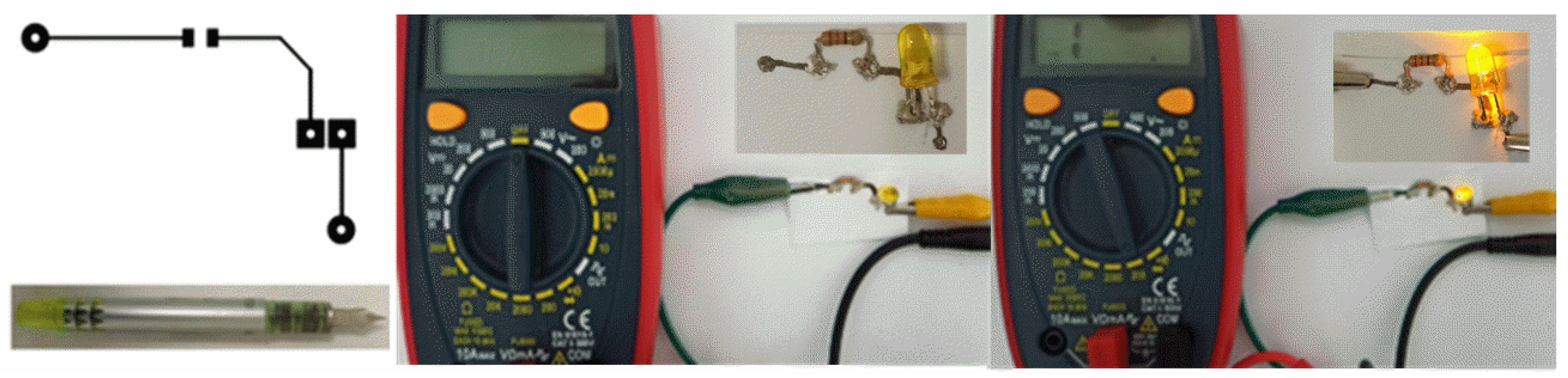
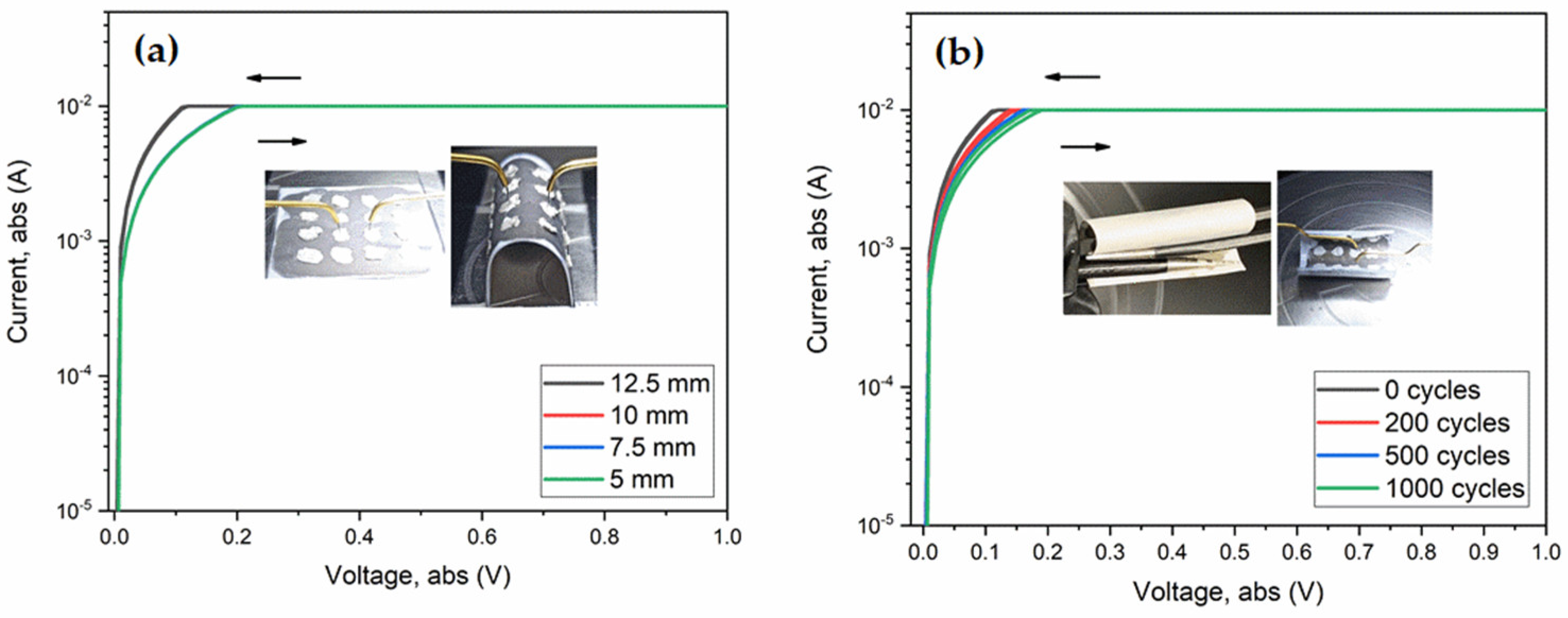
3.5. Electrical Characterization and Testing after Bending

Current-to-voltage measurements were performed with forward and reverse sweeps in order to evidence possible hysteresis effects related to material degradation and memory effects (such as charge–discharge mechanisms) after successive flexions and bending cycles. All the parameters and data recorded for this set of experiments are summarized in Table 1. A regular, symmetric, and reproducible behavior, compatible with the one expected for ohmic contacts, is shown in Figure 7. Here, the apparent saturation observed above 0.1 V results from the equipment limitation. A nominal resistance of 11.74 Ω is measured when the flexible substrate is flat, and the resistance increases up to 17.99 Ω when it is brought to a bending radius curvature of 12.5 mm, as shown in the inset of Figure 7a. After successive bending cycles, it was found that the resistance increases and stabilizes at around 20 Ω for radius curvatures decreasing from 10 mm to 5 mm. Despite the enhancement of the bending curvature, the ohmic nature, as well as the resistance of the conductive wire, were not significantly affected.
For photographic paper with a thickness of 0.2032 mm, bending at a curvature radius of 12.5 mm corresponds to a mechanical stress of ~0.8%, and the one at a curvature radius of 5 mm corresponds to a mechanical stress of 2% [46]. The low variations of the electrical resistance reported in the third column of Table 1 (with an error rate of ±5%) suggest that there is no significant change in the distance between the deposited AgNPs nor breakage in their electrical contact, thus indicating that the system remains operational under the applied mechanical constraints.
Current-to-voltage measurements obtained for bending cycles increasing from 0 to 1000 are shown in Figure 7b and reported in the fifth column of Table 1. The current measured is close to 10−2 A and remains almost constant, showing a slight decrease in the electrical resistance with respect to its nominal value (reported in the third column). As previously noted, no hysteresis effects were observed, which means that the functionality of the ink was not altered when the bending cycles increased.
Both the mechanical resistance and durability of AgNP-based ink spread onto the surface of the photographic paper make this compound a potential candidate for hybrid PCB applications. Its use in advanced manufacturing with a low environmental impact is realistic, as is its relevance for greener printing-based technologies.

3.6. Application Perspective

To illustrate an example of practical applications, AgNP-based ink was loaded inside a fountain pen and used to trace a pattern by handwriting on the photographic paper. As illustrated in the pictures presented in the inset of Figure 8, the electrical circuit achieved through this very simple method is powering an LED when connected to an external voltage source of 9 V. The LED was successively turned on and off, demonstrating efficient current conduction. Despite being a very basic demonstration of ink functionality, this kind of prototype shows the capabilities of incorporating AgNPs into liquid solutions for printing electronic components or facilitating the replacement of damaged PCB boards. These functional inks could also be implemented to achieve a great variety of flexible devices, spanning from health monitoring systems to energy converters. Both the reduced size and weight of these advanced devices make them more particularly relevant for applications in aerospace [47], packaging [48,49], health [50], and biodegradable electronics [51,52].

4. Conclusions

The preparation of conductive ink based on pure AgNPs mixed with H2O2 was successfully achieved. Although non-pollutant H2O2 has a high oxidative capacity, it does not alter the structure of Ag or the composition of NPs. The dispersion of AgNPs (20 wt. %) in a volume of H2O2 (5 mL) makes the solution electrically conductive and free of contaminants due to the presence of OH-free radicals and superoxide ions that promote successive redox reactions as well as the release of the secondary chemical products. AgNPs have an average and uniform spherical size of about 50 nm in diameter, and they agglomerate into a thin, compact layer. A strong affinity between AgNPs and the photographic paper was observed, so the sample drying was simply achieved at room temperature for 15 min without requiring any additional purification process. AgNP-based ink was implemented into a basic circuit, achieved by direct writing, to demonstrate its electrical conductivity and study how it behaves after successive bending experiments. No significant changes in the electrical conduction or hysteresis effects were reported when the number of cycles and the intensity of their flexures both increased, suggesting that the system remains operational under such mechanical constraints. This feature occurred even though the concentration of AgNPs was low compared to the concentration of the medium, which indicates that AgNP-based inks prepared using no pollutant solvent are suitable for future implementation in flexible printable electronics.

Author Contributions

Conceptualization, S.C. and M.A.D.; methodology, S.C.; validation, S.C., D.B. and M.A.D.; formal analysis, S.C., D.B. and M.A.D.; investigation, S.C.; resources, D.B. and M.A.D.; data curation, S.C.; writing—original draft preparation, S.C.; writing—review and editing, S.C., D.B., and M.D; visualization, S.C. and M.A.D.; supervision, D.B. and M.A.D.; project administration, D.B. and M.A.D.; funding acquisition, D.B. and M.A.D. All authors have read and agreed to the published version of the manuscript.

Funding

This work was supported by the Groupe de Travail Québec-Mexique 2019–2021 MRIF-SRE and the Fondo Sectorial de Investigación para la Educación CONACYT-SEP (grant number A1-S-7888).

Data Availability Statement

The original contributions presented in the study are included in the article; further inquiries can be directed to the corresponding author.

Acknowledgments

The authors would like to thank the Instituto de Física de la Universidad Autónoma de Puebla and the Institut National de la Recherche Scientifique for the characterizations performed using their research facilities, as well as the technical and scientific supports of C. Chabanier and C. Harnagea (INRS). The works conducted at INRS were supported by the NSERC Alliance and the Prima Québec programs (grant numbers 561014-2020 and R20-13-002, respectively). All the authors are also grateful to the UNESCO MATECSS chair for initiating this international collaborative work in 2018.

Conflicts of Interest

The authors declare no conflicts of interest.

References

  1. Cano-Raya, C.; Denchev, Z.Z.; Cruz, S.F.; Viana, J.C. Chemistry of solid metal-based inks and pastes for printed electronics—A review. Appl. Mater. Today 2019, 29, 416–430. [Google Scholar] [CrossRef]
  2. Liu, Y.; Zhu, H.; Xing, L.; Bu, Q.; Ren, D.; Sun, B. Recent advances in inkjet-printing technologies for flexible/wearable electronics. Nanoscale 2023, 15, 6025–6051. [Google Scholar] [CrossRef] [PubMed]
  3. Ma, Y.; Zhang, Y.; Cai, Z.; Han, Z.; Liu, X.; Wang, F.; Cao, Y.; Wang, Z.; Li, H.; Chen, Y.; et al. Flexible Hybrid Electronics for Digital Healthcare. Adv. Mater. 2019, 32, 1902062. [Google Scholar] [CrossRef] [PubMed]
  4. Schwartz, D.E. Flexible Hybrid Electronic Circuits and Systems. IEEE J. Emerg. Sel. 2017, 7, 27–37. [Google Scholar] [CrossRef]
  5. Li, Z.; Chang, S.; Khuje, S.; Ren, S. Recent Advancement of Emerging Nano Copper-Based Printable Flexible Hybrid Electronics. ACS Nano 2021, 15, 6211–6232. [Google Scholar] [CrossRef] [PubMed]
  6. Soum, V.; Lehmann, V.; Lee, H.; Khan, S.; Kwon, O.-S.; Shin, K. A Novel Polymeric Substrate with Dual-Porous Structures for High-Performance Inkjet-Printed Flexible Electronic Devices. Macromol. Mater. Eng. 2023, 308, 2300107. [Google Scholar] [CrossRef]
  7. Li, D.; Lai, W.Y.; Zhang, Y.-Z.; Huang, W. Printable Transparent Conductive Films for Flexible Electronics. Adv. Mater. 2018, 30, 17047738. [Google Scholar] [CrossRef]
  8. Zhan, N.; Huang, C.; Wan, S.; Kang, L.; Hu, M.; Zhang, Y.; Wu, X.; Zhang, J. A Novel Flexible Silver Heater Fabricated by a Solution-Based Polyimide Metalization and Inkjet-Printed Carbon Masking Technique. ACS Appl. Electron. Mater. 2019, 1, 928–935. [Google Scholar] [CrossRef]
  9. Mo, L.; Guo, Z.; Yang, L.; Zhang, Q.; Fang, Y.; Xin, Z.; Chen, Z.; Hu, K.; Han, L.; Li, L. Silver Nanoparticles Based Ink with Moderate Sintering in Flexible and Printed Electronics. Int. J. Mol. Sci. 2019, 20, 2124. [Google Scholar] [CrossRef]
  10. Arya, N.; Chandran, Y.; Singh, A.; Sharma, R.; Halder, A.; Balakrishnan, V. Substrate Versatile Roller Ball Pen Writing of Nanoporous MoS2 for Energy Storage Devices. ACS Appl. Mater. Interfaces 2023, 15, 41447–41456. [Google Scholar] [CrossRef]
  11. Ersu, G.; Sozen, Y.; Sánchez-Viso, E.; Kuriakose, S.; Juárez, B.H.; Mompean, F.J.; Garcia-Hernandez, M.; Visscher, L.; Magdaleno, A.J.; Prins, F.; et al. Pen Plotter as a Low-Cost Platform for Rapid Device Prototyping with Solution-Processable Nanomaterials. Adv. Eng. Mater. 2023, 25, 2300226. [Google Scholar] [CrossRef]
  12. Orrill, M.; Abele, D.; Wagner, M.J.; LeBlanc, S. Sterically Stabilized Multilayer Graphene Nanoshells for Inkjet Printed Resistors. Electron. Mater. 2021, 2, 394–412. [Google Scholar] [CrossRef]
  13. Campos-Martin, J.M.; Blanco-Brieva, G.; Fierro, J.L.G. Hydrogen Peroxide Synthesis: An Outlook beyond the Anthraquinone Process. Angew. Chem. Int. Ed. 2006, 45, 6962–6984. [Google Scholar] [CrossRef] [PubMed]
  14. Gatemala, H.; Ekgasit, S.; Wongravee, K. High purity silver microcrystals recovered from silver wastes by eco-friendly process using hydrogen peroxide. Chemosphere 2017, 178, 249–258. [Google Scholar] [CrossRef] [PubMed]
  15. Mypati, S.; Dhanushkodi, S.R.; McLaren, M.; Docoslis, A.; Peppley, B.A.; Barz, D.P. Optimized inkjet-printed silver nanoparticle films: Theoretical and experimental investigations. RSC Adv. 2018, 8, 19679–19689. [Google Scholar] [CrossRef]
  16. Mahy, J.G.; Kiendrebeogo, M.; Farcy, A.; Drogui, P. Enhanced Decomposition of H2O2 Using Metallic Silver Nanoparticles under UV/Visible Light for the Removal of p-Nitrophenol from Water. Catalysts 2023, 13, 842. [Google Scholar] [CrossRef]
  17. Rajan, K.; Roppolo, I.; Chiappone, A.; Bocchini, S.; Perrone, D.; Chiolerio, A. Silver nanoparticle ink technology: State of the art. Nanotechnol. Sci. Appl. 2016, 9, 1–13. [Google Scholar] [CrossRef] [PubMed]
  18. Nayak, L.; Mohanty, S.; Nayak, S.; Ramadoss, A. A review on inkjet printing of nanoparticles inks for flexible electronics. J. Mater. Chem. C. 2019, 7, 8771–8795. [Google Scholar] [CrossRef]
  19. Kabekkodu, S.N.; Faber, J.; Fawcett, T. New Powder Diffraction File (PDF-4) in relational database format: Advantages and data-mining capabilities. Acta Crystallogr. Sect. B Struct. Sci. 2002, 58, 333–337. [Google Scholar] [CrossRef]
  20. Nhugn, N.T.H.; Dat, N.T.; Thi, C.M.; Viet, P.V. Fast and simple synthesis of triangular silver nanoparticles under the assistance of light. Colloids Surf. A Physicochem. Eng. 2020, 594, 124659. [Google Scholar] [CrossRef]
  21. Adio, S.O.; Rana, A.; Chanabsha, B.; BoAli, A.A.K.; Essa, M.; Alsaadi, A. Silver Nanoparticle-Loaded Activated Carbon as an Adsorbent for the Removal of Mercury from Arabian Gas-Condensate. Arab. J. Sci. Eng. 2019, 44, 6285–6293. [Google Scholar] [CrossRef]
  22. Parnklang, T.; Lamlua, B.; Gatemala, H.; Thammacharoen, C.; Kuimalee, S.; Lohwongwatana, B. Shape transformation of silver nanospheres to silver nanoplates induced by redox reaction of hydrogen peroxide. Mater. Chem. Phys. 2015, 153, 127–134. [Google Scholar] [CrossRef]
  23. Meng, F.; Zhu, X.; Miao, P. Study of autocatalytic oxidation reaction of silver nanoparticles and the application for nonenzymatic H2O2 assay. Chem. Phys. Lett. 2015, 635, 213–216. [Google Scholar] [CrossRef]
  24. Wang, G.-L.; Zhu, X.-Y.; Dong, Y.-M.; Jiao, H.-J.; Wu, X.-M.; Li, Z.-J. The pH-dependent interaction of silver nanoparticles and hydrogen peroxide: A new platform for visual detection of iodide with ultra-sensitivity. Talanta 2013, 107, 146–153. [Google Scholar] [CrossRef] [PubMed]
  25. He, D.; Garg, S.; Waite, D. H2O2-Mediated Oxidation of Zero-Valent Silver and Resultant Interactions among Silver Nanoparticles, Silver Ions, and Reactive Oxygen Species. Langmiur 2012, 28, 10266–10275. [Google Scholar] [CrossRef] [PubMed]
  26. Shigemune, H.; Maeda, S.; Cacucciolo, V.; Iwata, Y.; Iwase, E.; Hashimoto, S.; Sugano, S. Printed Paper Robot Driven by Electrostatic Actuator. IEEE Robot. Autom. Lett. 2017, 2, 1001–1007. [Google Scholar] [CrossRef]
  27. Paswan, S.K.; Kumari, S.; Kar, M.; Singh, A.; Pathak, H.; Borah, J.P.; Kumar, L. Optimization of structure-property relationships in nickel ferrite nanoparticles annealed at different temperature. J. Phys. Chem. Solids 2021, 151, 109928. [Google Scholar] [CrossRef]
  28. Arguelles, A.P.; Turner, J.A. Ultrasonic attenuation of polycrystalline materials with a distribution of grain sizes. J. Acoust. Soc. Am. 2017, 141, 4347–4353. [Google Scholar] [CrossRef]
  29. Gao, P.; Zhang, T.S.; Wei, J.X.; Yu, Q.J. Evaluation of RRSB distribution and lognormal distribution for describing the particle size distribution of graded cementitious materials. Powder Technol. 2018, 331, 137–145. [Google Scholar] [CrossRef]
  30. Riera-Franco de Sarabia, E.; Gallego-Juárez, J.A.; Rodríguez-Corral, G.; Elvira-Segura, L.; González-Gómez, I. Application of high-power ultrasound to enhance fluid/solid particle separation processes. Ultrasonics 2000, 38, 642–646. [Google Scholar] [CrossRef]
  31. Krause, B.; Mende, M.; Pötschke, P.; Petzold, G. Dispersability and particle size distribution of CNTs in an aqueous surfactant dispersion as a function of ultrasonic treatment time. Carbon 2010, 48, 2746–2754. [Google Scholar] [CrossRef]
  32. Jiang, H.; Tang, C.; Wang, Y.; Mao, L.; Sun, Q.; Zhang, L.; Song, H.; Huang, F.; Zuo, C. Low content and low-temperature cured silver nanoparticles/silver ion composite ink for flexible electronic applications with robust mechanical performance. Appl. Surf. Sci. 2021, 564, 150447. [Google Scholar] [CrossRef]
  33. Mou, Y.; Zhang, Y.; Cheng, H.; Peng, Y.; Chen, M. Fabrication of highly conductive and flexible printed electronics by low temperature sintering reactive silver ink. Appl. Surf. Sci. 2018, 459, 249–256. [Google Scholar] [CrossRef]
  34. Bhat, K.S.; Nakate, U.T.; Yoo, J.-Y.; Wang, Y.; Mahmoudi, T.; Hahn, Y.-B. Cost-effective silver ink for printable and flexible electronics with robust mechanical performance. J. Chem. Eng. 2019, 373, 355–364. [Google Scholar] [CrossRef]
  35. Fernandes, I.J.; Aroche, A.F.; Schuck, A.; Lamberty, P.; Peter, C.R.; Hasenkamp, W.; Rocha, T.L.A.C. Silver nanoparticle conductive inks: Synthesis, characterization, and fabrication of inkjet-printed flexible electrodes. Sci. Rep. 2020, 10, 8878. [Google Scholar] [CrossRef] [PubMed]
  36. Sundaresan, V.; Moneghan, J.W.; Willets, K.A. Visualizing the Effect of Partial Oxide Formation on Single Silver Nanoparticle Electrodissolution. J. Phys. Chem. C 2018, 122, 3138–3145. [Google Scholar] [CrossRef]
  37. Chicea, D.; Nicolae-Maranciuc, A.; Doroshkevich, A.S.; Chicea, L.M.; Ozkendir, O.M. Comparative Synthesis of Silver Nanoparticles: Evaluation of Chemical Reduction Procedures, AFM and DLS Size Analysis. Materials 2023, 16, 5244. [Google Scholar] [CrossRef]
  38. Viguié, J.-R.; Sukmanowski, J.; Nölting, B.; Royer, F.-X. Study of agglomeration of alumina nanoparticles by atomic force microscopy (AFM) and photon correlation spectroscopy (PCS). Colloids Surf. A Physicochem. Eng. 2007, 302, 269–275. [Google Scholar] [CrossRef]
  39. Worldwide, M.I. Dynamic Light Scattering, Common Terms Defined, Inform White Paper; Malvern Instruments Limited: Malvern, UK, 2011. [Google Scholar]
  40. Baalousha, M.; Lead, J.R. Nanoparticles dispersity in toxicology. Nat. Nanotechnol. 2013, 8, 308–309. [Google Scholar] [CrossRef]
  41. Gupta, V.; Trivedi, P. Chapter 15-In vitro and in vivo characterization of pharmaceutical topical nanocarriers containing anticancer drugs for skin cancer treatment. In Lipid Nanocarriers for Drug Targeting; Grumezescu, A.M., Ed.; William Andrew Publishing: Norwich, NY, USA, 2018; pp. 563–627. [Google Scholar] [CrossRef]
  42. Raval, N.; Maheshwari, R.; Kalyane, D.; Youngren-Ortiz, S.R.; Chougule, M.B.; Tekade, R.K. Importance of Physicochemical Characterization of Nanoparticles in Pharmaceutical Product Development. In Basic Fundamentals of Drug Delivery; Academic Press: Cambridge, MA, USA, 2019; pp. 369–400. [Google Scholar] [CrossRef]
  43. Martin, D.P.; Melby, N.L.; Jordan, S.M.; Bednar, A.J.; Kennedy, A.J.; Negrete, M.E.; Chapell, M.A.; Poda, A.R. Nanosilver conductive ink: A case study for evaluating the potential risk of nanotechnology under hypothetical use scenarios. Chemosphere 2016, 162, 222–227. [Google Scholar] [CrossRef]
  44. Htwe, Y.Z.N.; Abdullah, M.K.; Mariatti, M. Water-based graphene/AgNPs hybrid conductive inks for flexible electronic applications. JMR&T 2022, 16, 59–73. [Google Scholar] [CrossRef]
  45. Htwe, Y.Z.N.; Chow, W.S.; Suriati, G.; Thant, A.A.; Mariatti, M. Properties enhancement of graphene and chemical reduction silver nanoparticles conductive inks printed on polyvinyl alcohol (PVA) substrate. Synth. Met. 2019, 256, 116120. [Google Scholar] [CrossRef]
  46. Jang, J.; Cho, K.; Lee, S.; Kim, S. Transparent and flexible thin-film transistors with channel layers composed of sintered HgTe nanocrystals. Nanotechnology 2008, 9, 015204. [Google Scholar] [CrossRef] [PubMed]
  47. Li, W.; Zhang, C.; Lan, D.; Ji, W.; Wang, Y. Solution Printing of Electronics and Sensors: Applicability and Application in Space. Adv. Eng. Mater. 2022, 24, 2200173. [Google Scholar] [CrossRef]
  48. Escobedo, P.; Bhattacharjee, M.; Nikbakhtnasrabadi, F.; Dahiya, R. Flexible Strain and Temperature Sensing NFC Tag for Smart Food Packaging Applications. IEEE Sens. J. 2021, 21, 26406–26414. [Google Scholar] [CrossRef]
  49. Liao, Y.; Zhang, R.; Qian, J. Printed electronics based on inorganic conductive nanomaterials and their applications in intelligent food packaging. RSC Adv. 2019, 9, 29154–29172. [Google Scholar] [CrossRef]
  50. Herbert, R.; Lim, H.-R.; Yeo, W.-H. Printed, Soft, Nanostructures Strain Sensors for Monitoring of Structural Health and Human Physiology. ACS Appl. Mater. Interfaces 2020, 12, 25020–25030. [Google Scholar] [CrossRef] [PubMed]
  51. Wang, X.; Zhang, M.; Zhang, L.; Xu, J.; Xiao, X.; Zhang, X. Inkjet-printed flexible sensors: From function materials, manufacture process, and applications perspective. Mater. Today Commun. 2022, 31, 103263. [Google Scholar] [CrossRef]
  52. Rauter, L.; Zikulnig, J.; Sinani, T.; Zangl, H.; Faller, L.-M. Evaluation of Standard Electrical Bonding Strategies for the Hybrid Integration of Inkjet-Printed Electronics. Electron. Mater. 2020, 1, 2–16. [Google Scholar] [CrossRef]
Figure 1. XRD patterns of AgNPs (before mixing) showing the signature of Ag (o) and the one of NaNO3 (*).
Electronicmat 05 00004 g001
Figure 2. XRD patterns of AgNP-based ink prepared after mixing in peroxide.
Electronicmat 05 00004 g002
Figure 3. SEM images of (a) the surface morphology of the photographic paper before and (b) after its coating by the AgNP-based ink. (c) Size distribution of AgNP-based ink determined from the SEM analysis.
Electronicmat 05 00004 g003
Figure 4. (a) Coating on photographic paper by AgNPs without peroxide dispersion and (b) size distribution determined by log normal distribution.
Electronicmat 05 00004 g004
Figure 5. EDS spectra and analyses of pure AgNPs (a) and AgNP-based ink (b) deposited on photographic paper.
Electronicmat 05 00004 g005
Figure 6. AFM topography mapping recorded along the vertical and horizontal gray lines (a), with their corresponding measured profile heights (b) and (c), respectively.
Electronicmat 05 00004 g006
Figure 7. I-V measurement of the ink on photographic paper (a) with flexion and (b) bending cycles of the flexible substrates.
Electronicmat 05 00004 g007
Figure 8. Design of a simple hybrid PCB, experimental set-up, and AgNP-based ink circuit drawn onto photographic paper using a fountain pen.
Electronicmat 05 00004 g008
Table 1. Resistance measured under mechanical train and several bending cycles.
Bending RadiusStrain (%)Resistance (Ω)Bending CyclesResistance (Ω)
12.5 mm0.817.99011.74
10 mm120.1120014.00
7.5 mm1.420.9350015.97
5 mm220.96100017.95
Disclaimer/Publisher’s Note: The statements, opinions and data contained in all publications are solely those of the individual author(s) and contributor(s) and not of MDPI and/or the editor(s). MDPI and/or the editor(s) disclaim responsibility for any injury to people or property resulting from any ideas, methods, instructions or products referred to in the content.

