Article

Research on the Withstand Voltage Properties of Cr/Mn-Doped Al2O3 Ceramics in Vacuum

State Key Laboratory of Microwave Electric Vacuum Devices, Beijing Vacuum Electronics Research Institute, Beijing 100015, China
*
Author to whom correspondence should be addressed.
Electron. Mater. 2025, 6(1), 4; https://doi.org/10.3390/electronicmat6010004
Submission received: 19 November 2024 / Revised: 27 January 2025 / Accepted: 13 February 2025 / Published: 5 March 2025

Abstract

:
Al2O3 ceramics are widely used in vacuum electronic devices. However, surface flashover in a vacuum during the application of high voltage significantly influences their reliability and restricts the development of vacuum electronic devices. The secondary electron emission yield (SEY) and surface resistivity of ceramics are the main factors affecting the vacuum withstand voltage of ceramic materials. In this study, the bulk density, microstructure, and surface properties—including SEY and surface resistivity—of Al2O3 ceramics were tested. The relationship between these properties and the vacuum withstand voltage of the ceramics was investigated. The influence of the addition ratio of Cr2O3 to MnO2 and the sintering temperature was investigated. The results show Cr/Mn-doped Al2O3 ceramics, with appropriate amounts of Cr2O3 and MnO2 and sintered at suitable temperatures, exhibit low SEY, high withstand voltage, and excellent stability in vacuum.

1. Introduction

As vacuum electronic devices evolve towards higher power, higher frequency, and miniaturization, their working voltage increases significantly, putting higher demands on the voltage withstand capabilities of the ceramic materials used in these devices. Ceramic materials are widely used as electronic materials due to their excellent properties [1,2,3]. Due to their excellent mechanical properties, electrical properties, and chemical stability, Al2O3 ceramics have a wide range of applications in the field of electronic materials. In vacuum electronic devices, Al2O3 ceramics can be used as insulating components, structural support components, and power transmission components [4,5,6]. Studies indicate that during the operation of vacuum electronic devices, flashovers often occur at relatively low voltages, significantly lower than the dielectric strength of the vacuum and the insulator between the two electrodes [7,8]. When the operating voltage of a vacuum electronic device reaches a certain level, surface flashover will occur on the insulator within the device, causing the device to malfunction or even suffer damage [9,10,11,12,13,14]. Al2O3 has a relatively high secondary electron emission yield (SEY), which makes it prone to surface flashover during operation when used in vacuum electronic devices. This affects the withstand voltage of the devices and restricts the advancement of vacuum electronic devices [15,16,17,18,19]. Consequently, enhancing the withstand voltage properties of Al2O3 ceramics has become a pressing challenge in the field of vacuum electronics.
The mechanism of vacuum surface flashover is complex. The process of the widely accepted Secondary Electron Emission Avalanche (SEEA) theory can be described as follows [20,21,22]: surface flashover typically initiates with the electron emission at the cathode triple junction (CTJ), which is the boundary between the insulator, the cathode, and the vacuum. Some of these electrons strike the surface of the insulator, causing the emission of secondary electrons. A portion of secondary electrons strike the surface again, generating tertiary electrons. When the secondary electron yield (SEY) is larger than one, this process may occur continuously, leading to an SEEA ultimately. The final stage is the desorption and ionization of gases on the insulator surface, leading to surface flashover when the electric field is sufficiently strong. According to the SEEA theory, the SEY of ceramic is a critical factor influencing its surface flashover voltage.
Additionally, as an electronic material, the electrical properties of Al2O3 ceramics are crucial. In electric vacuum devices, the surface resistivity of ceramic is generally high, which will hinder the leakage of charges accumulated on the ceramic surface, enhance the intensity of the local electric field, and reduce the withstand voltage. Thus, reducing the resistivity of the ceramic to a certain level is necessary to enhance charge dissipation and improve the withstand voltage property in a vacuum.
Researchers have conducted extensive research on improving the withstand voltage properties of Al2O3 ceramics. Tangal S. Sudarshan et al. [23] studied the influence of Cr2O3 coating on the vacuum surface flashover performance of Al2O3 ceramics under direct current (DC) and pulsed voltage conditions. Zheng Jiagui et al. [24] prepared a Cr2O3 coating on an Al2O3 insulator, studied the SEY of the material, and analyzed the mechanism of its action. Hosono, T. et al. [25] studied the surface roughness and electric field distribution characteristics of Al2O3 and proposed a method for controlling the surface charge of the insulator. Zhang Hao et al. [26] investigated the effect of a small amount of Cr2O3 on the flashover voltage of glass-ceramics. They also utilized ANSYS to simulate the surface electric field distribution. The results indicated that the addition of Cr2O3 changed the surface electric field.
By modifying the surface of insulating materials, it is possible to specifically improve surface properties and enhance withstand voltage without changing the structure of the insulator [18,19]. However, this approach has certain limitations in practical use: firstly, surface modification of insulators with complex shapes is difficult; secondly, it is challenging to control the evaporation of the coating during use. For insulators with complex structures, bulk doping is easier to achieve, and the material’s properties can maintain relative stability. Among commonly used additives, the SEY of Cr2O3 [20] is very low, while the resistivity of MnO2 is also low. The addition of Cr2O3 and MnO2 to Al2O3 ceramics affects not only their withstand voltage property in vacuum but also their sintering behavior and microstructure.
As the working voltage of electrical vacuum devices increases significantly, ceramic materials with higher withstand voltage are required. Meanwhile, the process of surface flashover in a vacuum is extremely complicated, and there are also many factors that affect the withstand voltage of ceramic materials. Hence, further systematic and in-depth research is needed on the surface properties and microstructure of ceramic materials, as well as their relationship with withstand voltage properties. This will provide technical support for the preparation of ceramic materials with high withstand voltage in a vacuum.
This paper systematically investigates the effect of sintering temperature and the Cr2O3 to MnO2 addition ratio on the microstructure, SEY, resistivity, and withstand voltage of Al2O3 ceramics. By adjusting the Cr2O3 to MnO2 addition ratio and optimizing the sintering temperature, we have obtained Cr/Mn-doped Al2O3 ceramics with excellent performance.

2. Experimental Procedures

2.1. Samples Preparation

We chose Al2O3 ceramics as the base material. The addition of SiO2 and CaO as sintering aids helped improve the sintering properties of the ceramics. Different proportions of Cr2O3 and MnO2 were added as additional dopants, while the total amount of Cr2O3 and MnO2 added remained constant. After the ceramic raw materials were mixed uniformly, a powder with good fluidity was prepared through spray granulation. Then, it was formed into a ceramic green body with a certain form by cold isostatic pressing. Then, the green body was placed in a high-temperature muffle furnace for sintering in an air atmosphere. The preparation process of the Al2O3 ceramics is displayed in Figure 1. The sintering parameters are presented in Table 1, where “*” denotes the sintering temperature. The samples sintered at different temperatures with varying proportions of Cr2O3 and MnO2 are numbered and listed in Table 2.

2.2. Samples Characterization

2.2.1. Characterization of Microstructure, Bulk Density and Resistivity

The microscopic morphology and phase composition of the ceramic samples were observed and analyzed using a scanning electron microscope (SU3800, HITACHI, Japan) and an X-ray diffractometer (D8 Advance, BRUKER, Germany). The bulk density of the ceramic samples was measured using a densitometer based on the Archimedes’ drainage method. The surface and volume resistivity of ceramic samples were tested using a high resistivity meter (SM7120, Hitachi, Japan). The dimension of the resistivity test sample was Φ40 mm × 2 mm.

2.2.2. Test of Secondary Electron Emission Property

When electrons bombard ceramics, secondary electrons are emitted from the ceramic surface. Additionally, ceramics are dielectric materials, and when they are bombarded by electrons, charges accumulate on their surface [27]. The accumulated charges will change the electric field on the ceramic surface, thereby affecting the testing of secondary electron emission properties. To eliminate this effect, the three-gun method is employed in this study to measure the secondary electron emission properties of ceramic materials. The diagrammatic sketch of the system to test the secondary electron emission property using the three-gun method is shown in Figure 2. The testing principle of this system is as follows: The measuring gun emits primary electrons perpendicularly to the sample. These primary electrons incident on the ceramic and excite secondary electrons, while a portion of these electrons accumulate on the ceramic surface. In this testing system, charge neutralizer gun 1 is grounded. When the SEY of the ceramic is greater than 1, positive charges accumulate on the ceramic surface, and neutralizer gun 1 is turned on to neutralize the positive charges on the ceramic surface. When the SEY of the ceramic is less than 1, neutralizer gun 2 is turned on. Charge neutralizer gun 2 operates at a potential of–Vd, a voltage that ensures the SEY of the ceramic exceeds 1. Once positive charges accumulate again on the ceramic surface, neutralization gun 1 is activated to ensure that the surface potential of the ceramic remains at zero. By working in coordination, the two charge neutralizer guns effectively eliminate the charge accumulation on the ceramic surface, ensuring that the surface potential of the ceramic remains stable at the ground potential, thereby guaranteeing the accuracy of secondary electron emission measurements [28]. The dimension of the test sample for secondary electron emission property is Φ26 mm × 1 mm. The vacuum level in the chamber is better than 1 × 10⁻⁴ Pa. The incident electron energy ranges from 0 to 3500 eV, with an incident current of 0.1 μA.

2.2.3. Test of Withstand Voltage in Vacuum

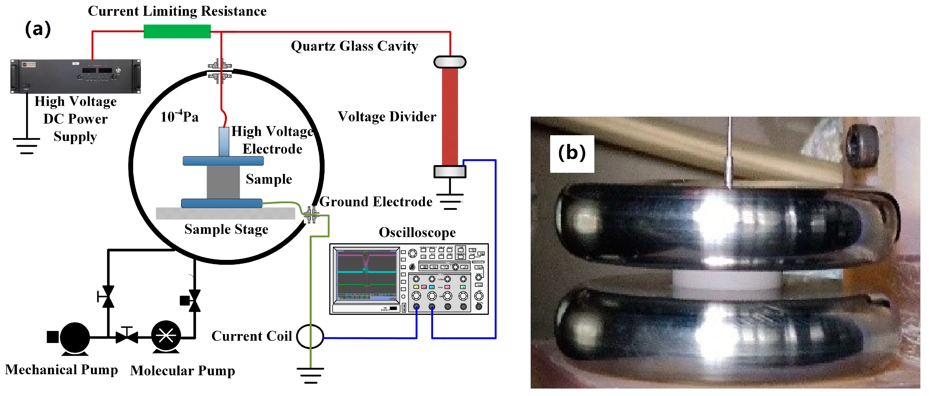
The testing system for withstand voltage of Al2O3 ceramics in vacuum is shown in Figure 3a. The test electrodes are circular plate electrodes made of stainless steel, with the dimensions of Φ66 mm × 10 mm. A photograph of the plate electrodes and sample is shown in Figure 3b. The dimension of the samples for withstand testing is Φ26 mm × 5 mm. The vacuum level in the test chamber is better than 1 × 10⁻⁴ Pa. The test voltage is a negative DC voltage. The testing procedure is as follows: Firstly, the samples undergo thorough conditioning: applying a voltage to the sample until surface flashover occurs, then continuing to increase the voltage to the maximum value. This voltage is then applied repeatedly three times to complete the conditioning of the samples. Subsequently, the voltage is re-applied to the sample with an increasing rate of 500 V/s until a flashover occurs on the ceramic surface. Then, the voltage gradually decreases until the flashover disappears. This process repeats three times. If no flashover occurs on the sample during these repetitions, the voltage at this point is considered the withstand voltage and is denoted as Uho.

3. Results and Discussion

3.1. Thermal Analysis

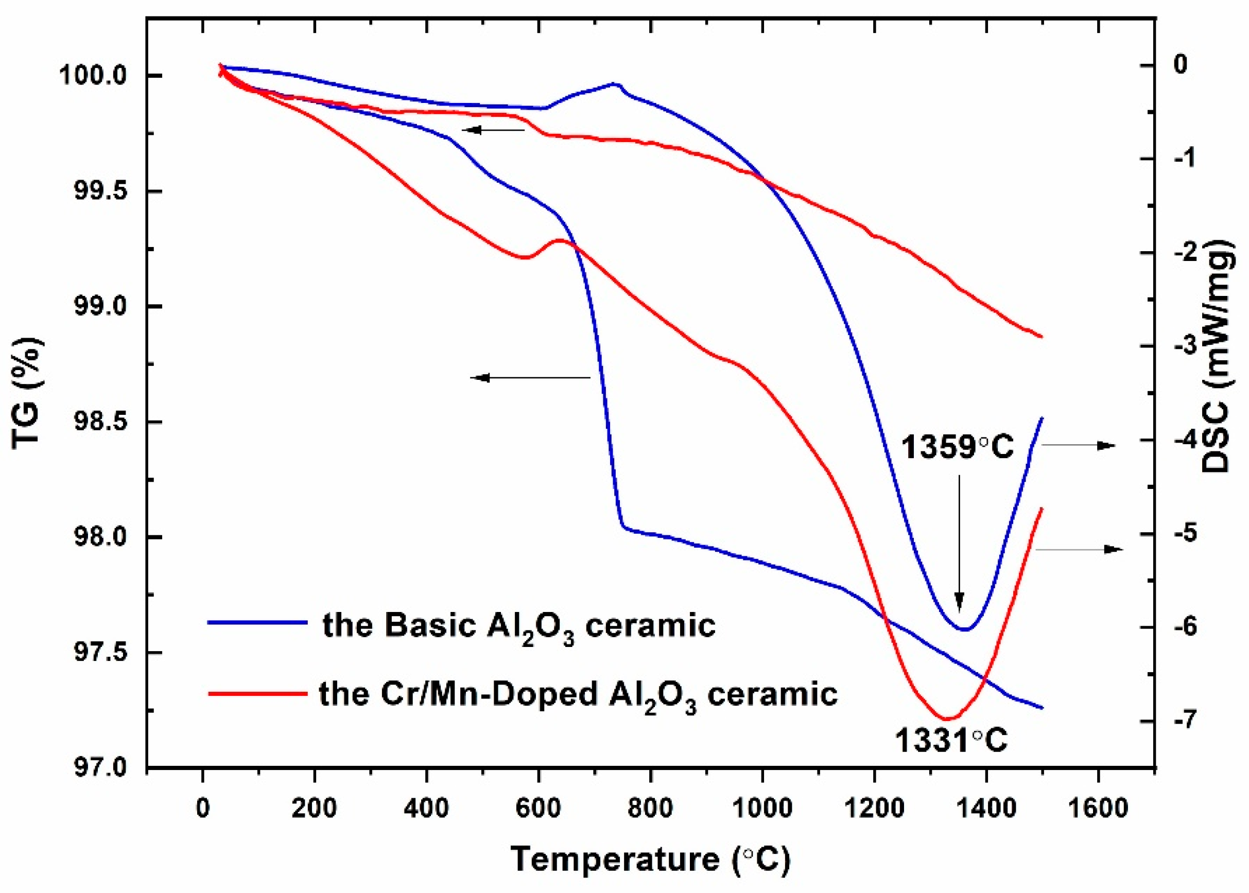
The thermal properties of the basic and the Cr/Mn-doped (Cr2O3: MnO2 = 1:1) Al2O3 ceramics are analyzed by TG-DSC (Thermogravimetric Analysis and Differential Scanning Calorimetry) curves. In Figure 4, the left vertical axis of the TG-DSC curve represents the mass change of the sample, while the right vertical axis corresponds to the DSC curve. The upward and downward peaks, respectively, indicate exothermic and endothermic phenomena occurring in the sample during the heating process. Both basic Al2O3 ceramic and doped Al2O3 ceramic had an endothermic peak before 800 °C, accompanied by a significant mass loss on the TG curve, which was caused by the decomposition of calcium carbonate. Furthermore, there is an obvious endothermic peak between 1300 and 1400 °C on the DSC curve, which corresponds to the initial sintering temperature of Al2O3 ceramic. From Figure 4, we can see that the initial sintering temperature of the Cr/Mn-doped Al2O3 seems to have dropped by 28 °C from 1359 °C to 1331 °C.
This is because Cr2O3 and MnO2 are both hexagonal close-packed structures [29], which is the same as α-Al2O3, and solid solutions of Cr2O3 and MnO2 may form with the Al2O3 lattice [30,31]. Moreover, the differences in electronic structure and electronegativity between Mn4+ and Al3+ may distort and activate the Al2O3 lattice, facilitate the diffusion of particles, and reduce the sintering activation energy, thus promoting sintering and crystalline grain growth. In addition, adding MnO2 to Al2O3 ceramics reduces the low eutectic point of the liquid phase generated during the sintering process, which helps to reduce the sintering temperature of the ceramic.

3.2. Bulk Density and Micromorphology

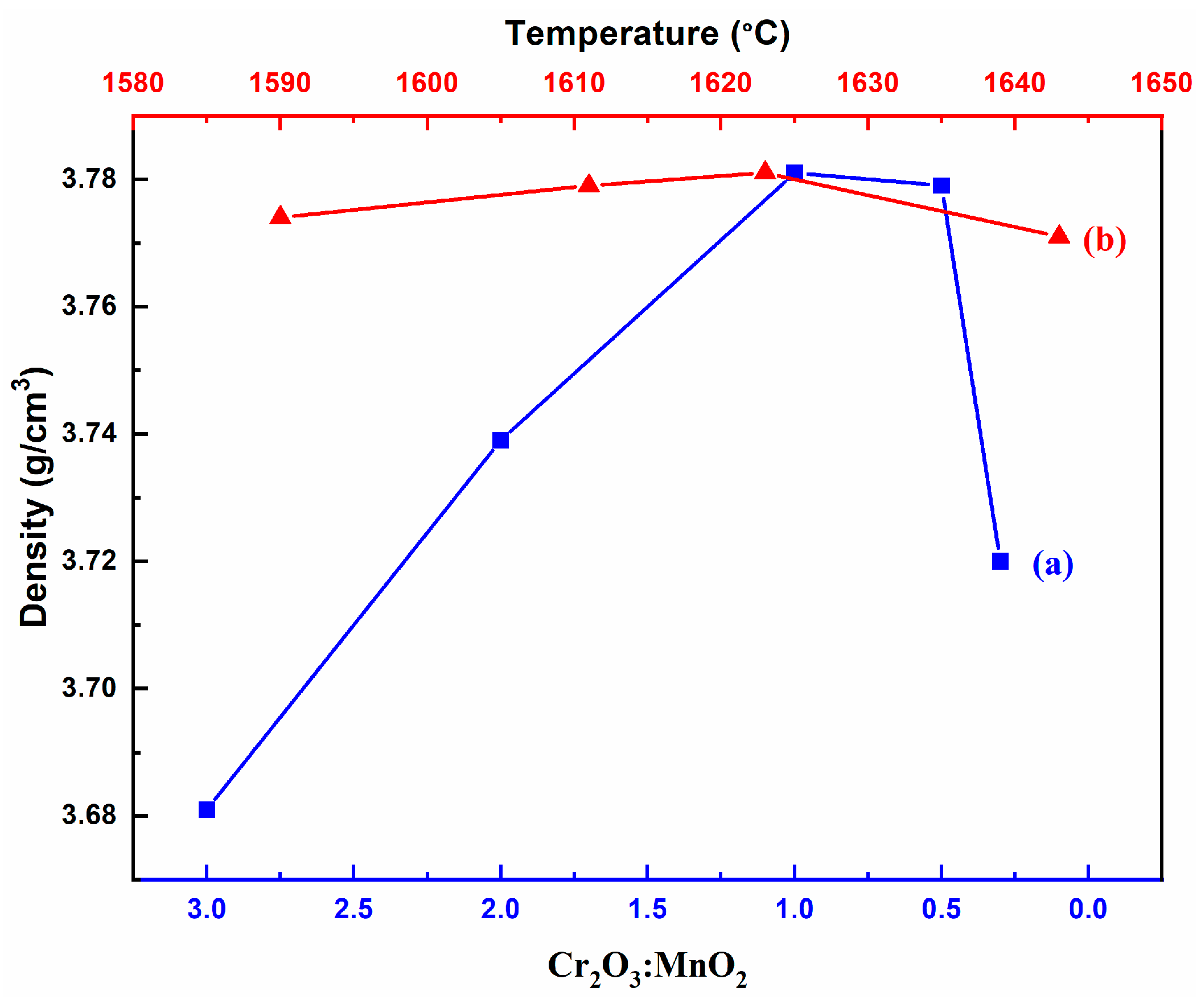
We tested the bulk density and microstructure of Al2O3 ceramics to illustrate the effects of Cr2O3 and MnO2 as additives on the sintering properties of Al2O3 ceramics. From Figure 5, we can see that as the amount of MnO2 addition increases, the volume density of the doped Al2O3 ceramics increases at first and then decreases. On the one hand, due to the relatively high density of MnO2, the addition of MnO2 can contribute to the increase in the bulk density of Al2O3 ceramic. On the other hand, the addition of MnO2 promotes the sintering of Al2O3 ceramic, leading to an increase in the bulk density. Later, with the additional amount of MnO2 increasing continuously, the density of the doped Al2O3 ceramic actually decreases. At the same time, the volume density of the sample (Cr2O3: MnO2 = 1:1) slightly increases at first and then decreases with the increase in sintering temperature. From the thermal analysis of the Al2O3 ceramics, it can be seen that the addition of Cr2O3 and MnO2 promotes ceramic sintering and lowers the sintering temperature of the ceramic. When the sintering temperature is 1623 °C, the volume density of sample CMA12 reaches the maximum value of 3.781 g/cm3. Subsequently, as the sintering temperature continued to increase, the bulk density of the ceramic (Cr2O3: MnO2 = 1:1) decreased because of the occurrence of overburning.
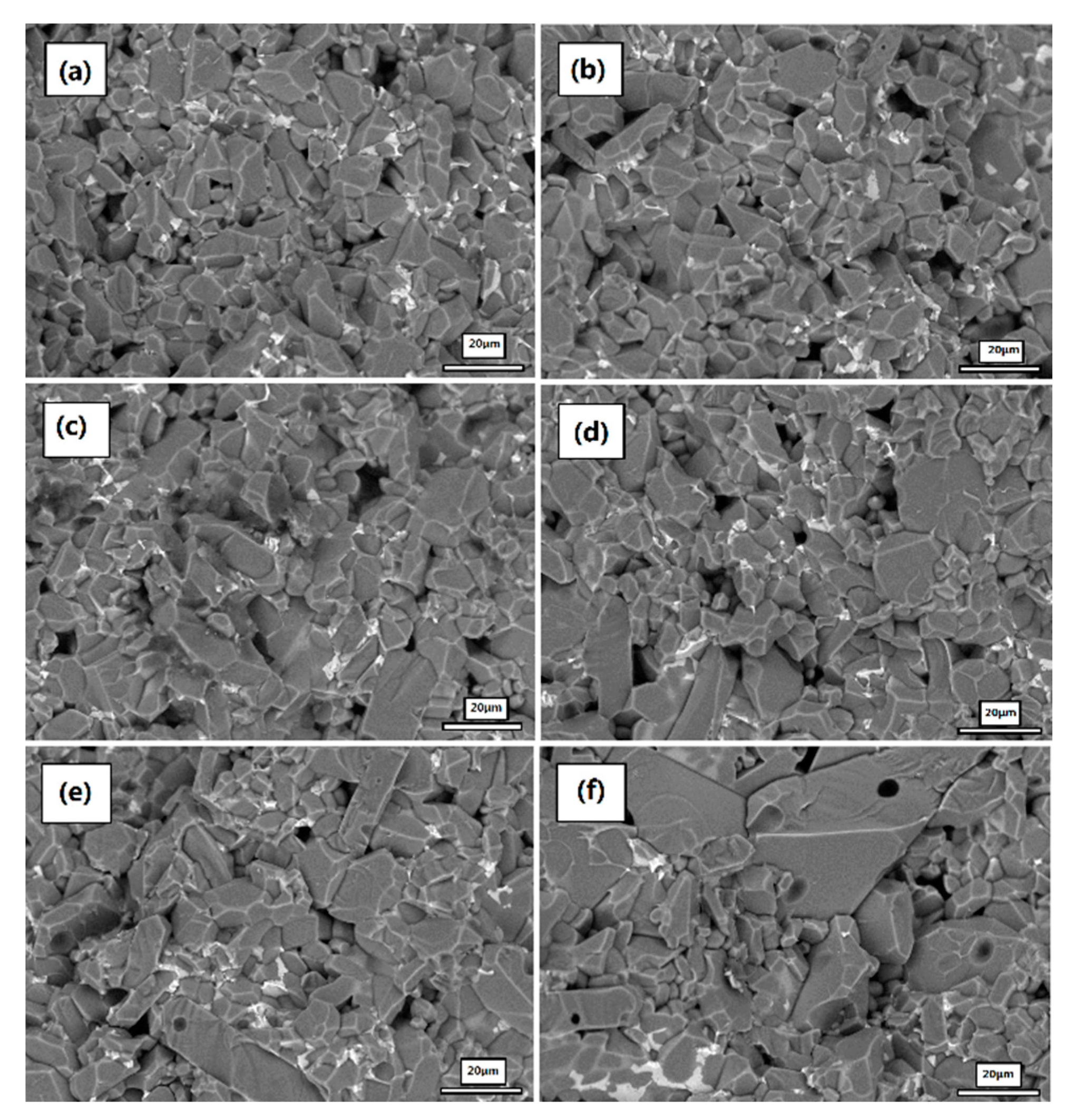
Figure 6 shows the SEM of the Cr/Mn-doped Al2O3 ceramic. When the additional amount of MnO2 increases, the grain size of the ceramic increases. The MnO2 added to Al2O3 ceramics forms a limited solid solution with Al2O3, which promotes the sintering of the ceramics. In addition, as an additive, MnO2 can reduce the eutectic point of the liquid phase during the sintering process of ceramics, which also promotes ceramic sintering. However, when an excessive amount of MnO2 is added, abnormal grain growth occurs in the ceramic. We can observe that in CMA05, especially in the CMA03 sample, there are large-sized grains locally, which will lead to uneven microstructure and reduced density of the material. Figure 6f shows that there are many pores on the grains of the CMA03 sample. This is due to the rapid sintering of the ceramic caused by the addition of a large amount of MnO2, which results in the pores not having enough time to be expelled during the sintering process.

3.3. Phase Composition

To demonstrate the microstructure of the Al2O3 ceramic, the XRD analysis of the samples was performed. From Figure 7, it can be seen that there is only α-Al2O3 crystal phase in the basic ceramic A-0. The major crystal phase in Cr/Mn-doped Al2O3 ceramics is (Al, Cr)2O3. Cr2O3 and Al2O3 crystals had the same lattice type, and Cr3+ and Al3+ had the same ionic valence and similar ionic radius. Cr2O3 dissolved into the Al2O3 lattice, and Cr3+ replaced Al3+, forming a continuous Al2O3-Cr2O3 solid solution [30].
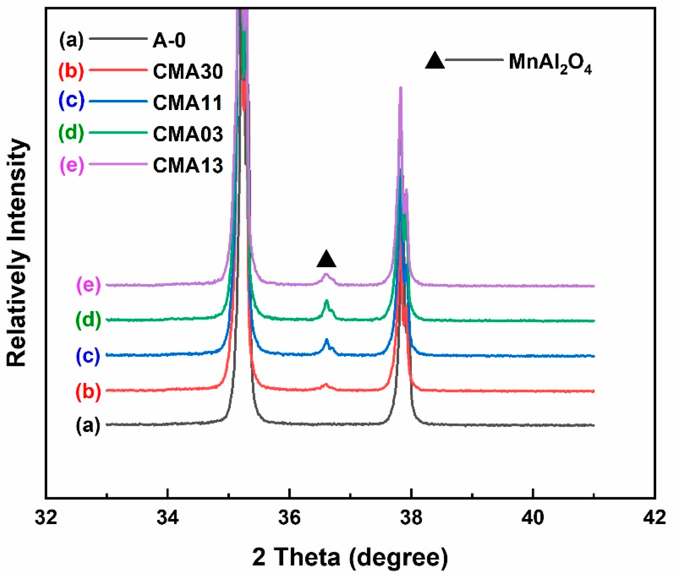
Figure 8 shows that there is also a MnAl2O4 phase in the Cr/Mn-doped Al2O3 ceramic except for the major crystal phase of (Al, Cr)2O3. With a certain amount of MnO2 added to the Al2O3 ceramic, the MnAl2O4 phase will precipitate during the sintering process, which may affect the crystal structure of the ceramics. By normalizing and magnifying the peak of MnAl2O4 at 2 Theta = 37.8 degrees, as shown in Figure 8, it is found that the relative content of MnAl2O4 in the ceramic increases with the increase in the additive amount of MnO2. Meanwhile, the sintering temperature has almost no effect on the type and amount of crystal phases in ceramics.

3.4. Secondary Electron Emission Property

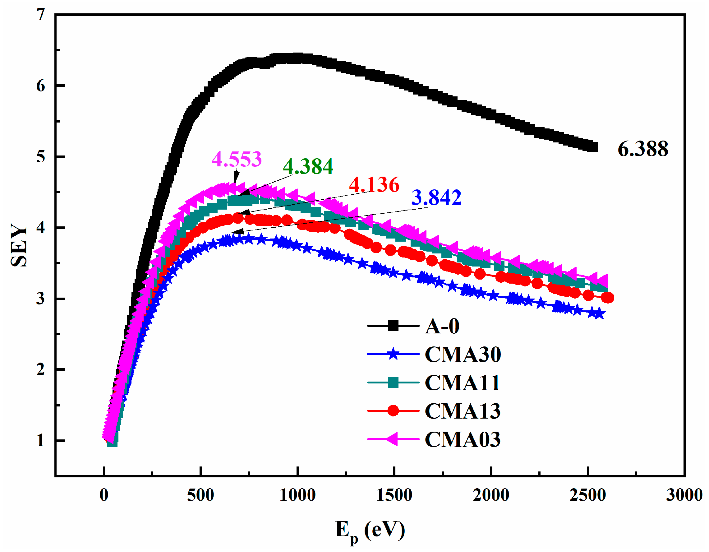
According to the SEEA theory, the SEY of ceramics is the direct cause of the surface flashover in a vacuum, Therefore, to increase the vacuum voltage holdoff capacity of ceramics, it is necessary to reduce their SEY. We tested the SEY of the basic Al2O3 ceramic and the Cr/Mn-doped Al2O3 ceramic, and the secondary electron emission curves are exhibited in Figure 9. We can see that the SEY of Cr/Mn-doped Al2O3 ceramics is significantly lower than 6.388 of the basic Al2O3 ceramic, which is mainly attributed to the addition of Cr2O3 with extremely low SEY. The Cr/Mn-doped Al2O3 ceramics with low SEY are less prone to SEEA phenomena, which is beneficial for improving their withstand voltage in a vacuum. Additionally, as the additive amount of MnO2 and sintering temperature increases, the SEY of the ceramics increases slightly.
The process of the SEEA theory involves the electrons being emitted from the CTJ, accelerated by the electric field, and then colliding with the ceramic surface to excite secondary electrons. These secondary electrons escape from the ceramic surface, under the control of the electric field, and collide with the ceramic again. When the electric field is sufficiently strong, this process can become self-sustaining, leading to a rapid increase in the number of electrons and the occurrence of an electron avalanche. A large number of electrons collide with the gas adsorbed on the ceramic surface, causing the gas to desorb and be ionized by the high-energy electrons, generating a large amount of plasma. Ultimately, surface flashover occurs along the ceramic surface in a vacuum. The main factors influencing the electron avalanche process are the energy of the primary electrons and the ionization energy of the lattice molecules or atoms with which they collide. The ease of collisional ionization is typically quantified by the collisional ionization coefficient α. This coefficient represents the number of ionization events caused by an electron traveling a unit distance under the electric field. The expression of α is as follows:
α = Aexp(−(BVi)/λE)
where Vi is the ionization energy of the collided lattice molecule or atom, λ is the mean free path of the electron, and E is the electric field strength. A and B are constants related to the material. From the above expression, it can be seen that the α is directly affected by the mean free path of electrons. The longer the mean free path of electrons, the longer the time they are subjected to the electric field and the more energy they gain between collisions, making collisional ionization more prone to occur. From the microstructure of the ceramic shown in Figure 6, it can be seen that the grain size increases with higher MnO2 addition and sintering temperature. This leads to a longer time for the electron to be accelerated by the electric field during its escape, enhancing the likelihood of ionization and increasing the SEY consequently.

3.5. Resistivity

As electronic materials, the electrical properties of ceramics have a crucial impact on the performance of devices [32]. The resistivity of ceramic material, especially the surface resistivity, is another key factor influencing its vacuum dielectric strength. Al2O3 ceramics generally have high resistivity, and their high surface resistivity inhibits the leakage of charges accumulated on the ceramic surface. At the same time, it also leads to localized electric field enhancement, making vacuum surface flashover more likely to occur [27,33]. Therefore, in order to improve the withstand voltage of Al2O3 ceramics, it is necessary to reduce their surface resistivity to a certain extent.
As can be seen from Table 3, with the increase in the additional amount of MnO2, the Rs (surface resistance) and Rv (volume resistance) of the Cr/Mn-doped Al2O3 ceramic show a downward trend. The Rs and Rv of Al2O3 ceramics decreased by one order of magnitude when a small amount of MnO2 was added. With a further increase in the amount of MnO2 added, the Rs and Rv of Al2O3 ceramics can decrease by three to four orders of magnitude, reaching 1012 Ω. The influence of MnO2 addition on the resistivity of Al2O3 ceramics can be attributed to the following reasons: MnO2 added to Al2O3 ceramics can dissolve in the Al2O3 crystal lattice, forming a solid solution. However, the ionic valence of Mn4+ and Al3+ are different. When Mn4+ replaces the position of Al3+, it forms an inequivalent substitutional type solid solution. To maintain electrical neutrality, vacancies are generated at the original Al3+ sites. These vacancies form defect centers in the ceramic, serving as charge carriers that facilitate charge transport, thereby reducing the resistivity of the ceramic.

3.6. Withstand Voltage in Vacuum

The voltage holdoff capacity in vacuum of the ceramics was expressed by the withstand voltage. Five ceramic samples are tested for each group, and the average value of Uho is then calculated as the final result of the withstand voltage. The standard deviations of the samples in each group were calculated to characterize the voltage withstand stability of the Al2O3 ceramics. Table 4 shows the withstand voltage in vacuum of the base Al2O3 ceramics and the Cr/Mn-doped Al2O3 ceramics.
From Table 4, we can see that the addition of Cr2O3 and MnO2 to Al2O3 ceramics can significantly increase the value of the withstand voltage and the stability of Al2O3 ceramics. Al2O3 ceramics with an appropriate amount of Cr2O3 and MnO2 and sintered at suitable temperatures exhibit high withstand voltage and stability. The Uho of CMA13 reached 31 kV, which was 24% higher than that of the basic Al2O3 ceramic. In addition, its standard deviation reached the minimum value, indicating a high voltage withstand stability. The Uho of the Al2O3 ceramics was improved by the addition of Cr2O3 and MnO2 for the following reasons: Firstly, the SEY of the Cr/Mn-doped Al2O3 ceramics is significantly lower than that of the basic Al2O3 ceramics, making it less likely for SEEA to occur when a voltage is applied. As a result, the withstand voltage increases. Secondly, the resistivity of the CMA11 sample is reduced by one order of magnitude compared to the basic Al2O3 ceramic, facilitating charge dissipation from the ceramic surface. The decrease in resistivity can accelerate the leakage of charges accumulated on the ceramic surface, reduce the probability of surface flashover, and improve the surface withstand voltage. Finally, by adding an appropriate amount of Cr2O3 and MnO2 and sintering at a suitable temperature, Al2O3 ceramics with uniform and compact microstructure can be prepared, which can enhance the voltage withstand stability of the ceramic.
The Uho of the CMA14 sample reached the maximum value of 32 kV, but the stability decreased, which may lead to poor reliability of vacuum devices in use. This is because the sintering temperature was too high, resulting in the oversintering of the ceramic. The microstructure and density of the ceramic became worse. With the crystalline grains in the samples growing abnormally, many closed pores appeared in the grains and at the grain boundary, leading to the uneven distribution of grain size [34,35]. These defects in the material become traps for capturing charges and form equilibrium states in the process of dielectric polarization [36]. This may be a contributing factor to the poor voltage withstand stability of the doped Al2O3 ceramic sintered at 1643 °C.
The withstand voltage and stability of CMA05 and CMA03 samples are significantly reduced. Although the Rs of CMA05 and CMA03 samples decreased by two to three orders of magnitude, which is more conducive to the release of surface charges on the ceramic, the microstructure and density of CMA05 and CMA03 samples deteriorated, leading to a decline in their surface withstand voltage performance. In this study, the CMA03 and CMA05 samples did not exhibit the beneficial effect of reduced resistivity on the withstand voltage performance of the ceramics in a vacuum.

4. Conclusions

In this study, the influence of the addition ratio of Cr2O3 on MnO2 and the sintering temperature was investigated, and the SEY and resistivity of Al2O3 ceramic were reduced by adding Cr2O3 and MnO2. Cr/Mn-doped Al2O3 ceramics with excellent withstand voltage properties were prepared. The main conclusions are as follows:
(1)
Cr2O3 and MnO2 have an influence on the microstructure and the sintering performance of Al2O3 ceramics. Al2O3 ceramics with an appropriate amount of Cr2O3 and MnO2, sintered at 1623 °C, exhibit uniform and dense microstructure and high voltage withstand stability.
(2)
The addition of Cr2O3 and MnO2 significantly reduced the SEY and Rs of Al2O3 ceramics. Compared to basic Al2O3 ceramics, the SEY of Cr/Mn-doped Al2O3 ceramics decreased by about 50%, while the Rs of Cr/Mn-doped Al2O3 ceramics decreased by up to three orders of magnitude.
(3)
The withstand voltage properties of the prepared Cr/Mn-doped Al2O3 ceramics are significantly improved. The Uho of the CMA13 sample reached 31 kV, which was 24% higher than that of the basic Al2O3 ceramics. In addition, the voltage withstand stability of the CMA13 sample was relatively high.

Author Contributions

Conceptualization, D.F.; Methodology, D.F., X.H. and X.W.; Validation, D.F. and X.W.; Formal Analysis, D.F. and H.W.; Investigation, D.F.; Data Curation, D.F., X.H., Z.Y. and J.F.; Writing—Original Draft Preparation, D.F.; Writing—Review and Editing, X.W.; Supervision, Z.Y. and J.F.; Project Administration, Z.Y. Funding Acquisition, H.W. All authors have read and agreed to the published version of the manuscript.

Funding

This work was supported by a grant from the National Key Research and Development Program of China, “Basic scientific research conditions and national major scientific instruments and equipment development” (No. 2022YFF0707400).

Data Availability Statement

The original contributions presented in this study are included in the article. Further inquiries can be directed to the corresponding author.

Acknowledgments

This work was completed at Beijing Vacuum Electronic Research Institute, Beijing University. Thank you to all team members for their efforts in this research.

Conflicts of Interest

The authors declare no conflicts of interest.

References

  1. Olsommer, Y.; Ihmig, F.R. Experimental Characterization of Ferroelectric Capacitor Circuits for the Realization of Simply Designed Electroceuticals. Electron. Mater. 2021, 2, 299–311. [Google Scholar] [CrossRef]
  2. Vanjaria, J.; Hariharan, V.; Arjunan, A.C.; Wu, Y.; Tompa, G.S.; Yu, H. One-Step Cost-Effective Growth of High-Quality Epitaxial Ge Films on Si (100) Using a Simplified PECVD Reactor. Electron. Mater. 2021, 2, 482–494. [Google Scholar] [CrossRef]
  3. Suchaneck, G.; Artiukh, E.; Kalanda, N.; Yarmolich, M.; Gerlach, G. Nanogranular Strontium Ferromolybdate/Strontium Molybdate Ceramics—A Magnetic Material Possessing a Natural Core-Shell Structure. Electron. Mater. 2024, 5, 1–16. [Google Scholar] [CrossRef]
  4. Goswami, A.P.; Roy, S.; Das, G.C. Effect of powder, chemistry and morphology on the dielectric properties of liquid-phase-sintered alumina. Ceram. Int. 2002, 28, 439–445. [Google Scholar] [CrossRef]
  5. Naseer, D.; Ha, J.H.; Lee, J.; Song, I.H. Preparation of Al2O3 Multichannel Cylindrical-Tube-Type Microfiltration Membrane with Surface Modification. Appl. Sci. 2022, 12, 7993. [Google Scholar] [CrossRef]
  6. Ahmad, R.; Kim, J.K.; Kim, J.H.; Kim, J. Nanostructured Ceramic Photocatalytic Membrane Modified with a Polymer Template for Textile Wastewater Treatment. Appl. Sci. 2017, 7, 1824. [Google Scholar] [CrossRef]
  7. Aleksandr, K.; Ilya, B.; Aleksey, Z. Electron-Beam Processing of Aluminum-Containing Ceramics in the Forevacuum Pressure Range. Ceramics 2023, 6, 2098–2116. [Google Scholar] [CrossRef]
  8. Sun, G.-Y.; Guo, B.-H.; Mu, H.-B.; Song, B.-P.; Zhou, R.-D.; Zhang, S.; Zhang, G.-J. Flashover strength improvement and multipactor suppression in vacuum using surface charge preconditioning on insulator. J. Appl. Phys. 2018, 124, 134102. [Google Scholar] [CrossRef]
  9. Pillai, A.S.; Hackam, R. Surface flashover of solid insulators in atmospheric air and in vacuum. J. Appl. Phys. 1985, 58, 146–153. [Google Scholar] [CrossRef]
  10. Miller, C.H. Flashover of insulators in vacuum: The last twenty years. IEEE Trans. Dielectr. Electr. Insul. 2016, 22, 3641–3657. [Google Scholar] [CrossRef]
  11. Yan, P.; Shao, T.; Wang, J.; Gao, W.; Yuan, W.; Pan, R.; Zhang, S.; Sun, G. Experimental investigation of surface flashover in vacuum using nanosecond pulses. IEEE Trans. Dielectr. Electr. Insul. 2007, 14, 634–642. [Google Scholar] [CrossRef]
  12. Liebault, J.; Vallayer, J.; Goeuriot, D.; Treheux, D.; Thevenot, F. How the trapping of charges can explain the dielectric breakdown performance of alumina ceramics. J. Eur. Ceram. Soc. 2001, 21, 389–397. [Google Scholar] [CrossRef]
  13. Hawley, R. Solid insulators in vacuum: A Review. Vacuum 1968, V18, 383–390. [Google Scholar] [CrossRef]
  14. Seif, M.N.; Balk, T.J.; Beck, M.J. Desorption from Hot Scandate Cathodes: Effects on Vacuum Device Interior Surfaces after Long-Term Operation. Materials 2020, 13, 5149. [Google Scholar] [CrossRef]
  15. Li, S. Improvement of surface flashover in vacuum. High Volt. 2020, 5, 122–133. [Google Scholar] [CrossRef]
  16. Vlieks, A.E.; Allen, M.A.; Callin, R.S.; Fowkes, W.R.; Hoyt, E.W.; Lebacqz, J.V.; Lee, T.G. Breakdown phenomena in high power klystrons. IEEE Trans. Electr. Insul. 1989, 24, 1023–1028. [Google Scholar] [CrossRef]
  17. Tafazoli, M. A study of on-orbit spacecraft failures. Acta Astronaut. 2009, 64, 195–205. [Google Scholar] [CrossRef]
  18. Tyunkov, A.V.; Klimov, A.S.; Savkin, K.P.; Yushkov, Y.G.; Zolotukhin, D.B. Electron-Beam Deposition of Metal and Ceramic-Based Composite Coatings in the Fore-Vacuum Pressure Range. Ceramics 2022, 5, 789–797. [Google Scholar] [CrossRef]
  19. Jang, S.O.; Cho, C.; Kim, J.H.; Kang, I.J.; Chang, H.; Park, H.; Lee, K.; Kim, D.G.; Seok, H.W. Microwave Plasma Assisted Aerosol Deposition (µ-PAD) for Ceramic Coating Applications. Ceramics 2022, 5, 1174–1184. [Google Scholar] [CrossRef]
  20. Anderson, R.A.; Tucker, W.K. Vacuum surface flashover from bipolar stress. J. Appl. Phys. 1985, 58, 3346–3349. [Google Scholar] [CrossRef]
  21. Anderson, R.A. Mechanism of pulsed surface flashover involving electron-stimulated desorption. J. Appl. Phys. 1980, 51, 1414–1421. [Google Scholar] [CrossRef]
  22. Cross, J. High speed photography of surface flashover in vacuum. IEEE Trans. Electr. Insul. 1978, EI-13, 145–148. [Google Scholar] [CrossRef]
  23. Sudarshan, T.S.; Cross, J.D. The Effect of Chromium Oxide Coatings on Surface Flashover of Alumina Spacers in Vacuum. IEEE Trans. Electr. Insul. 1976, EI-11, 32–35. [Google Scholar] [CrossRef]
  24. Zheng, J.G.; Jiang, L.X.; Cai, Y.P.; Luo, S.W.; Zhou, X.M. Secondary Electron Emission Characteristic of Insulated Al2O3 Ceramics with Cr2O3 Coating. J. Inorg. Mater. 2001, 16, 497–502. [Google Scholar]
  25. Hosono, T.; Kato, K.; Morita, A.; Okubo, H. Charging Control on Alumina Surface in Vacuum by Surface Roughness and Electric Field Distribution. In Proceedings of the 2006 International Symposium on Discharges and Electrical Insulation in Vacuum, Matsue, Japan, 25–29 September 2006. [Google Scholar]
  26. Zhang, H.; Xu, Y.; Qiao, G.; Ma, D.; Jin, H. Effects of Cr2O3 Addition on Microstructure and Vacuum Flashover Performance of Glass-Ceramics. IEEE Trans. Dielectr. Electr. Insul. 2014, 21, 1882–1886. [Google Scholar] [CrossRef]
  27. Wang, F.; He, L.; Khan, M.Z.; Zhang, T.; Zhao, Q.; He, Y.; Huang, Z.; Zhao, H.; Li, J. Accelerated Charge Dissipation by Gas-Phase Fluorination on Nomex Paper. Appl. Sci. 2019, 9, 3879. [Google Scholar] [CrossRef]
  28. Cai, Y.; Wang, D.; Qi, K.; He, Y. Measurement of total electron emission yield of insulators based on self-terminating charge neutralization. Rev. Sci. Instrum. 2022, 93, 055103-1–055103-7. [Google Scholar] [CrossRef]
  29. Hauet, T.; Piraux, L.; Srivastava, S.K.; Antohe, V.A.; Lacour, D.; Hehn, M.; Montaigne, F.; Schwenk, J.; Marioni, M.A.; Hug, H.J.; et al. Reversal mechanism, switching field distribution, and dipolar frustrations in Co/Pt bit pattern media based on auto-assembled anodic alumina hexagonal nanobump arrays. Phys. Rev. B 2014, 89, 174421. [Google Scholar] [CrossRef]
  30. Shinozaki, K.; Ishikura, Y.; Uematsu, K.; Mizutani, N.; Kato, M. The sintering behavior and mechanical properties of the MgO doped Al2O3-Cr2O3 solid solution. Nippon. Kagaku Kaishi 1981, 7, 1093–1098. [Google Scholar] [CrossRef]
  31. Klimov, A.; Bakeev, I.; Dolgova, A.; Oks, E.; Tran, V.T.; Zenin, A. Electron-Beam Sintering of Al2O3-Cr-Based Composites Using a Forevacuum Electron Source. Ceramics 2022, 5, 748–760. [Google Scholar] [CrossRef]
  32. Molak, A.; Szeremeta, A.Z.; Koperski, J. Vis and NIR Diffuse Reflectance Study in Disordered Bismuth Manganate—Lead Titanate Ceramics. Electron. Mater. 2022, 3, 101–114. [Google Scholar] [CrossRef]
  33. Grigoriev, S.N.; Volosova, M.A.; Peretyagin, P.Y.; Seleznev, A.E.; Okunkova, A.A.; Smirnov, A. The Effect of TiC Additive on Mechanical and Electrical Properties of Al2O3 Ceramic. Appl. Sci. 2018, 8, 2385. [Google Scholar] [CrossRef]
  34. Huang, Y.; Min, D.; Li, S.; Li, Z.; Xie, D.; Wang, X.; Lin, S. Surface flashover performance of epoxy resin microcomposites improved by electron beam irradiation. Appl. Surf. Sci. A J. Devoted Prop. Interfaces Relat. Synth. Behav. Mater. 2017, 406, 39–45. [Google Scholar] [CrossRef]
  35. Du, B.X.; Li, J.; Du, W. Surface charge accumulation and decay on directfluorinated polyimide/Al2O3 nanocomposites. IEEE Trans. Dielectr. Electr. Insul. 2013, 20, 1764–1771. [Google Scholar] [CrossRef]
  36. Sudarshan, T.S.; Li, C.R. Dielectric surface flashover in vacuum. Experimental design issues. IEEE Trans. Dielectr. Electr. Insul. 1997, 4, 657–662. [Google Scholar] [CrossRef]
Figure 1. Flow chart of the preparation of the Al2O3 ceramics.
Electronicmat 06 00004 g001
Figure 2. Diagrammatic sketch of the test system of secondary electron emission property.
Electronicmat 06 00004 g002
Figure 3. (a) Diagrammatic sketch of the testing system for withstand voltage in vacuum; (b) photo of the plate electrodes and testing structure.
Electronicmat 06 00004 g003
Figure 4. TG-DSC (Thermogravimetric Analysis and Differential Scanning Calorimetry) curves of the basic and Cr/Mn-doped Al2O3 ceramics.
Electronicmat 06 00004 g004
Figure 5. The variation of bulk density of Cr/Mn-doped Al2O3 ceramics with the addition ratio of Cr2O3 to MnO2 and sintering temperatures: (a) Sintering temperature of 1623 °C; (b) Cr2O3:MnO2 = 1:1.
Electronicmat 06 00004 g005
Figure 6. SEM of Cr/Mn-doped Al2O3 ceramics: (a) CMA30; (b) CMA20; (c) CMA13; (d) CMA14; (e) CMA05; and (f) CMA03.
Electronicmat 06 00004 g006
Figure 7. The XRD patterns of the Al2O3 ceramic.
Electronicmat 06 00004 g007
Figure 8. Normalized and magnified local XRD patterns of Al2O3 ceramics.
Electronicmat 06 00004 g008
Figure 9. Secondary electron emission curves of the Al2O3 ceramics.
Electronicmat 06 00004 g009
Table 1. Sintering program of the Al2O3 ceramics.
Temperature, °C25–520520–520520–11001100–13001300–**–*
Time, h523234
Table 2. Numbers for samples with varying addition ratios of Cr2O3 to MnO2 and sintering temperatures.
SampleCr2O3: MnO2Sintering Temperature, °C
A-0-1645
CMA303:11623
CMA202:11623
CMA111:11590
CMA121:11611
CMA131:11623
CMA141:11643
CMA051:21623
CMA031:31623
Table 3. Resistivity of the Al2O3 ceramics.
SampleRs (Surface Resistance), ΩRv (Volume Resistance), Ω·cm
A-07.41 × 10152.35 × 1016
CMA304.78 × 10141.23 × 1016
CMA201.56 × 10145.23 × 1015
CMA117.55 × 10146.46 × 1015
CMA127.21 × 10143.81 × 1015
CMA135.32 × 10144.81 × 1015
CMA145.62 × 10143.48 × 1015
CMA058.94 × 10138.37 × 1014
CMA033.44 × 10121.64 × 1012
Table 4. Value of the withstand voltage and the stability of the Al2O3.
SampleUho, kVUho, kVStandard Deviation, kV
A-01823263126254.76
CMA302327283230283.39
CMA202230282730293.28
CMA112325232925252.45
CMA122825303128282.30
CMA133032282935312.77
CMA143527263637325.26
CMA052428342318255.98
CMA031933232430265.63
Disclaimer/Publisher’s Note: The statements, opinions and data contained in all publications are solely those of the individual author(s) and contributor(s) and not of MDPI and/or the editor(s). MDPI and/or the editor(s) disclaim responsibility for any injury to people or property resulting from any ideas, methods, instructions or products referred to in the content.