
Horn Antenna on Chip Operating at 180 GHz Using the SiGe CMOS Process


Abstract
:1. Introduction
2. Antenna Design
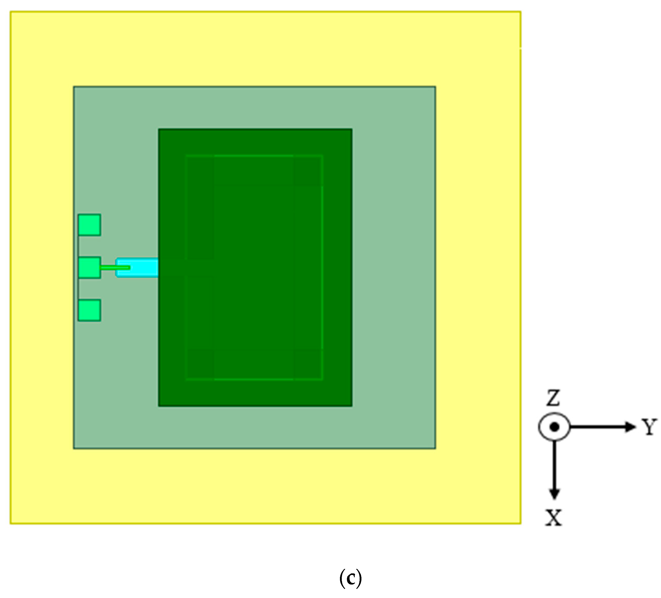
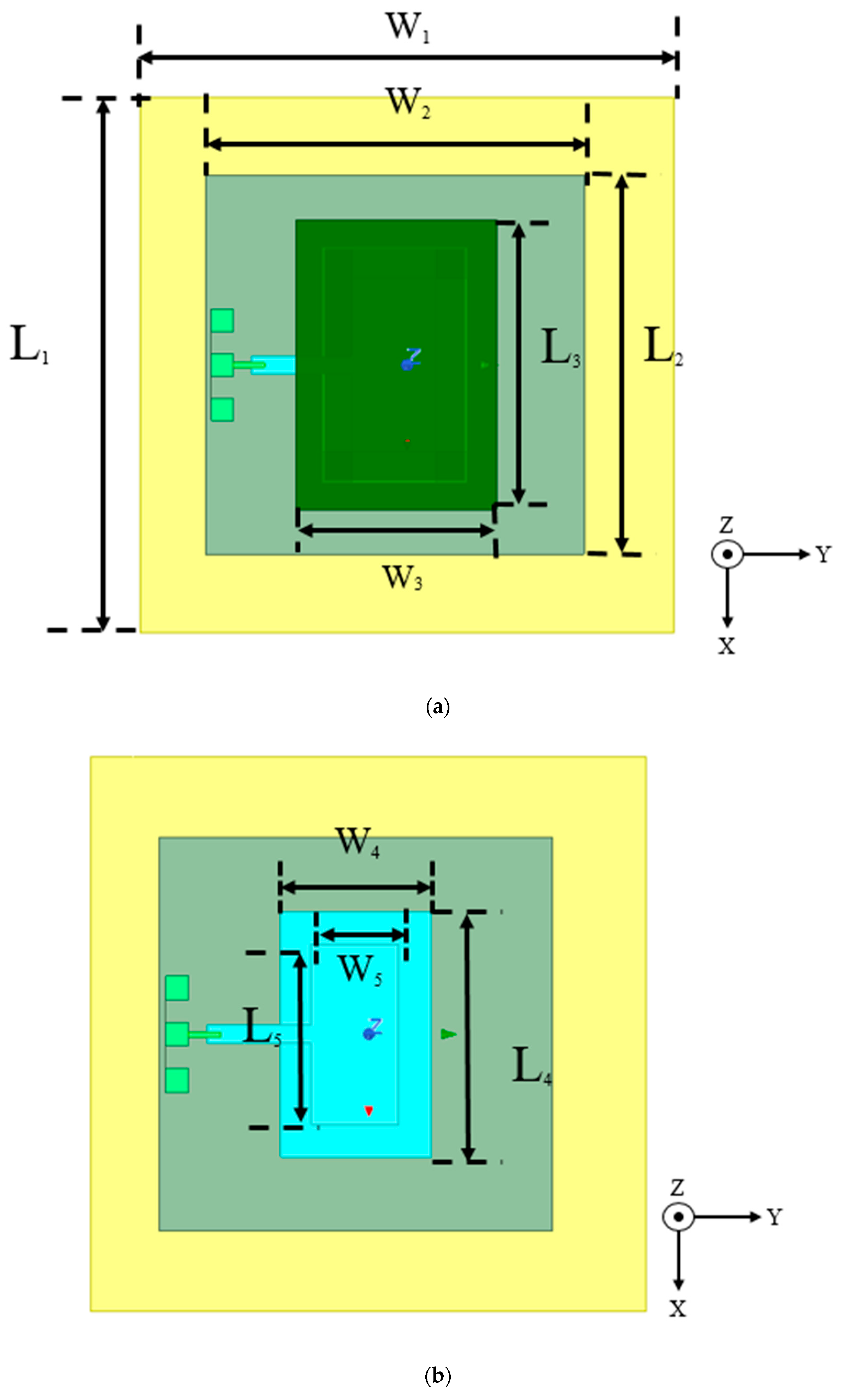
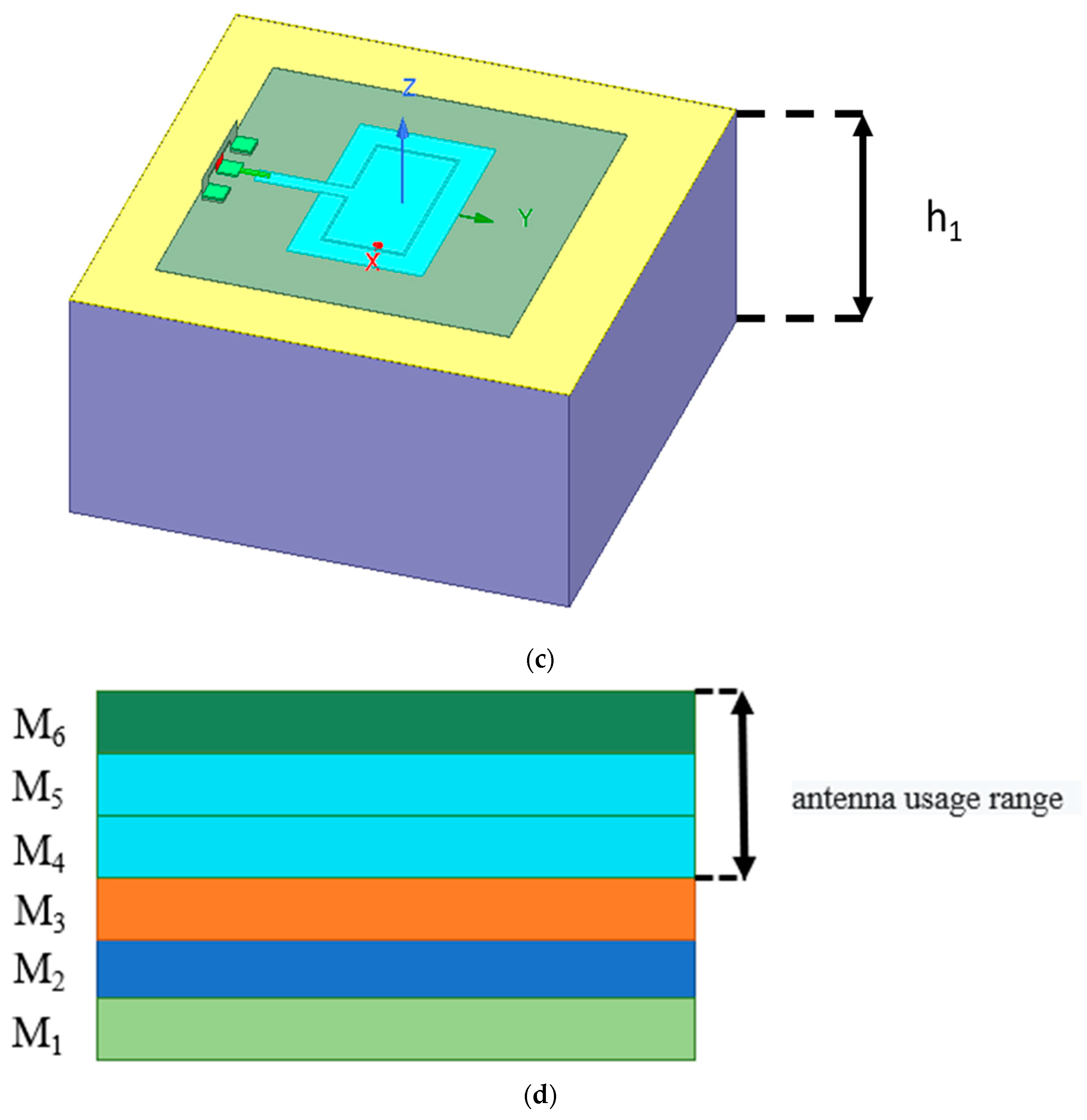
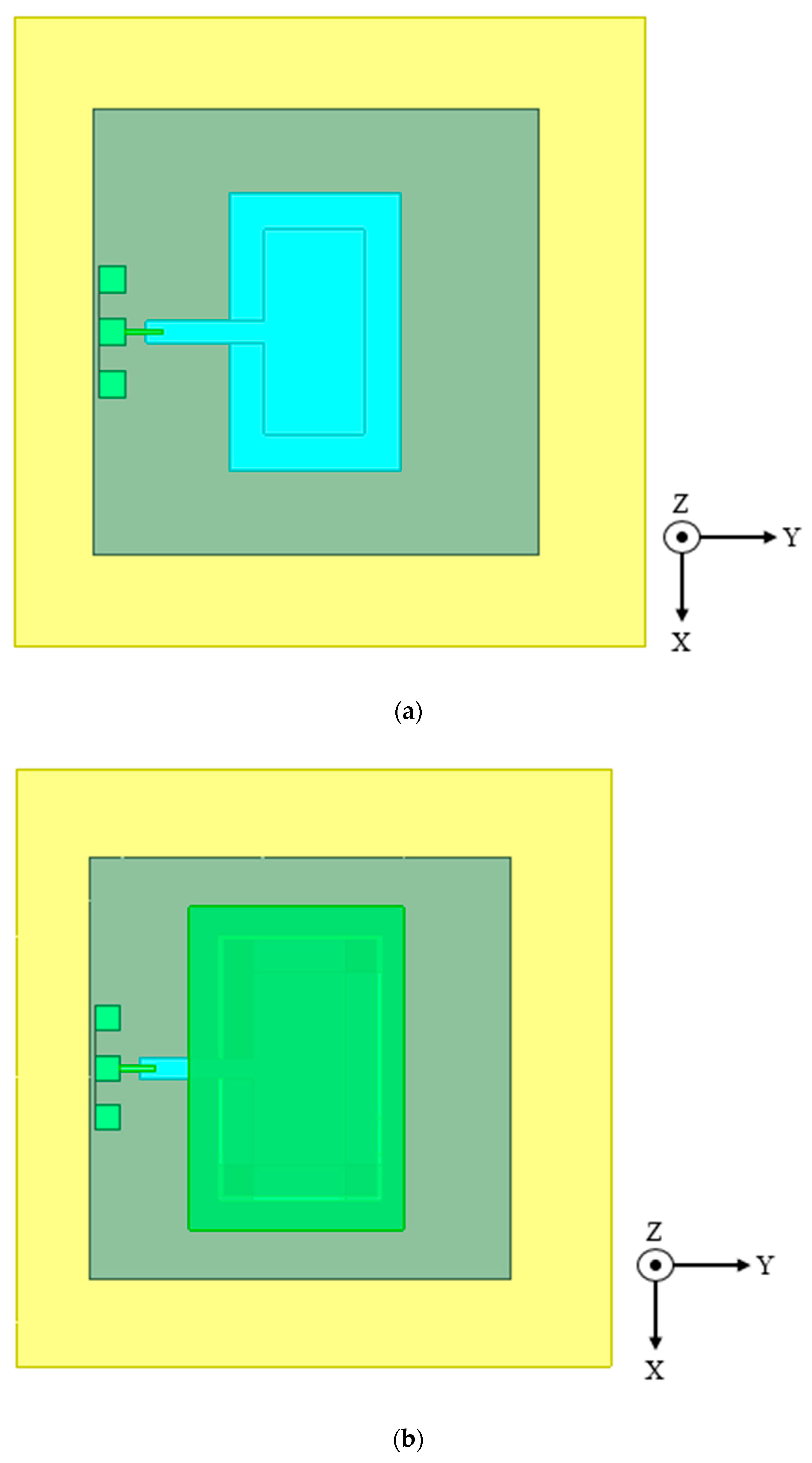
2.1. Configuration
2.2. Evolution of the Antenna
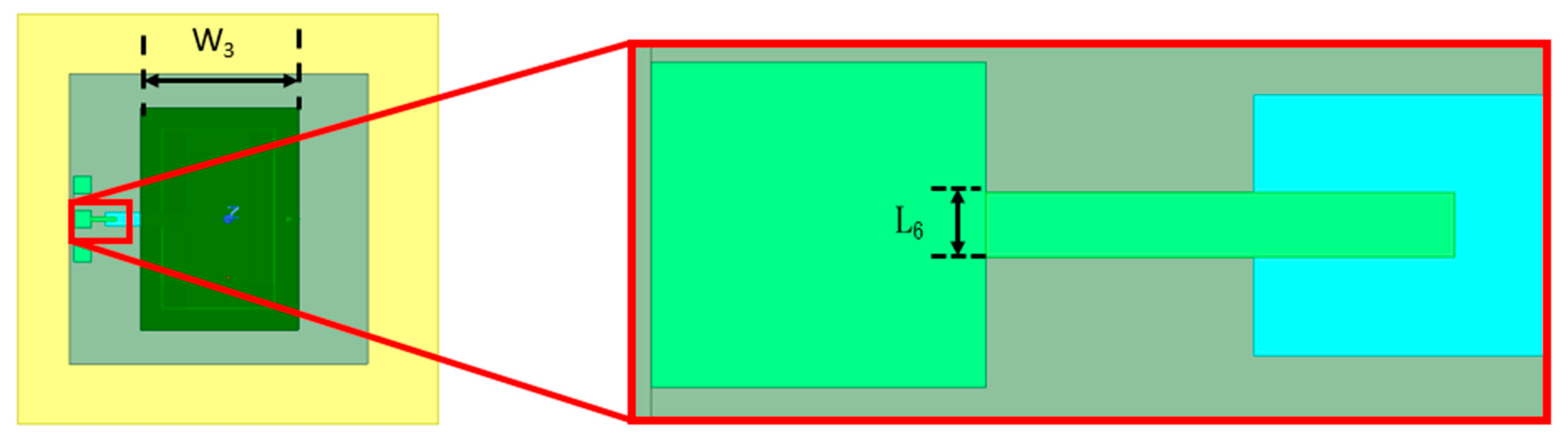
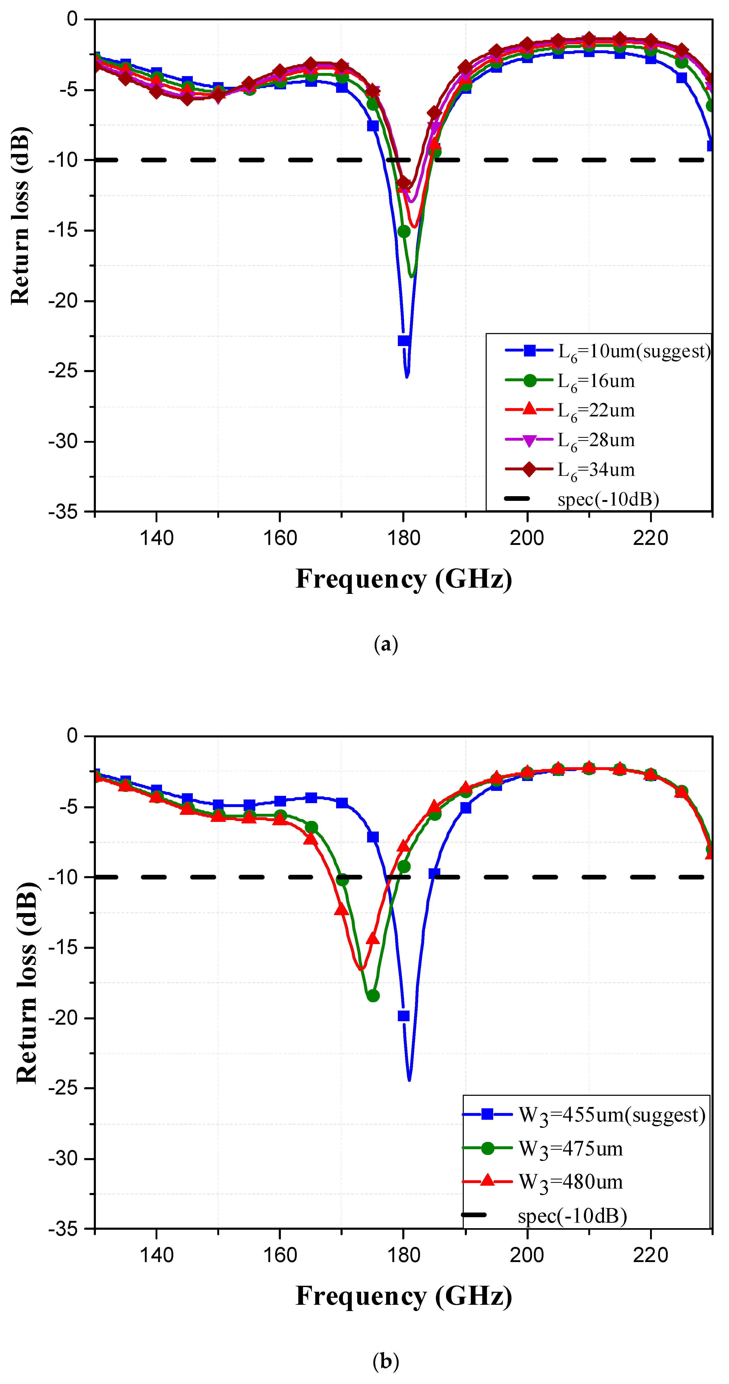
2.3. Parameter Analysis
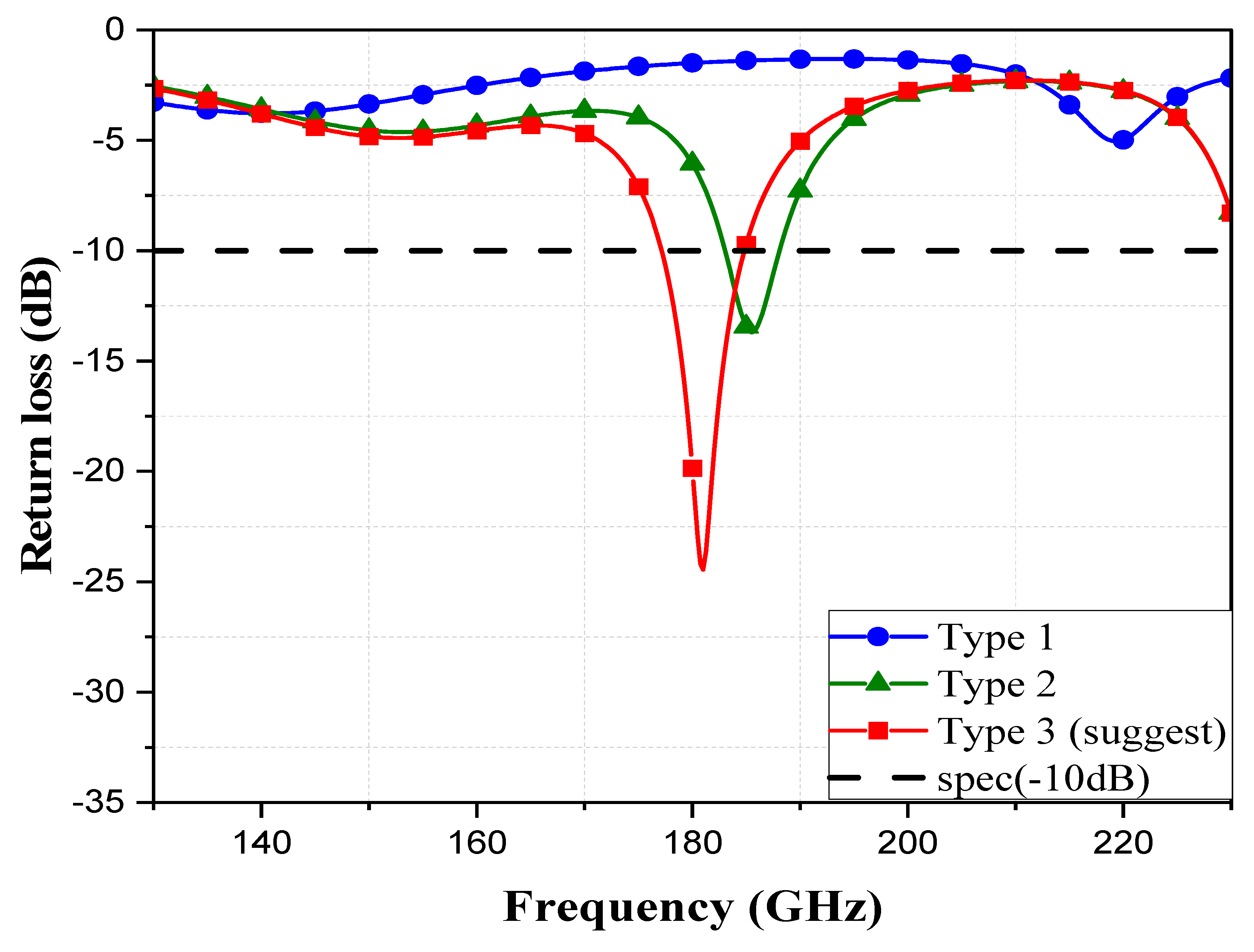
3. Simulation and Measurement
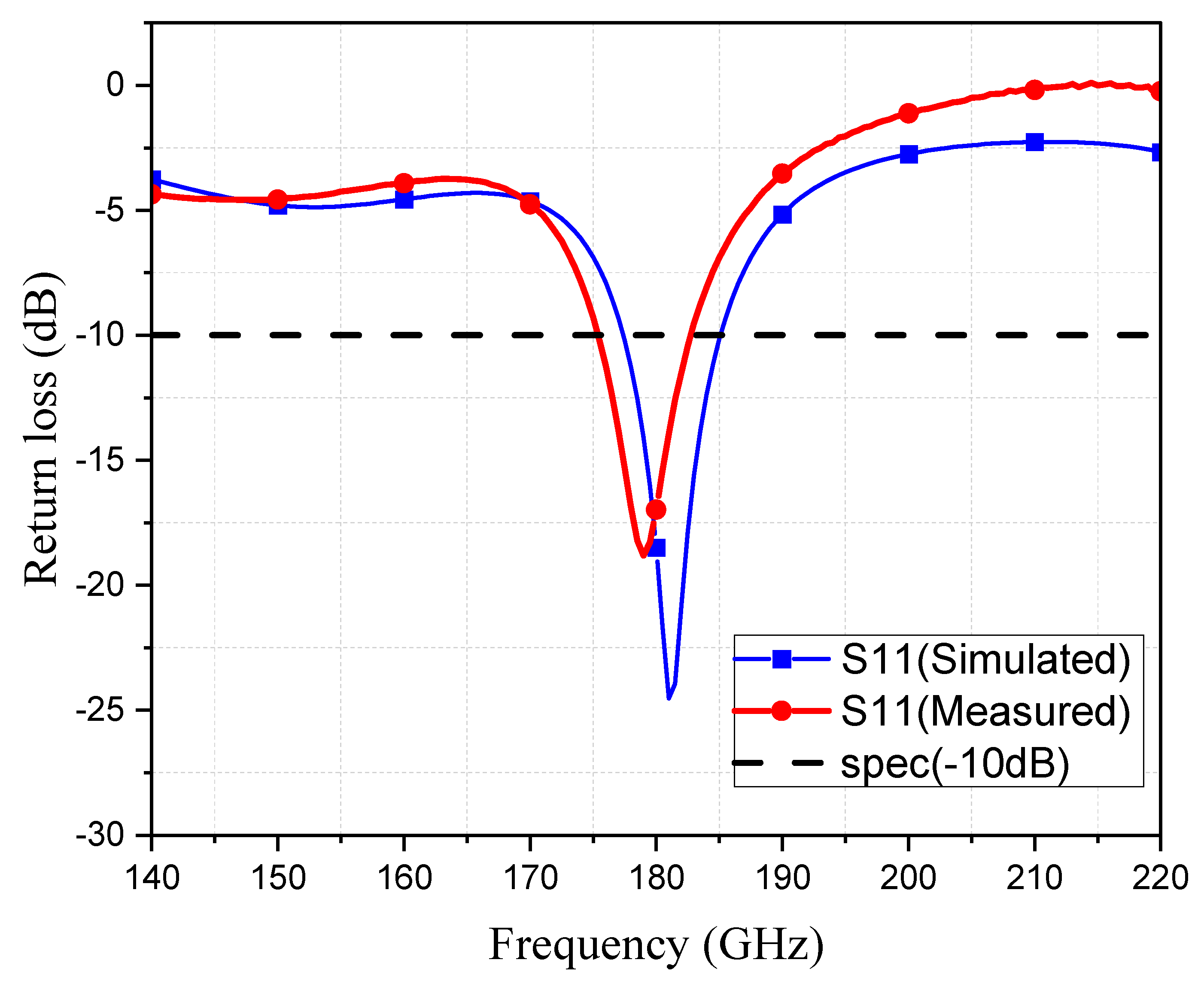
3.1. Return Loss
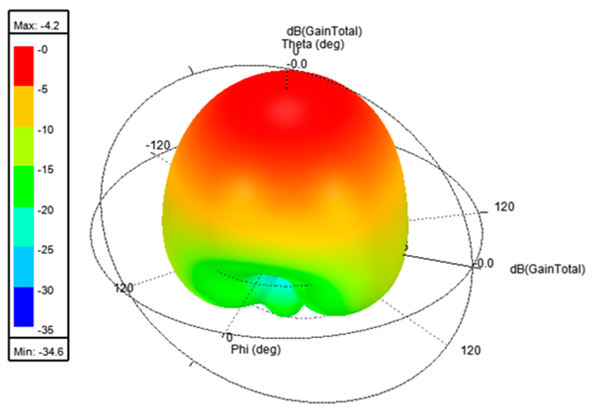
3.2. 3D Radiation Pattern
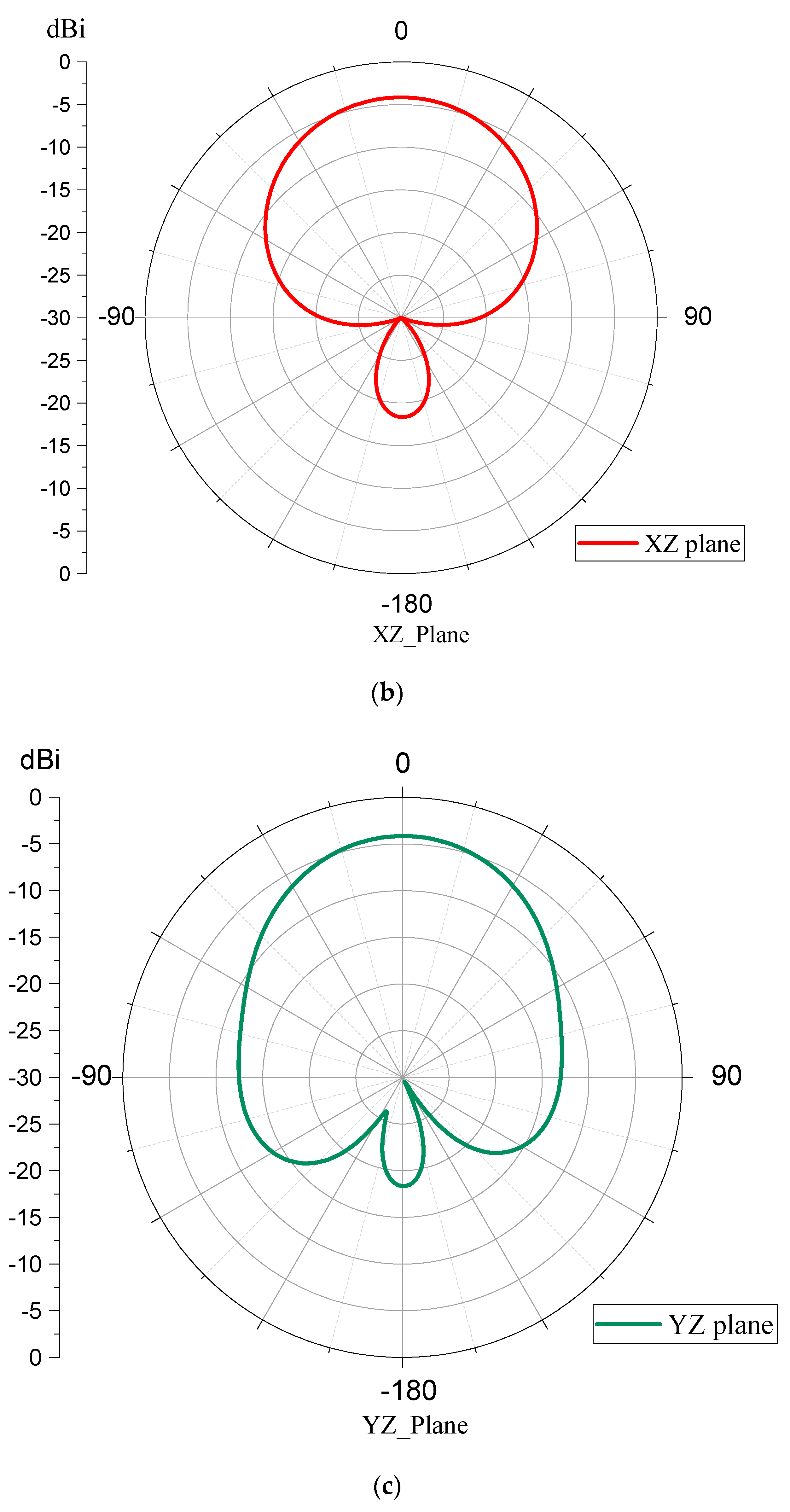
3.3. 2D Radiation Pattern Diagram
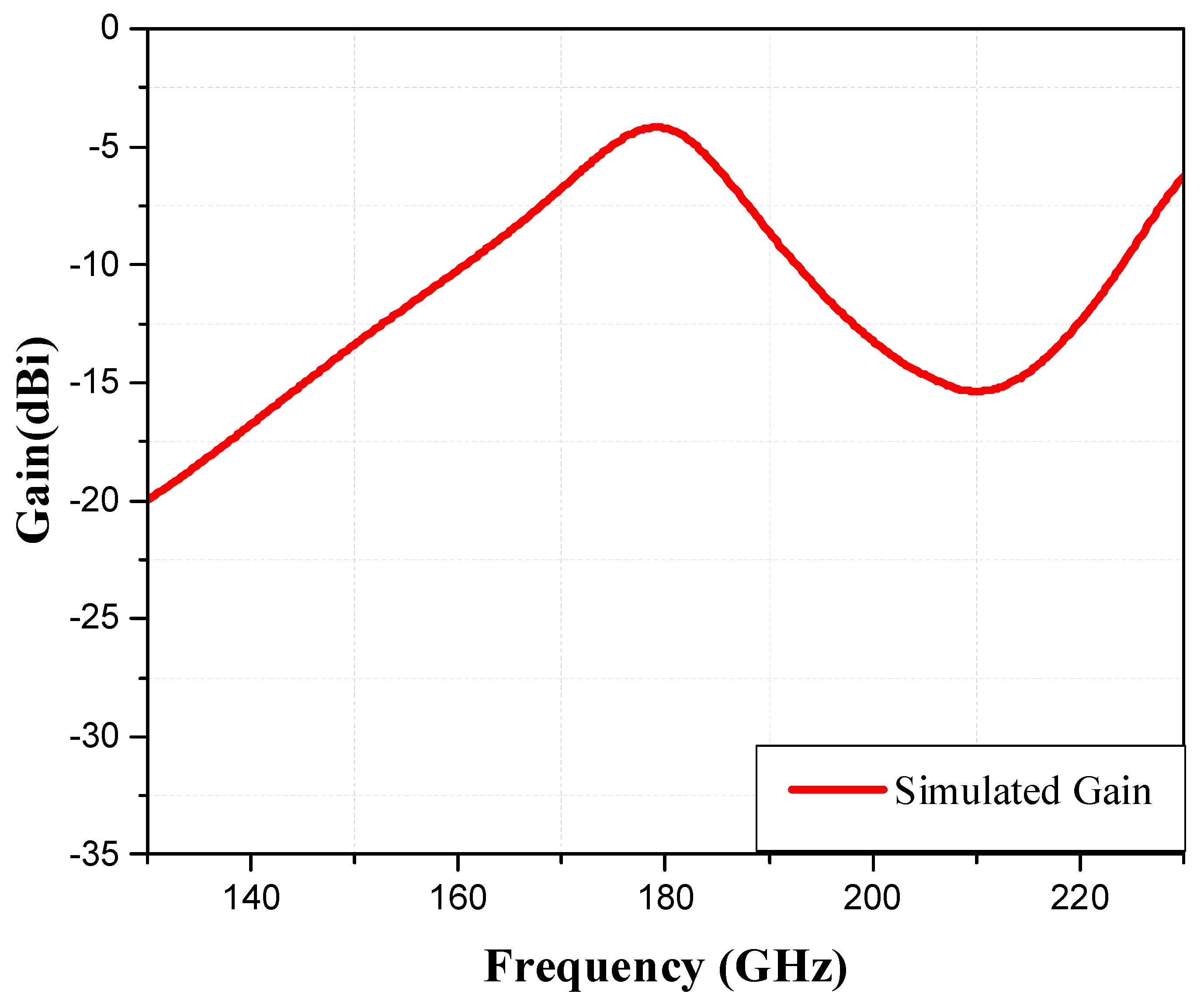
3.4. Gain
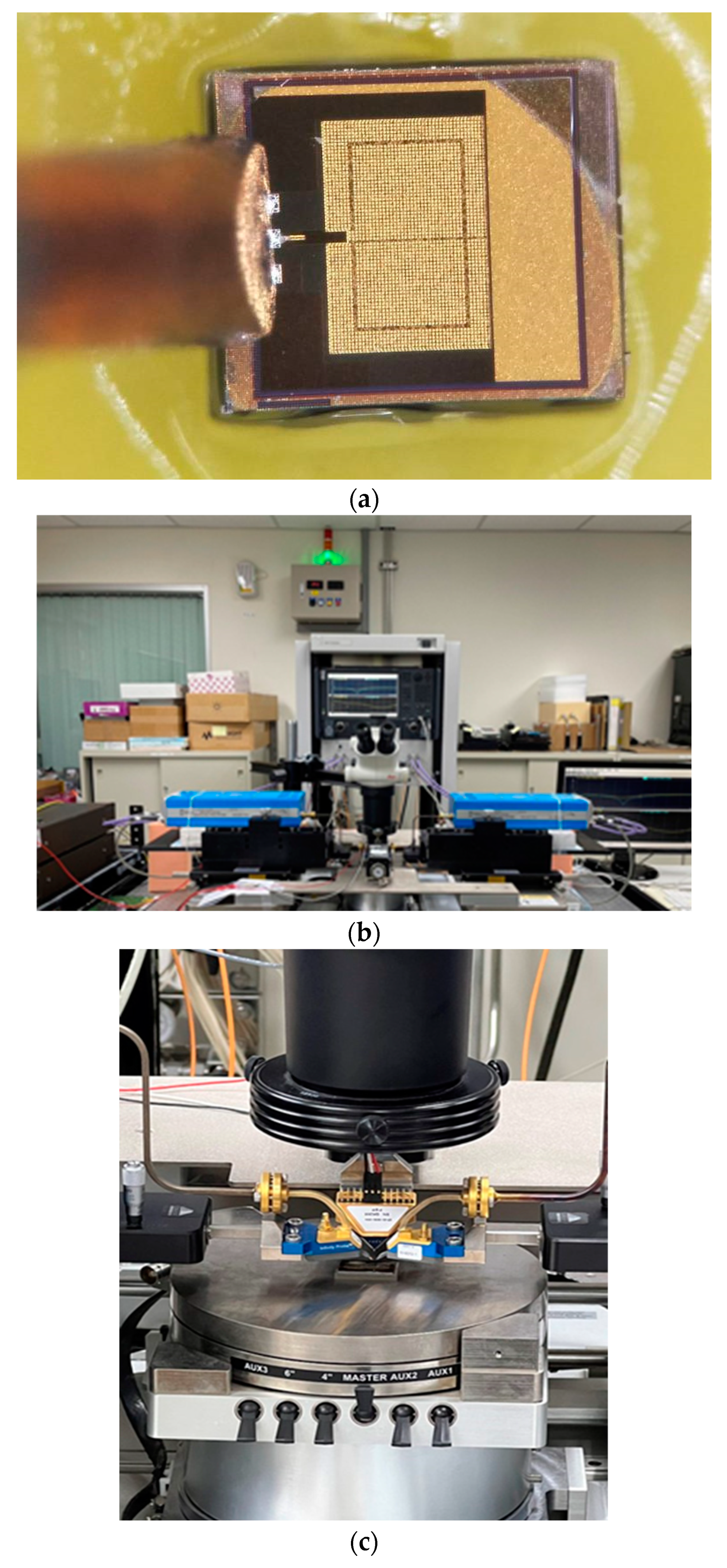
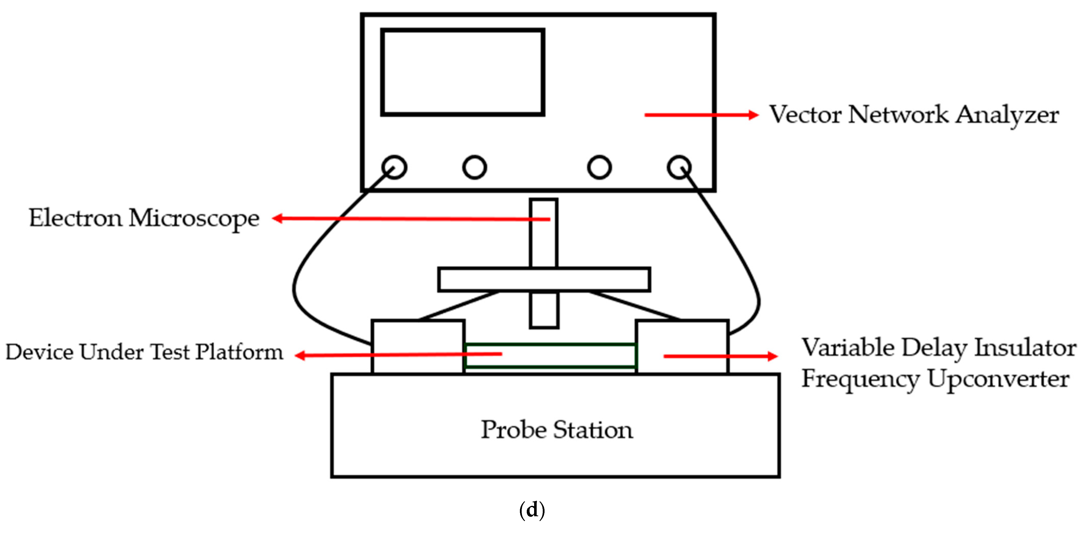
3.5. Prototype and Measurement Environment
3.6. Discuss
3.7. Future Outlook
4. Conclusions
Author Contributions
Funding
Data Availability Statement
Acknowledgments
Conflicts of Interest
References
- Ooms, S.; Reynaert, P. Design and packaging of a robust 120-GHz OOK receiver used in a short-range dielectric fiber link. IEEE Solid-State Circuits Lett. 2020, 3, 42–45. [Google Scholar] [CrossRef]
- Le Zhang, Q.; Chen, B.J.; Chan, K.F.; Chan, C.H. High-gain millimeter-wave antennas based on spoof surface plasmon polaritons. IEEE Trans. Antennas Propag. 2020, 68, 4320–4331. [Google Scholar] [CrossRef]
- Wang, C.; Zhang, N.; Liu, C.; Ma, B.; Zhang, K.; Li, R.; Wang, Q.; Zhang, S. New Advances in Antenna Design toward Wearable Devices Based on Nanomaterials. Biosensors 2024, 14, 35. [Google Scholar] [CrossRef] [PubMed]
- Dey, U.; Hesselbarth, J. Spherical dielectric resonator antenna operating at 180 GHz. IEEE Antennas Wirel. Propag. Lett. 2020, 19, 1380–1384. [Google Scholar] [CrossRef]
- Lammert, V.; Leyrer, M.; Hamouda, M.; Weigel, R.; Issakov, V. Dual-Mode Substrate Wave Cancellation in a 120 GHz 2× 2 On-Chip Dipole Array. IEEE Trans. Antennas Propag. 2022, 70, 6683–6691. [Google Scholar] [CrossRef]
- Cheema, H.M.; Shamim, A. The last barrier: On-chip antennas. IEEE Microw. Mag. 2013, 14, 79–91. [Google Scholar] [CrossRef]
- Kwon, O.-Y.; Cui, C.; Kim, J.-S.; Park, J.-H.; Song, R.; Kim, B.-S. A compact integration of a 77 GHz FMCW radar system using CMOS transmitter and receiver adopting on-chip monopole feeder. IEEE Access 2019, 7, 6746–6757. [Google Scholar] [CrossRef]
- Kong, S.; Shum, K.M.; Yang, C.; Gao, L.; Chan, C.H. Wide impedance-bandwidth and gain-bandwidth terahertz on-chip antenna with chip-integrated dielectric resonator. IEEE Trans. Antennas Propag. 2021, 69, 4269–4278. [Google Scholar] [CrossRef]
- Li, D.-Y.; Jiao, Y.-C.; Yu, H.-W.; Weng, Z.-B. Wideband circularly polarized pyramidal horn antenna based on spoof surface plasmon polaritons. IEEE Trans. Antennas Propag. 2020, 69, 2353–2358. [Google Scholar] [CrossRef]
- Gong, L.; Fu, Y.; Chan, K.Y.; Nanzer, J.A.; Ramer, R. An SIW horn antenna fed by a coupled mode emulating pyramidal horn antennas. IEEE Trans. Antennas Propag. 2019, 68, 33–42. [Google Scholar] [CrossRef]
- Cheng, Y.; Dong, Y. High-Gain All-Metal 3-D Printed Lens–Horn Antenna for Millimeter-Wave Applications. IEEE Antennas Wirel. Propag. Lett. 2022, 22, 308–312. [Google Scholar] [CrossRef]
- Sifat, S.M.; Shams, S.I.; Kishk, A.A. Ka-band integrated multilayer pyramidal horn antenna excited by substrate-integrated gap waveguide. IEEE Trans. Antennas Propag. 2021, 70, 4842–4847. [Google Scholar] [CrossRef]
- He, Y.; Zhao, X.; Zhao, L.; Fan, Z.; Wang, J.-K.; Zhang, L.; Ni, C.; Wu, W.-J. Design of Broadband Double-Ridge Horn Antenna for Millimeter-Wave Applications. IEEE Access 2021, 9, 118919–118926. [Google Scholar] [CrossRef]
- Zhang, Y.; Deng, J.-Y.; Sun, D.; Yin, J.-Y.; Guo, L.-X. Compact slow-wave SIW H-plane horn antenna with increased gain for vehicular millimeter wave communication. IEEE Trans. Veh. Technol. 2021, 70, 7289–7293. [Google Scholar] [CrossRef]
- Chiang, C.-W.; Huang, R.; Liang, C.-J.; Wu, C.-T.M.; Kuan, Y.-C. A 3-D pillar-based electromagnetic interference shield for W-band antenna on silicon using wire bonding technology. IEEE Trans. Compon. Packag. Manuf. Technol. 2021, 11, 2238–2241. [Google Scholar] [CrossRef]
- Chiang, C.-W.; Wu, C.-T.M.; Liu, N.-C.; Liang, C.-J.; Kuan, Y.-C. A Cost-Effective W-Band Antenna-in-Package Using IPD and PCB Technologies. IEEE Trans. Compon. Packag. Manuf. Technol. 2022, 12, 822–827. [Google Scholar] [CrossRef]
- Nafe, M.; Syed, A.; Shamim, A. Gain-enhanced on-chip folded dipole antenna utilizing artificial magnetic conductor at 94 GHz. IEEE Antennas Wirel. Propag. Lett. 2017, 16, 2844–2847. [Google Scholar] [CrossRef]
- Buadana, N.; Jameson, S.; Socher, E. A 280-GHz digitally controlled four port chip-scale dielectric resonator antenna transmitter with DiCAD true time delay. IEEE Solid-State Circuits Lett. 2020, 3, 454–457. [Google Scholar] [CrossRef]
- Choi, S.; Lee, I.; Jeon, S.; Kim, M. 280-GHz Rectangular Cavity Antenna Integrated in an 80-μm InP Substrate. IEEE Antennas Wirel. Propag. Lett. 2016, 16, 837–839. [Google Scholar] [CrossRef]
- Ahmad, W.A.; Kucharski, M.; Di Serio, A.; Ng, H.J.; Waldschmidt, C.; Kissinger, D. Planar highly efficient high-gain 165 GHz on-chip antennas for integrated radar sensors. IEEE Antennas Wirel. Propag. Lett. 2019, 18, 2429–2433. [Google Scholar] [CrossRef]


| Length | Value | Width/Height | Value |
|---|---|---|---|
| L1 | 1200 | W1 | 1200 |
| L2 | 850 | W2 | 850 |
| L3 | 650 | W3 | 450 |
| L4 | 530 | W4 | 325 |
| L5 | 350 | W5 | 190 |
| L6 | 10 | h1 | 533.4 |
| Value (Unit: µm) | Bandwidth (GHz) | Return Loss Lowest Point (dB) |
|---|---|---|
| 10 | 7.77 | −25.4172 |
| 16 | 6.52 | −18.2411 |
| 22 | 5.31 | −14.7682 |
| 28 | 4.35 | −12.9665 |
| 34 | 3.68 | −12.0275 |
| Value (Unit: µm) | Center Frequency (GHz) | Return Loss Lowest Point (dB) |
|---|---|---|
| 455 | 180.99 | −25.4172 |
| 475 | 174.61 | −18.2411 |
| 480 | 173.09 | −14.7682 |
| References | Process | Frequency (GHz) | * FBW (%) | Dimension (mm2) |
|---|---|---|---|---|
| [15] | Wire bonding | 93.7 | 3.8% | 2.1 × 2.1 |
| [16] | IPD | 94.5 | 2% | 1.9 × 1.9 |
| [17] | CMOS | 94.5 | 10.5% | 2.4 × 2.4 |
| [18] | 65 nm CMOS | 280 | *N/A | 2.8 × 2.8 |
| [19] | TSV | 275 | 3.6% | *N/A |
| [20] | 130 nm CMOS | 165 | 5.2% | 1.88 × 1.88 |
| Proposed | SiGe CMOS | 180 | 4.2% | 0.85 × 0.85 |
Disclaimer/Publisher’s Note: The statements, opinions and data contained in all publications are solely those of the individual author(s) and contributor(s) and not of MDPI and/or the editor(s). MDPI and/or the editor(s) disclaim responsibility for any injury to people or property resulting from any ideas, methods, instructions or products referred to in the content. |
© 2024 by the authors. Licensee MDPI, Basel, Switzerland. This article is an open access article distributed under the terms and conditions of the Creative Commons Attribution (CC BY) license (https://creativecommons.org/licenses/by/4.0/).
Share and Cite
Chung, M.-A.; Huang, Z.-Y.; Chen, Y.-H. Horn Antenna on Chip Operating at 180 GHz Using the SiGe CMOS Process. Telecom 2024, 5, 296-311. https://doi.org/10.3390/telecom5020015
Chung M-A, Huang Z-Y, Chen Y-H. Horn Antenna on Chip Operating at 180 GHz Using the SiGe CMOS Process. Telecom. 2024; 5(2):296-311. https://doi.org/10.3390/telecom5020015
Chicago/Turabian StyleChung, Ming-An, Zi-Yu Huang, and Yu-Hsun Chen. 2024. "Horn Antenna on Chip Operating at 180 GHz Using the SiGe CMOS Process" Telecom 5, no. 2: 296-311. https://doi.org/10.3390/telecom5020015
APA StyleChung, M.-A., Huang, Z.-Y., & Chen, Y.-H. (2024). Horn Antenna on Chip Operating at 180 GHz Using the SiGe CMOS Process. Telecom, 5(2), 296-311. https://doi.org/10.3390/telecom5020015