1. Introduction
Data acquisition is an essential part of modern-day signal processing applications in the domains of Industry 4.0 and cyber–physical systems (CPSs).
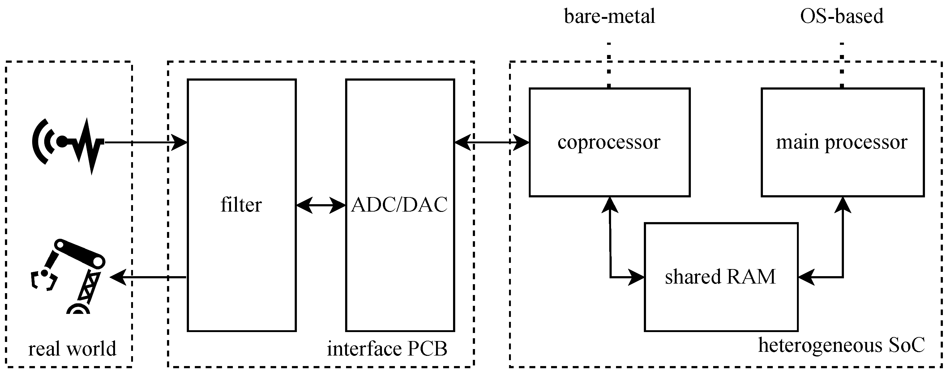
Figure 1 presents the necessary components for a signal processing system. In these types of applications, sensor data originating from various sensing sources need to be digitized at high speeds of sometimes up to the MHz range [
1,
2,
3,
4,
5,
6], with 8- to 32-bit quantization and on multiple channels simultaneously. In these cases, robust and stable sampling is crucial for the validity and performance of the subsequent signal processing steps.
After the digitization step, relevant information is extracted from these signals, e.g., finding specific locations on a captured signal through matched filtering algorithms. After information extraction and decision-making, actuation might have to be performed through one or more digital-to-analog converters (DACs) with similar requirements as the analog-to-digital converters (ADCs).
For prototyping purposes, off-the-shelf solutions exist in the form of specific data-acquisition devices. However, these devices lack processing capabilities and, therefore, require a separate PC to operate and process the acquired data. Another technique used in the design and testing stages of complex real-time embedded systems is hardware-in-the-loop (HiL) simulation with, e.g., a Speedgoat device [
4]. Beyond the prototyping stages, both approaches become too expensive for deployment in the field for real-world applications.
After the prototyping stage, engineers (typically) develop custom-made systems using embedded processors and/or FPGAs and discrete ADCs and DACs. The downside is that this requires significant engineering effort and domain expertise that is not always available in companies that develop Industry 4.0 and CPS solutions. The custom-made solutions make sense for high-volume, low-cost applications, where the engineering effort can be amortized over many individual units. However, in other applications, this is not a viable option.
In traditional embedded designs, a choice is to be made between an operating-system based (OS-based) system and a bare-metal approach. When using OS-based systems, hard real-time requirements for high-performance signal acquisition and actuation will prove very hard to meet. Bare-metal systems are better suited for timing control purposes, but come with an increase in programming effort and a decrease in flexibility and standard functionality. Using heterogeneous systems that consist of both a bare-metal and an OS-based system offer the best of both worlds, allowing strict hard real-time behavior, as well as high flexibility (as explained in more detail in
Section 2.1).
Low-cost open-source systems are available for experimentation with heterogeneous platforms. This takes away part of the hardware design effort. However, it does not eliminate the software engineering effort. This effort is still significant since it requires in-depth knowledge of the system and its possibilities, as programming heterogeneous systems is not straightforward at all.
As mentioned above, the use of a system-on-a-chip (SoC) removes part of the hardware design effort. However, a separate PCB still has to be designed to combine the selected ADC and/or DAC (including appropriate sampling or reconstruction filtering) with the SoC. The SoC controls the interface with the ADC and DAC according to the timing diagrams necessary for the ADC sampling and/or DAC actuation. This requires an exact timing specific to the chosen ADC/DAC. This is typically performed using assembler code in order to have full control over the execution time. This code needs to be written with exact hardware-specific knowledge (e.g., processor and peripheral clock speeds). The data coming from the ADC or going to the DAC can be transferred the main and coprocessor processor using shared RAM.
Having the data available to the main processor, without loading this main processor with the signal acquisition, opens up many opportunities. The main processor can now perform signal processing with more relaxed scheduling deadlines and more processing time available and take care of connectivity and data transfer. This implies that the system can be connected to other computers or “the cloud”, with no further implications on the timing requirements of the ADC/DAC, since this is handled on a separate processor. This connectivity enables remote monitoring and control, as well as combining the unit in a network of measurement and control units, permitting system operation suitable for Industry 4.0 applications such as a complex production line.
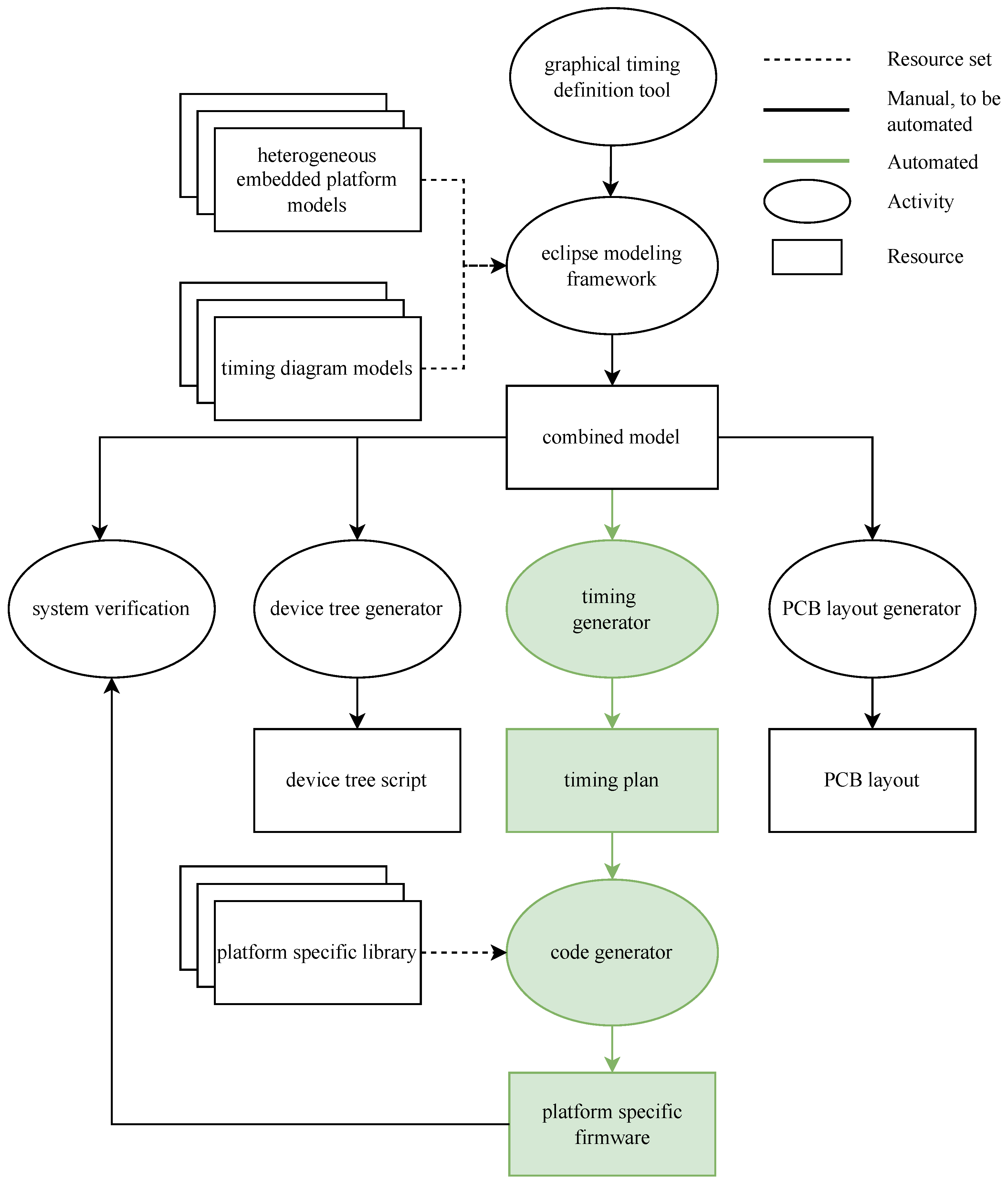
The main objective of this research is to develop a modular high-level toolchain for the development of control systems implemented on heterogeneous platforms, without requiring deep insights from the user into the system’s intricate details. This approach could drastically simplify and speed up the development flow for such systems. Part of the current development complexity lies in the required skillset to develop a full system, since it currently requires expert skills in several domains, e.g., signal processing, embedded software, and hardware design. The focus of this paper is on a model-based code generator, for which the workflow is presented in
Figure 2. The current state-of-the-art is analyzed in
Section 2. An in-depth explanation of the presented work is presented in
Section 3. An evaluation of the developed framework can be found in
Section 4, followed by proposals for future work in
Section 5, and finally, a conclusion on the presented work in
Section 6.
2. State-of-the-Art
2.1. Heterogeneous Systems
With the advances in multi-core processors, as well as programmable hardware for prototyping, the development of heterogeneous embedded systems has become much more feasible and realistic [
7]. Heterogeneous distributed computing systems (HeDCSs) can be described as a collection of diversely capable processors. HeDCSs are an appropriate method for solving computationally intensive problems with a high level of parallelism, as well as a significant diversity between the processes.
Heterogeneity can be presented in two types: performance-level heterogeneity and function-level heterogeneity [
8]. Performance-level heterogeneous systems contain several interconnected similar or identical general-purpose processors of varying speeds. In these systems, a task can be executed by any one of the processors. To achieve function-level heterogeneity, systems combine general-purpose processors with special-purpose processors, such as vector units, floating-point coprocessors, and input/output processors.
The latter combination currently exists in the form of field programmable gate arrays (FPGAs) with soft-core CPUs, e.g., a Xilinx Spartan 6 FPGA combined with a MicroBlaze soft CPU, as an FPGA SoC using FPGA fabric and an ARM processor (e.g., Xilinx’ Zynq series or Intel/Altera’s Cyclone series), or as an SoC such as, e.g., the TI Sitara processor family. A member of the latter family—the AM355x—is currently implemented in the Beaglebone Black SoC [
9]. The interesting part of this architecture is that it combines a high-performance ARM A8 CPU with a low-level programmable real-time unit (PRU-ICSS), i.e., a set of two RISC coprocessors running at 200 MHz with single-instruction I/O capabilities. The coprocessors can be used in combination with the ARM A8 CPU using a shared part of the DDR memory.
Together with the evolution in multi-core solutions, which is mainly focused on increasing the average computing speed, a need for asymmetric multiprocessing has emerged to be able to deal with the non-deterministic and unpredictable time delays specific to scheduling-based systems. This is mainly caused by the very nature of asynchronous events. To understand the problem, a distinction must be made based on the real-time nature of the preferred system. This is divided into three categories, soft, hard, and “on-the-clock true”. The main difference between those categories is the tolerance on the processing time. When looking at soft real-time systems, the response time requirements are often high. However, they are not stringent. A delayed operation due to a rarely occurring peak load can be tolerated. Thus, the system is allowed to delay the response time. For hard real-time systems, the response time requirements are strict deadlines and can result in system failure if not met. The peak load performance must be predictable and should not cause the system to violate the predefined deadlines. Temporal accuracy regarding sequences of events and timing deadlines is often the concern here. A hard real-time system must remain synchronous with the state of the environment in all cases. For industrial use, the use-case of hard real-time systems is more common. However, a further level can be distinguished in the case of hard real-time systems. Some applications have a very narrow or absolutely zero timing tolerance. Such “on-the-clock true” real-time systems are impossible to program on an OS-based system due to the inherent uncertainty in execution time and order, as introduced by the (dynamic) scheduler. Delivering the response too early, which is rarely a problem in common hard real-time systems, is not an event that can be allowed here. Therefore, an exact knowledge of the execution time is necessary, making bare-metal programming essential.
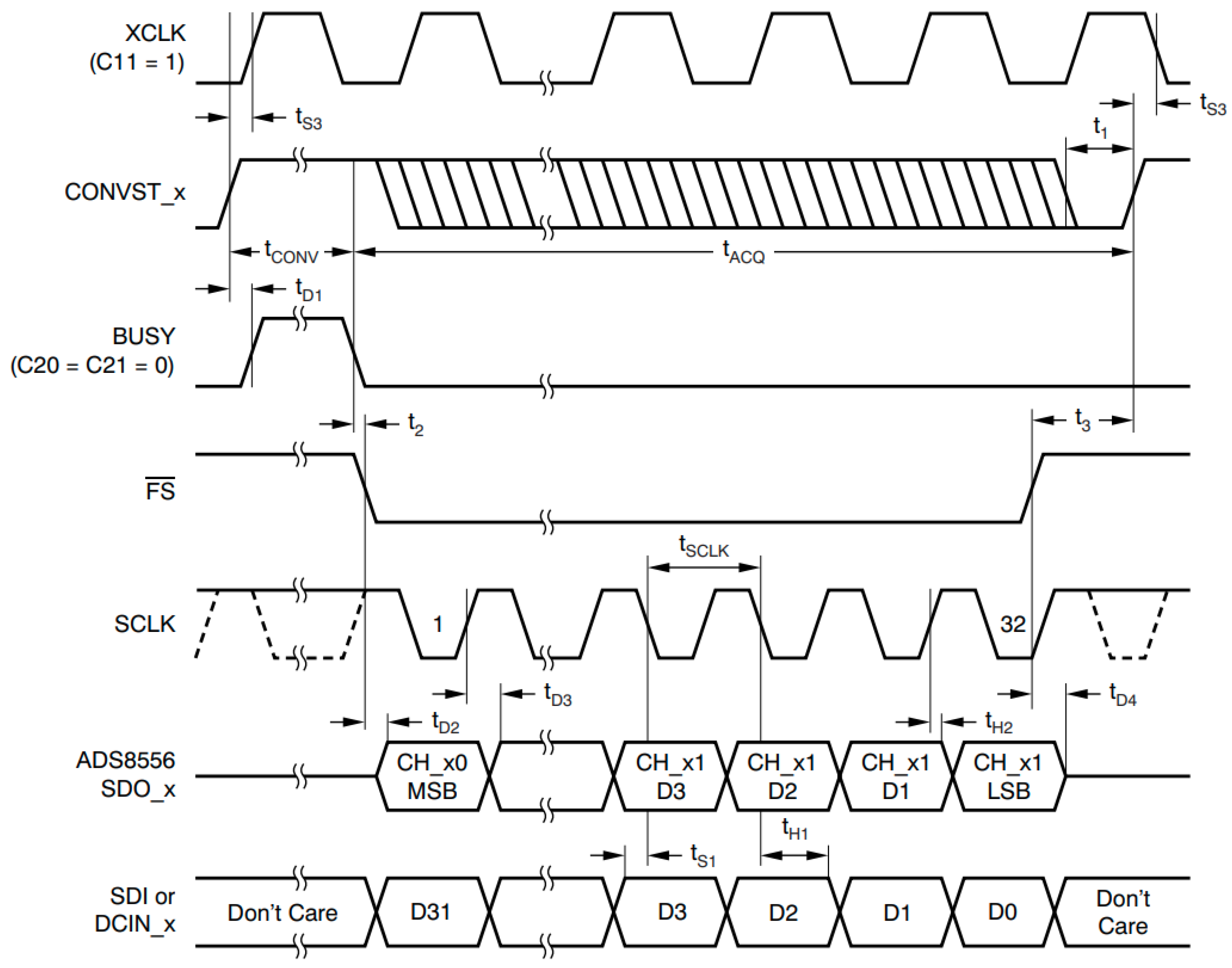
A typical use-case of such a system is the implementation of a timing diagram in the frame of data acquisition or actuation or telecommunication front-ends. An example of such a timing diagram is presented in
Figure 3. Each time interval indicated on the diagram has a specified maximum or minimum value constraint or, sometimes, both. Not meeting these constraints may cause a glitch in the proper operation of the peripheral or might even render it totally dysfunctional. In addition, any jitter on the control clock of the peripheral will negatively effect the treated signals, in the case of an ADC/DAC reducing the effective number of bits (ENOB) of the acquisition/actuation. This level of real-time behavior sets very high requirements for the controlling system, especially when combining this with other functionalities. Being able to use a dedicated core (e.g., one of the coprocessors of the PRU-ICSS on the Beaglebone Black) to control these timings provides a feasible solution.
2.2. Scheduling
The heterogeneity is manifested not only at the hardware and communication protocol level, but also at the level of the scheduling policies used [
11]. Scheduling policies are categorized as static and dynamic. In static scheduling, the execution time, complexity, and data dependencies between the tasks to schedule are known in advance. In dynamic scheduling, tasks are allocated to processors upon arrival, and scheduling decisions must be made during runtime. Task scheduling problems include, e.g., assignment of the appropriate tasks to a suitable processor and ordering of task execution on each resource. Scheduling decisions are based on dynamic parameters, which may change during runtime. Tasks may be reallocated to other processors during runtime. This implies that dynamic scheduling offers the flexibility needed for more complex systems. The combination of static and dynamic scheduling policies can be found on the aforementioned AM335x when it runs GNU/Linux with a priority-driven scheduling algorithm on the main core, whereas the coprocessors are running bare-metal with a static scheduling algorithm. To achieve higher performance, the scheduling efficiency of application tasks is necessary.
2.3. Development Effort Requiring Advanced Tool Support
While the heterogeneous multi-core architectures seem promising, the development effort increases with the level of heterogeneity. This necessitates complex toolchains and programming processes to be able to exploit the full potential of such systems, e.g., the EU-funded ARGO project [
12,
13,
14], which focuses on a worst-case execution-time (WCET)-aware parallel programming model for multi-core architectures in order to enhance predictability. The ARGO project uses a similar approach as the one proposed. A model-based design environment is developed, which enables the developer to design a system from a high-level point of view. Code generation and code transformation are performed with the strong objective of keeping the code base predictable and alarming the developer as soon as possible about problems concerning WCET estimates in the design. The targeted architecture is defined using the Architecture Description Language (ADL). Specific low-level transformations ensure that the WCET constraints are met as muchas possible. In our proposed system, the analyzer is replaced with an analysis of the “on-the-clock true” behavior of the generated code. Another good example of the evolution towards model-based toolchains is found in the work of Gomes et al. [
15], in which a workflow was developed using a model-based approach to port hardware-specific code between different platforms.
Currently, SoC manufacturers appear a bit hesitant about the mentioned model-based approaches. The development environments offered by TI, STMicroelectronics, and NXP remain largely focused on the traditional approach of manual coding [
16,
17]. Their custom tooling does offer some level of automation, in the form of a pin assignment tool and the generation of a device tree script. However, there does not seem to be a good consensus on what the best approach is for this automation. This leads to a variety in the resources brought forth by the manufacturer-specific tooling, leading to cumbersome development effort when switching a developed project between SoCs from different manufacturers.
A good example of just how elaborate the manual development of these resources is can be found in the work of Verreycken et al. [
2]. A system for passive acoustic sound source localization in 3D was developed using a distributed microphone array. For acoustic localization, the main feature to be used is the arrival time of the sound. This creates a need for microphone arrays that are synchronized within a small fraction of the signals’ phase. The microphones are sampled using a single, simultaneously sampling ADC, which results in time synchronization between the microphone channels up to a small fraction of the signal’s phase according to the distance between the microphones. For this specific use-case, the microphone data have to be captured at 285 kHz, at a resolution of 16 bit. Thus, accounting for six channels, the total data throughput is 3.34 MBps per node. The system is based on a Beaglebone Black single-board computer (SBC) extended with a custom PCB, which embeds closely placed microphones, a filtering circuit, and a suitable ADC. To ensure that the data are captured at a correct sampling rate without glitches, low-level interfacing with the ADC is necessary at a precise rate with a real-time processor. The coprocessor (of the Sitara/BBB) runs this assembly program bare-metal and can, therefore, guarantee an exact timing execution at a sufficient data rate to deal with the relatively high data throughput of 3.34 MBps. Higher-level interfacing, such as data transfer, can be handled by the main processor, which is running GNU/Linux.
Directed towards heterogeneous system exploration, this system has been extended in the scope of this paper. The single-capture mechanism was improved by means of a ring buffer for the measurement data, allowing continuous measurements. The ring buffer is shared between the coprocessor and the main processor, allowing the coprocessor to store the data in the buffer, whilst the main core processes and stores or transmits the data for further downstream processing. The only requirement is to process the data fast enough to prevent buffer overwrites. In order to validate this, a TCP connection was set up with a server PC receiving and storing the data coming from the continuously measuring Beaglebone Black setup.
The elaboration of these resources requires a considerable manual engineering effort combined with a vast amount of domain-specific knowledge. The evaluation of these resources allowed bringing forth a separation of the generic and specific parts. This separation leads to the assumption that a generic framework with minimal platform-specific components is possible.
3. Code Generation for a Heterogeneous Platform
Current approaches for the generation of code for a heterogeneous platform are largely based on manual coding, which is arduous and error-prone. This research proposes to autogenerate firmware, based on the model presented in
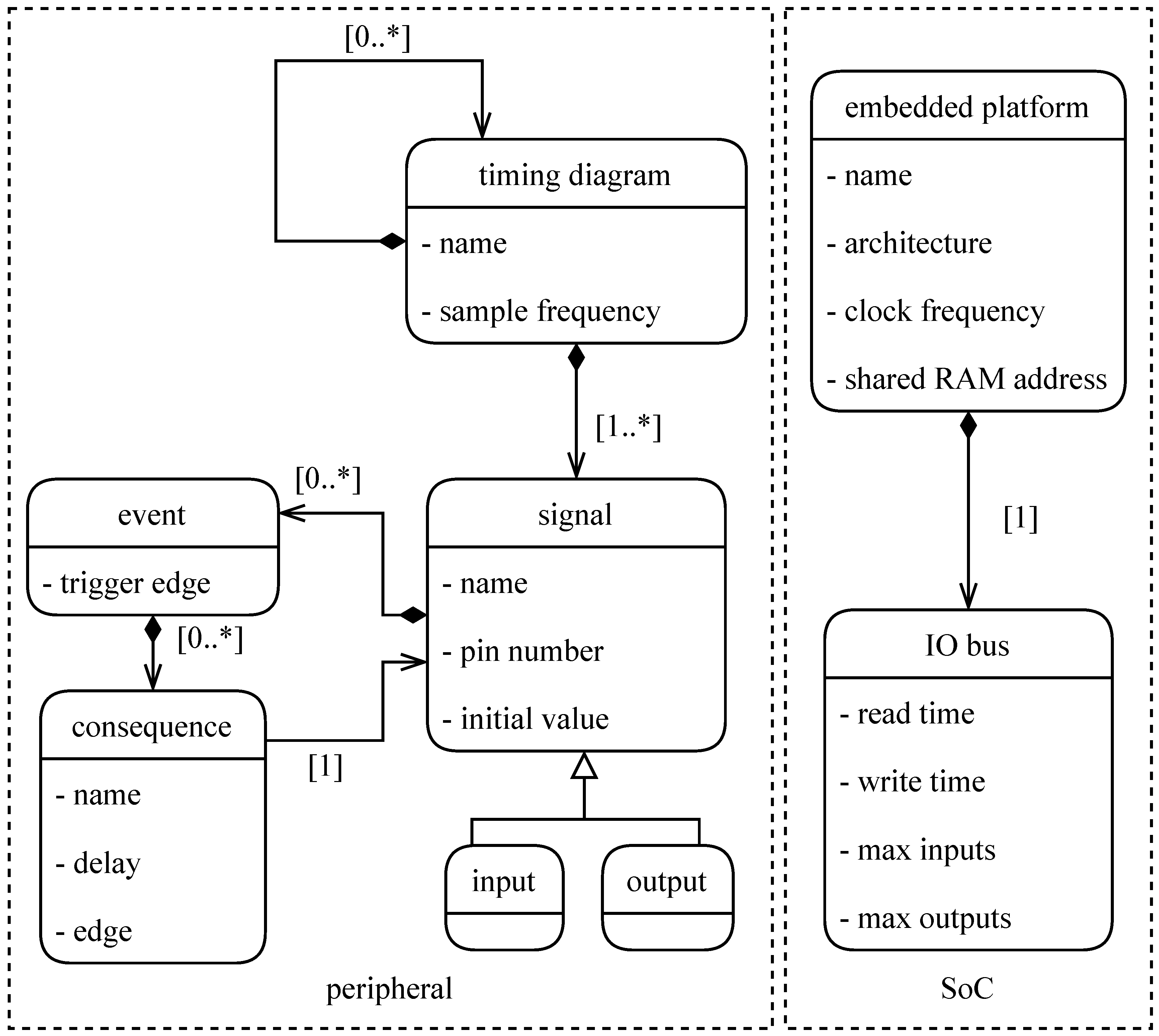
Figure 4, which combines the two main factors that determine the necessary actions. Firstly, the firmware needs to comply with the strictly specified timing diagrams required by ADCs and DACs. Therefore, a formal representation of a timing diagram was developed. In this model, an event-based chain of consequences can be defined. Secondly, an embedded platform defining the platform specifications is modeled, including, e.g., the I/O write and read function’s duration. Depending on the defined platform, the appropriate platform-specific library is included in the program, consisting of four basic functions, namely an initialization, a pin read, a pin write, and a wait function, as well as the shared memory base address. These four functions have proven sufficient to replicate a timing diagram of a deterministic nature.
Currently, this library has been elaborated for the coprocessors on the TI am335x chipset and for a Cortex M4 processor, which is often used as a coprocessor. The development of this library is a straightforward process, since the necessary functions are standard functions for embedded systems. Due to the use of this platform-specific library, the amount of instructions each function takes (i.e., its timing) is verified only once and implemented in the model.
Figure 4 presents a simplified version of the model’s class diagram. A timing diagram is defined as a sequential chain of consequences linked to a signal, where each consequence has the following parameters: the signal on which it should act, the originating signal’s edge that triggers the event, and the time before this consequence takes place. On top of this, a trigger signal is defined. This is essentially the starting point of a timing diagram. The trigger signal is triggered at the start of the timing diagram and sets in motion the chain of consequences and their corresponding events. To allow a fine-grained modularity and definition of the timing, a timing diagram can trigger another timing diagram. This means that separate useful timing diagram models can be defined as building blocks and combined at will. The complete version of the presented class diagram can be found in the publicly available repository [
18], as well as some elaborated examples.
The next step is a model-to-text transformation. This model-to-text transformation is developed in the Eclipse Modeling Framework (EMF) in combination with Acceleo [
19,
20]. Acceleo is an open-source code-generation tool developed inside of the Eclipse Foundation, implementing the Object Management Group’s Meta-Object Facility (MOF) Model to Text Language (MTL) standard, which uses any EMF-based model to generate any kind of code. This part will further be referred to as the “generator”. This generator transforms the model into two files. The first is a C language program, in which the events defined in the model are sequentially evaluated in combination with the specified platform restrictions. This evaluation validates if the defined timing diagram is feasible on the defined platform. The program starts by evaluating whether the events are not scheduled too close to each other, accounting for the read and write times of the defined events on the specific platform.
Currently, it is assumed that simultaneous read or write actions on different inputs/outputs can be bundled, by using direct I/O registers, which control multiple pins. Of course, this approach has its limitations on the amount of pins that can be used per platform. However, to prove the generator’s functionality, this is currently sufficient. If more I/O registers prove necessary for, e.g., a more complex use-case, the evaluation needs to be expanded to include a sequential placement of events impacting a different I/O register (e.g., a read on two input pins linked to separate input registers). Currently, the evaluation applies sequential placement of concurrent events only in the case of a simultaneous input and output event. Since the generator requires the inputs/outputs to be a single I/O register, the assumption is made that each of these events implies only one function call to a read or write function. Deciding which one comes first is fully compliant with the sequence in which they are defined in the model definition, meaning that if the read event has a write event as a consequence with no delay, the write event is executed directly after the read event. In the cases when a delay is defined for an event, the delay is compared with the duration of the previous function call. If this function call lasts longer than the defined delay, the generation of a timing plan is aborted since the proposed timing cannot be respected.
To enable a timing evaluation of the total sampling period during this process of function placement, an incremental sum of the function call durations is kept. In the case of a simultaneous read/write, the timer is added with both events’ durations; otherwise, it is incremented with the specific function’s duration. This timer will be used at the end of the evaluation to determine the amount of instructions used by the defined timing diagram. This process of sequentially checking the timing between events proceeds up until the last defined event of the timing diagram. Subsequently, it evaluates whether the entire chain of consequences does not exceed the sampling period using the aforementioned incremental sum of function call durations and the defined sampling frequency. If the incremental sum is less than the amount of instructions that fit into the sampling period, the remaining instructions are filled with no operation calls (NOPs), to generate an exact match with the defined sampling period, or a nearest high approximation of the defined sampling frequency, as demonstrated in
Section 4. If both evaluations are valid, a valid solution respecting the defined timing is generated and the generator continues. Otherwise, the generation is aborted and the user is informed about the problematic event. If the generation is completed, this results in a timing plan matching the combined model, as presented in
Figure 2. The second is a platform-specific makefile for the generated C language program. When running this makefile, the timing plan is merged with the platform-specific header files. The merger of the timing plan with the platform-specific header files is basically a replacement of the reads, writes, and NOPs with the appropriate function calls and corresponding pinmask. The makefile then compiles this final C language program with the appropriate compiler and settings for the specified platform. The compiled firmware is then ready for deployment on the target system.
This firmware is combined with a controller program on the main core. This program controls the remote processor using the remoteproc framework. Remoteproc allows different platforms/architectures to control (power on, load firmware, power off) remote processors while abstracting the hardware differences and can, as such, be considered as a generic approach [
21]. After starting the coprocessor, the control program is used to access the shared RAM from the Linux user space. Using this access from the Linux user space, the main processor can take care of the further signal processing and/or data transfer with more relaxed scheduling constraints, whilst the coprocessor guarantees the “on-the-clock-true” sampling.
4. Evaluation of the Generated Code
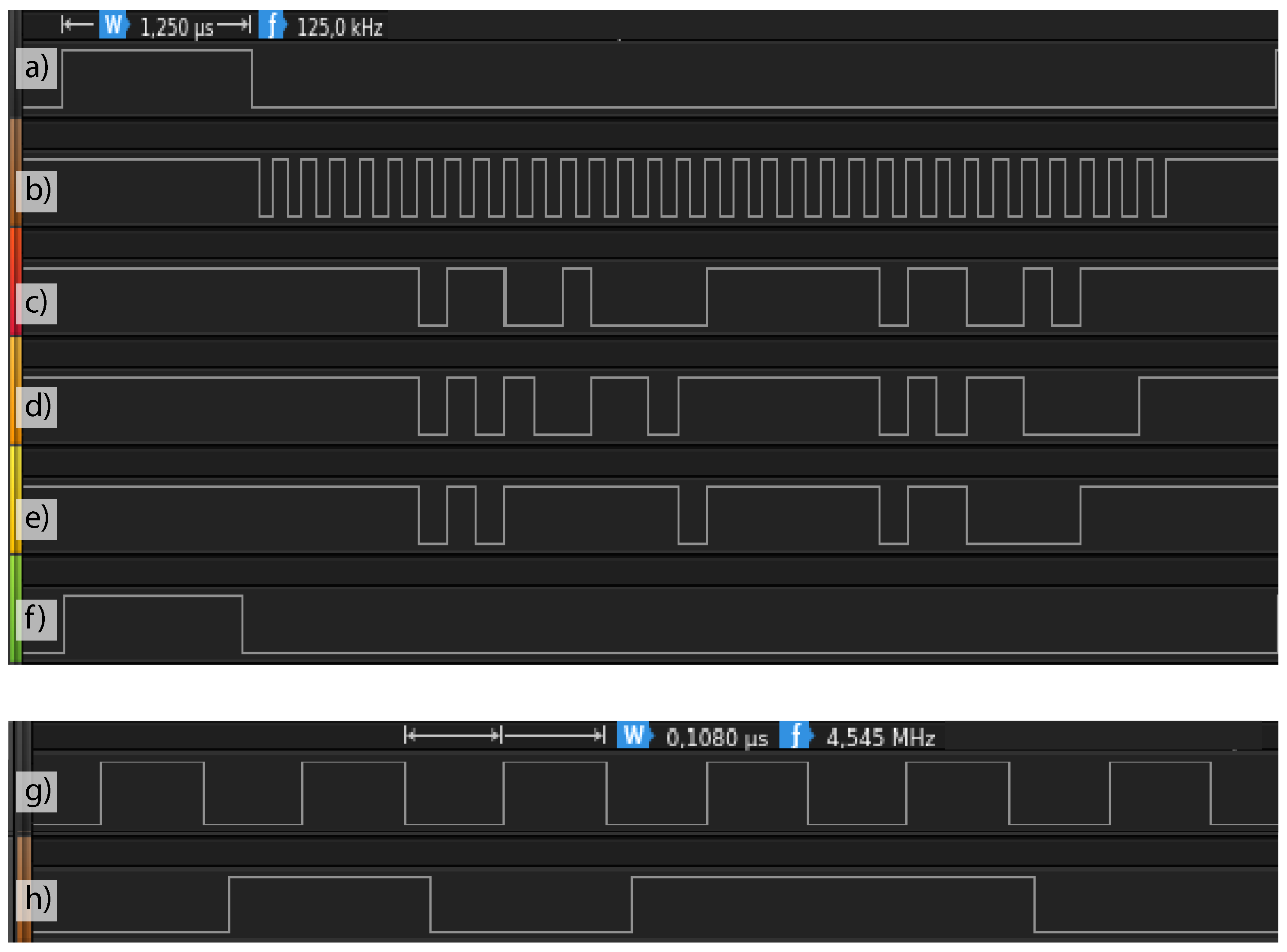
To evaluate the genericity of the framework, two timing diagram examples have been elaborated in combination with a Beaglebone Black and with an STM32MP157DK. First is a timing diagram for six-channel serial operation of the ADS8556 ADC. Second is a timing diagram for three channel pulse-density-modulated (PDM) operation using SPH0641 microphones. When evaluating the timing plan generated from the model, there are three possible outcomes. The first outcome is demonstrated in the top part of
Figure 5. This occurs when the sampling period is an exact multiple of the clock period. In this case, a program that exactly matches the defined sampling frequency can be generated. In the use-case with the ADS8556, the sampling frequency was set to 125 kHz, which is exactly achievable with the 200 MHz clock of the Beaglebone Black’s PRU coprocessor. The second outcome is shown in the bottom part of
Figure 5, where the sampling period is not an exact multiple of this clock period. This implies that the sampling frequency as defined is not possible on the defined platform. In the current implementation, 4.5 MHz was defined, which is not exactly achievable with 200 MHz. The timing plan is then generated for the closest possible higher approximation of the sampling frequency, being 4.545 MHz, whilst informing the user on the adjusted sampling frequency. Most of the time, the sampling frequency is calculated as a minimum value [
22]. This implies that anything higher than the defined sampling frequency is equally adequate, as long as the user or the rest of the system is aware of this change. The third outcome leads to an unsuccessful generation. This occurs when the defined timing diagram is impossible on the defined platform at the defined sampling frequency. The elaborated use-cases verify that the timing evaluation algorithm is successful at performing a thorough analysis of the modeled timing diagram’s implementation feasibility. By covering error conditions, as well as proposing a best fit if an exact match is not present, this approach leads to reliable “on-the-clock true” firmware generation.
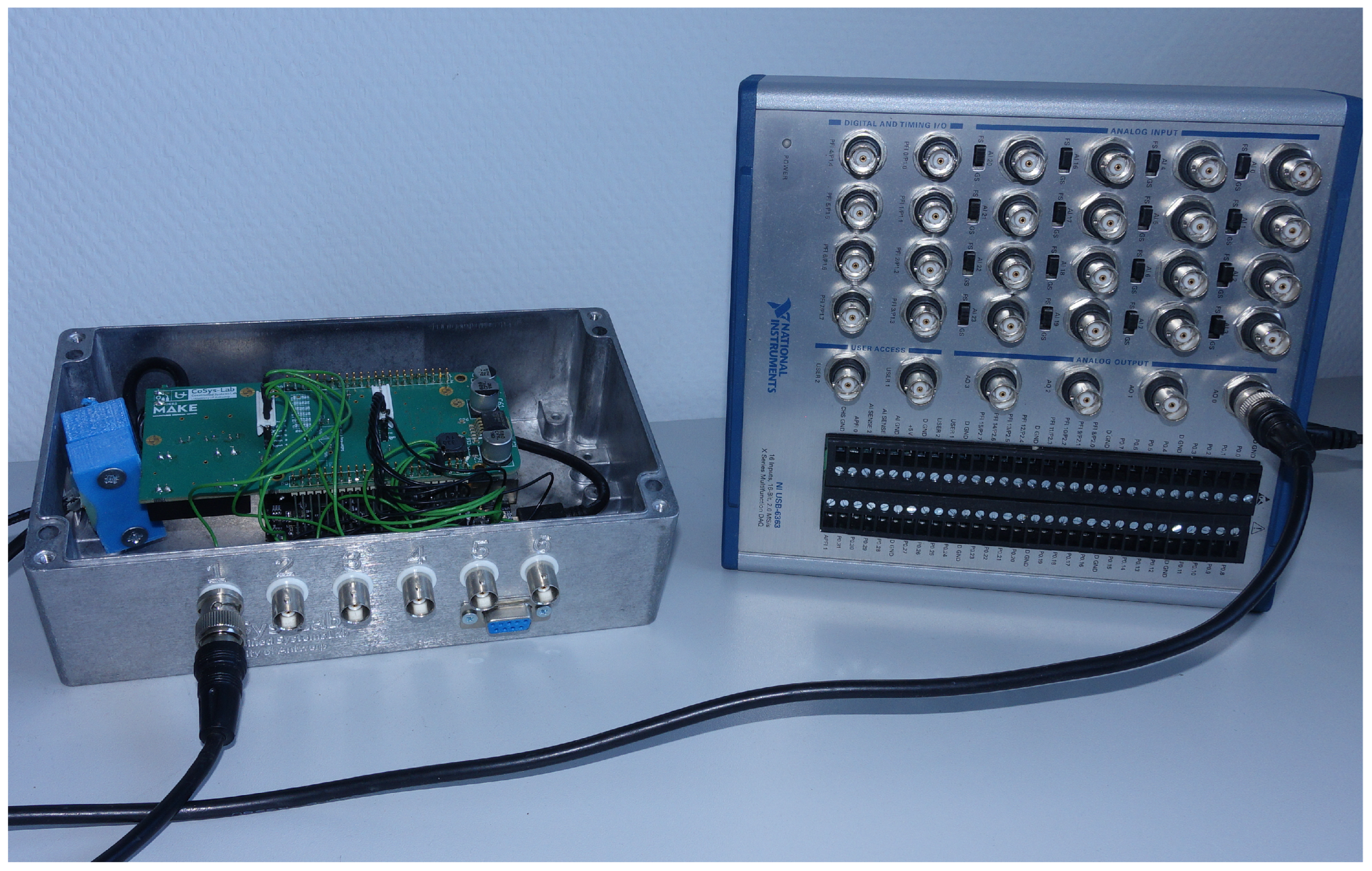
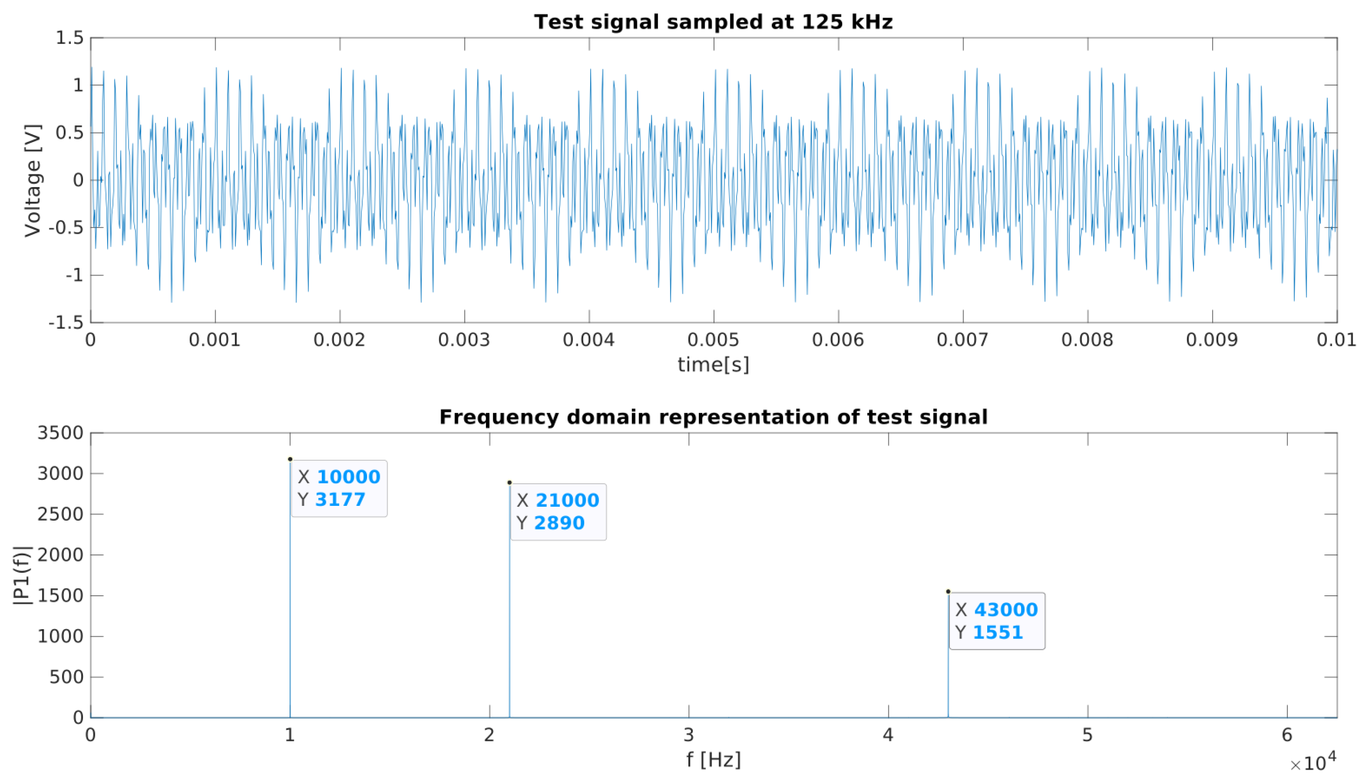
Besides analyzing the generated waveforms to verify that the modeled timing diagram is actually generated, a frequency analysis on a captured test signal was used to prove that the sampling is exact. The test setup is presented in
Figure 6. A test signal is generated using a National Instruments USB-6363 DAQ in combination with Matlab. The generated signal is used as the input to the previously developed hardware (explained in more detail in
Section 2.3). On this setup, the autogenerated firmware is used to sample the test signal at 125 kHz, as defined in the timing diagram model. The generated test signal is a combination of three sine waves with a frequency of 10, 21, and 43 kHz. The exact retrieval of the input signal frequencies in the frequency domain, as demonstrated in
Figure 7, proves that the sampling frequency as defined in the model is exactly achieved, and as such, the firmware can be considered an exact representation of the model’s defined parameters. If the timing was not exact, spurious frequencies or a shift in the peak frequencies would be visible in the frequency analysis [
23]. However, the data from the frequency analysis in
Figure 7 present three clean peaks at the expected locations for the input test signal. To address reusability and modularity, the model was developed with a clear distinction between the timing diagram and the embedded platform. As such, the defined timing diagram for the ADS8556 can easily be recombined with a different platform by loading it into the combined model. To verify this, the embedded platform was replaced with an STM32MP157 instead of the Beaglebone Black. The model definition of both platforms and their implementation in the combined model can be found in [
18].


