Abstract
When using quadrature signals in radio channels, flat and selective fading, multipath radio reception, intersymbol interference, and jitter occur. In addition to the need to accurately estimate the value of the phase difference at the current and previous clock intervals, a critical factor in receiving and demodulating such signals is the accuracy of measuring the amplitude of their samples. When demodulating such signals, an approach is possible, the basis of which is to measure the values of individual signal samples at discrete time points with higher accuracy than in existing electronic devices. Such an approach can be implemented by an optoelectronic device in which a coherent luminous flux is formed, the parameters of which are modulated by a voltage proportional to the readings of the received radio signal. Using a modulated light flux, an interferogram is formed, the parameters of which are directly related to the parameters of this light flux and accordingly to the parameters of the received radio signal. This makes it possible, by increasing the accuracy of estimating radio signal samples, to increase the base of the alphabet used for code manipulation, the efficiency of using the allocated frequency band for transmitting information and reduce the probability of a bit error. The article presents a mathematical model for converting the parameters of the received radio signal into the parameters of the generated interferogram. By mathematical modeling the accuracy characteristics of an optoelectronic device for measuring radio signal samples were evaluated. The results of mathematical modeling illustrating the relationship of the parameters of the optical elements of the device with the accuracy of estimates of the radio signal counts are presented. The practical significance of the proposed optoelectronic device can be used as an independent device for analog-to-digital conversion of radio signals, as well as part of demodulators for QAM and OFDM signals in networks and communication systems of 5G and the next generations.
1. Introduction
The development of information control systems is characterized by a continuous increase in the requirements for the speed of information transmission with a limited frequency band and the power of the transmitted signals. This leads to the widespread use of quadrature (QAM) and OFDM signals [1,2,3,4], which, under the specified limitations, provide a high information transfer rate. This problem manifests itself most significantly in satellite communication and global positioning systems. The creation of robust receivers in GNS systems is associated with the elimination of the influence of a large number of disturbing factors on the reception of such signals [5,6,7,8,9,10,11,12,13,14,15,16,17,18,19,20,21,22,23,24].
To construct demodulators of such signals, devices can be used, the principle of construction of which is based on the use of two reference signals. The phases of these signals are separated by 90°. In addition to, two multipliers and two low-pass filters to form in-phase I and quadrature Q components of the signal are used. Based on the received I and Q components, the amplitude and initial phase of the received signal are determined [25,26,27,28].
However, when demodulating such signals, another approach is possible. The basis of this approach is to measure the values of individual signal samples at discrete time points with higher accuracy than in existing electronic devices. This makes it possible to increase the base of the alphabet used for code manipulation, and the efficiency of using the allocated frequency band to transmit information.
Obtaining high-precision measurements of signal samples allows not only to demodulate signals, but also to measure the signal phase with high accuracy. The latter is necessary in the frequency stabilization method discussed in [29]. In addition, for the practical use of this approach, devices for both measuring samples and demodulating signals, whose frequencies can differ in a wide range, must be unified both in terms of measurement principles and design.
One of the possible approaches to solving these problems is the construction of devices based on the principles of optoelectronics. In accordance with this approach, the purpose of the article is to analyze the possibility of constructing an optoelectronic device that provides measurement of signal samples in a wide frequency range and analysis of its accuracy characteristics.
2. The Principle of Construction and Description of the Device
A possible option for constructing an optoelectronic device for measuring signal samples is based on the principle of controlling the phase of the optical coherent flux. The phase of the flux is changed in accordance with the parameters of the radio signal. This flux is used to form an interferogram. The registration of the interferogram parameters amendment gives the opportunity to measure parameters of radio signal. To control the phase of the optical flux, one of the known optical effects can be used. For example, such electro-optical effect can be realized based on the use an electro-optical modulator (EOM) based on an electro-optical Pokkels cell. Such cell gives the opportunity to change the phase of the light flux according to the law of the received radio frequency oscillation [29,30,31,32]. Currently, in the practical use of EOM, preference is given to devices based on the linear transverse electro-optical effect (EOE), for the implementation of which, as a rule, LiNbO3 material is used as an electro-optical element [33]. The preferred use of LiNbO3 is due to its properties: stable operation of the modulator in a wide temperature range, low energy losses in the optical and microwave ranges, proven technologies for manufacturing structures of optical modulators of this type. In addition, depending on the design of the EOM based on LiNbO3, modulators of this type are high-frequency [33].
In the proposed device, the light flux generated by the laser passes through the EOM and the optical system, falls on the reflective-transmitting Fourier hologram of the holographic interferometer, partially passes through this Fourier hologram and partially diffracts from it [34]. The light flux passing through the Fourier hologram is reflected from a flat mirror, passes in the opposite direction through the Fourier hologram and interferes with the light flux diffracted from the Fourier hologram. As a result of interference, an interferogram is formed in the form of annular interference fringes, the distribution of the intensity of the optical field in the plane of which depends on the refractive index of the EOM material, which varies in accordance with the parameters of the radio signal. The spatial-spectral distribution of the intensity of the optical field in the interferogram plane is recorded by a line of photodetectors with analog-to-digital converters (ADCs) connected to their outputs, performing quantization of signals from the outputs of photodetectors with a discrete step . It should be noted that the value determines the quantization discretion when a radio signal is applied directly to the ADC input.
The block diagram of a holographic optoelectronic radio signal sampling meter using an EOM is shown in Figure 1. The following designations are used in the scheme: 1—a laser with an optical system that provides focusing of the light flux at the point O inside an electro–optical crystal waveguide EOM; 2—an EOM made on the basis of a crystal waveguide made of LiNbO3 material with an optical focusing system of the outgoing light flux with electrodes applied to its surface 3, 3′; 4—Fourier-a hologram of a reflective-transmitting type; 5—a flat mirror; 6—a line of photodetectors with threshold devices connected to their outputs and a device for generating sample values; α—the angle between the plane of the Fourier hologram 4 and the flat mirror 5.
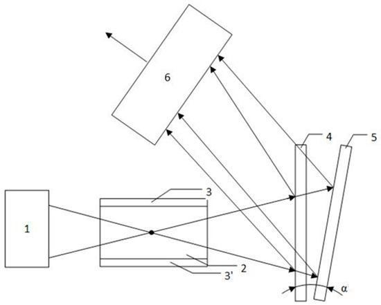
Figure 1.
Block diagram of an optoelectronic device for measuring radio signal samples.
3. Mathematical Model of a Device for Measuring Radio Signal Samples
Expression for the radial intensity distribution the optical field in the plane of the interferogram has the form [34,35,36]:
In expression (1) is the intensity of a constant light background in the interference plane; is the amplitude of the intensity of the interference term of the expression; is the measured coordinate in the plane of the interferogram; is the difference in the path of the rays of two light streams (diffracted from a Fourier hologram and reflected by a flat mirror) in the absence of a signal; is the change in the difference in the course of the rays when the measured signal is applied to the electrodes EOM; is wavelength of optical radiation;
is the angle between the flat mirror and the plane of the Fourier hologram when exposed; is the angle between the flat mirror and the plane of the Fourier hologram when exposed; is the angle between the light beam coinciding with the generatrix of the solid angle limiting the luminous flux incident on the end face of the electro-optical crystal and the normal to this face; —the angle between the direction from the edge of the Fourier hologram to the focus point and the plane of the Fourier hologram; is the distance from the point light source to the Fourier hologram when it is exposed; is the angle that determines the direction of movement of the focus point of the light flux relative to the plane of the Fourier hologram.
Imagine a radio signal, the readings of which need to be measured, at a time in the following form:
In relation (2), the law of change and is determined by the transmitted information and the type of manipulation used.
When a signal (2) is applied to the electrodes 3, 3′, the refractive index of the EOM material changes according to the law:
where is the proportionality coefficient, which determines the change in the refractive index of an electro-optical material under the action of an applied voltage.
When the signal level (2) changes due to a change in the refractive index of the EOM material, the focusing point of the light flux moves by an amount [37,38]
In Formulas (4)–(7), is the linear size of an electro-optical crystal along the optical axis of the light flux passing through this crystal; is the angle of refraction in an electro-optical crystal of an optical beam incident on the end face of this crystal at an angle; is the effective refractive index of the crystal waveguide material is the EOM of the crystal in the absence of voltage on its electrodes; is electro-optical coefficient; is the distance between the electrodes.
Taking into account the optical system that implements the effect of amplifying the phase of the luminous flux with a thin collecting lens, the movement of the focusing point of the luminous flux leads to an increase in the difference in the course of the rays, the value of which will be
where is focal length of the thin lens.
The ratios (1)–(8) allow us to determine the relationship between the parameters of the device in question and the accuracy of measuring the radio signal samples.
4. Evaluation of the Accuracy Characteristics of the Device for Measuring Radio Signal Samples
It follows directly from formula (1) that the change in the intensity level of the optical field in the plane of the interferogram, manifested as a shift of interference fringes in its plane must be estimated at points . The value of shift of interference fringes depends on the parameters of the input radio signal and the dependency has the greatest steepness along the line of photodetectors. Coordinates of the specified points at are determined from the solution of the equation:
In the specified points are shifted by an amount , defined by the expression:
where and denote the derivatives of the corresponding functions.
The specified offset will lead to a change in the intensity of the optical field at the points by the amount of ():
The resulting change can be registered and measured using a photodetector 6, provided that it exceeds the quantization discretion of the ADC. This condition can be written in the form , where is the conversion coefficient of the photodetector. In this case, the quantization error is . Thus, the minimum change of value , which can be registered by the optoelectronic device in question is determined by the expression:
The ratios (4)–(12) allow us to establish a relationship between the quantization step of an optoelectronic device and the discrete step of an ADC, respectively, in the form of:
Thus, the choice of parameters of the optical part of the optoelectronic device , , , , , , , allows you to change the quantization step when evaluating radio signal samples. Of the entire set of these parameters, the parameters and have the greatest impact on the gain in the accuracy of the evaluation. These parameters determine the curvature of the wavefront of the signal light flux when exposing a Fourier hologram. When forming a holographic interferogram, this causes a high sensitivity of the spatial-spectral distribution of the intensity of the optical field to the estimated readings of the received radio signal. At the same time, the value of it should not be too small, since the distance between the interference maxima increases, which leads to an increase in the linear dimensions of the interferogram.
5. Discussion
The simulation was carried out at the following values of the parameters of the optoelectronic device and its components: , , , , .
Figure 2 shows the corresponding variation of the radial distribution of the intensity of the optical field in the plane of the interferogram centered at the point for a moment in time , corresponding to the maximum reference value of the received radio signal.
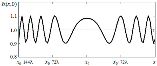
Figure 2.
The radial distribution of the intensity of the optical field in the plane of the interferogram.
The greatest variation of the gain in the accuracy of measuring the parameters of the radio signal, as shown by the analysis of the ratio (13), is associated with the angle and distance . This determines the need for simultaneous analysis of the influence of these two parameters on the gain in the accuracy of the evaluation of the radio signal samples and allows you to determine the range of the specified parameters’ values, the angle and distance, in which a gain in measurement accuracy reaches the greatest value.
In accordance with this, Figure 3 shows a two-dimensional variation of the gain in measurement accuracy from the specified parameters, which determines an increase in the accuracy of measurements of radio signal samples.
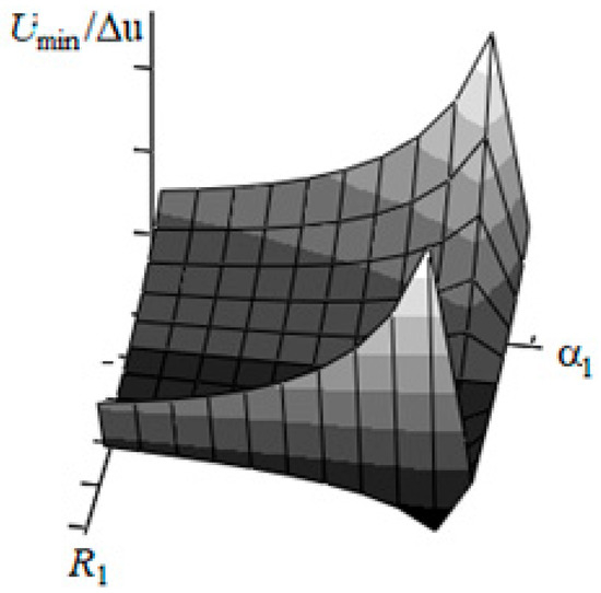
Figure 3.
Two-dimensional variation of the reduction of the ratio of quantization counts of an optoelectronic device and an electronic ADC in and m parameters variations.
As follows from the obtained variation, there is a range of parameter values and , within which the proposed optoelectronic device provides a gain in measurement accuracy.
The corresponding one-dimensional variation of increasing the accuracy of estimating radio signal samples depending on the value of each of these parameters at the optimal value of the second parameter are shown in Figure 4. The parameter value m and the value is 0.00963. This corresponds to a gain in accuracy of evaluation 104 times.
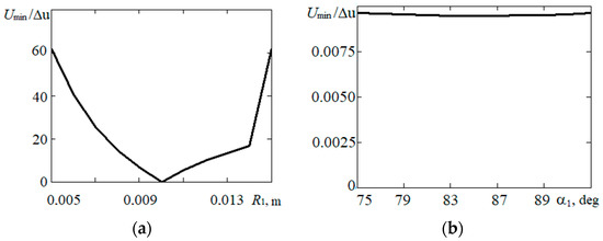
Figure 4.
Variation of the reduction of the ratio of quantization counts of an optoelectronic device and an electronic ADC: (a)—in , variation ; (b)—in variation, m.
During the research, it was also found that the gain in the accuracy of measurements of an optoelectronic device is the same for different orders of interferogram .
6. Conclusions
The article considers a variant of solving the problem of increasing the accuracy of estimating radio signal samples. The proposed solution can be implemented by an optoelectronic device in which a coherent luminous flux is formed. The parameters of the generated light flux are modulated by a voltage proportional to the readings of the received radio signal. Using a modulated light flux, an interferogram is formed, the parameters of which are directly related to the parameters of this light flux, and, accordingly, to the parameters of the received radio signal. The spatial-spectral distribution of the intensity of the optical field in the interference plane is recorded by photodetectors, the signals from the outputs of which are converted into digital form. Analog-to-digital conversion of the received radio signal using an EOM, a holographic interferometer and a group of ADCs placed in the interference bands of the interferogram requires mandatory consideration of the nature of the spatial-spectral distribution of the intensity of the optical field in its plane. The performed analysis showed the relationship between the accuracy of estimating the parameters of the received radio signal and a number of design parameters of an optoelectronic device determined by the characteristics of its optical circuit elements. The choice of parameters of the optical part of the optoelectronic device , , , , , , , , justified by the results of the conducted research, allows to reduce the quantization step when measuring radio signal samples. This leads to an increase in the accuracy of measurements of these samples. The greatest variation of the gain in the accuracy of measuring the parameters of the radio signal, as the research results show, is associated with the angle and distance .
The achieved increase in the accuracy of estimating the radio signal counts makes it possible to increase the base of the alphabet used for code manipulation, the efficiency of using the allocated frequency band for transmitting information and reduce the probability of a bit error.
Author Contributions
Conceptualization, O.A.S., M.Y.Z., A.G.P. and I.A.A.; methodology, O.A.S., A.G.P. and I.A.A.; software, O.A.S., M.Y.Z. and I.A.A.; validation, O.A.S.; formal analysis, O.A.S., M.Y.Z. and A.G.P.; investigation, O.A.S., A.G.P. and M.Y.Z.; resources, I.A.A.; data curation, O.A.S. writing—original draft preparation, O.A.S. and A.G.P.; writing—review and editing, O.A.S. and M.Y.Z.; visualization, O.A.S. and I.A.A.; supervision, O.A.S., M.Y.Z. and A.G.P.; project administration, O.A.S.; funding acquisition, O.A.S. All authors have read and agreed to the published version of the manuscript.
Funding
This research received no external funding.
Institutional Review Board Statement
Not applicable.
Informed Consent Statement
Not applicable.
Data Availability Statement
The study did not report any data.
Acknowledgments
We thank Dmitriy Davidovich Gabrielyan for the help in this research.
Conflicts of Interest
The authors declare no conflict of interest.
References
- Tuovinen, T.; Tervo, N.; Pärssinen, A. Analyzing 5G RF System Performance and Relation to Link Budget for Directive MIMO. IEEE Trans. Antennas Propag. 2017, 65, 6636–6645. [Google Scholar] [CrossRef]
- Taniguchi, R.; Nishimori, K.; Kataoka, R.; Kameyama, K.; Kitao, K.; Tran, N.; Imai, T. Evaluation of massive MIMO considering real propagation characteristics in the 20-GHz Band. IEEE Trans. Antennas Propag. 2017, 2, 6703–6711. [Google Scholar] [CrossRef]
- Tikhvinskiy, V.O. Design features and ems-characteristics of future equipment of 5g mobile communication networks. Telecommun. Radio Eng. 2018, 6, 63–68. [Google Scholar]
- Bakulin, M.G.; Rejeb, T.B.K.; Kreyndelin, V.B.; Mironov, Y.B.; Pankratov, D.Y.; Smirnov, A.E. Modulation for cellular 5G/IMT-2020 and 6G networks. T-Comm 2022, 16, 11–17. [Google Scholar] [CrossRef]
- Wang, Y.C.; Milstein, L.B. Rejection of multiple narrow-band interference in both BPSK and QPSK DS spread-spectrum systems. IEEE Trans. Commun. 1988, 36, 195–204. [Google Scholar] [CrossRef]
- Krishnamurthy, V.; Logothetis, A. Adaptive nonlinear filters for narrow-band interference suppression in spread-spectrum CDMA systems. IEEE Trans. Commun. 1999, 47, 742–753. [Google Scholar] [CrossRef]
- Soderstrand, M.A.; Johnson, L.G.; Phillips, S.R. New technique for attenuation of narrow-band interference with applications in control and communications systems. In Proceedings of the 2006 Fortieth Asilomar Conference on Signals, Systems and Computers, Pacific Grove, CA, USA, 29 October–1 November 2006; pp. 1027–1031. [Google Scholar]
- Gamba, M.T.; Falletti, E. Performance analysis of FLL schemes to track swept jammers in an adaptive notch filter. In Proceedings of the 2018 9th ESA Workshop on Satellite Navigation Technologies and European Workshop on GNSS Signals and Signal Processing (NAVITEC), Noordwijk, The Netherlands, 5–7 December 2018; pp. 1–8. [Google Scholar]
- Gamba, M.T.; Falletti, E. Performance comparison of FLL adaptive notch filters to counter GNSS jamming. In Proceedings of the 2019 International Conference on Localization and GNSS (ICL-GNSS), Nuremberg, Germany, 4–6 June 2019; pp. 1–6. [Google Scholar]
- Kamath, V.; Lai, Y.-C.; Zhu, L.; Urval, S. Empirical mode decomposition and blind source separation methods for antijamming with GPS signals. In Proceedings of the 2006 IEEE/ION Position Location, and Navigation Symposium, Coronado, CA, USA, 25–27 April 2006; pp. 335–341. [Google Scholar]
- Fante, R.L.; Vaccaro, J.J. Wideband cancellation of interference in a GPS receive array. IEEE Trans. Aerosp. Electron. Syst. 2000, 36, 549–564. [Google Scholar] [CrossRef]
- Myrick, W.L.; Goldstein, J.S.; Zoltowski, M.D. Low complexity anti-jam space-time processing for GPS. In Proceedings of the 2001 IEEE International Conference on Acoustics, Speech, and Signal Processing, Proceedings (Cat. No.01CH37221), Salt Lake City, UT, USA, 7–11 May 2001; pp. 2233–2236. [Google Scholar]
- Musumeci, L.; Dovis, F. Use of the wavelet transform for interference detection and mitigation in global navigation satellite systems. Int. J. Navig. Obs. 2014, 2014, 1–14. [Google Scholar] [CrossRef]
- Musumeci, L.; Dovis, F. Performance assessment of wavelet based techniques in mitigating narrow-band interference. In Proceedings of the 2013 International Conference on Localization and GNSS (ICL-GNSS), Turin, Italy, 25–27 June 2013; pp. 1–6. [Google Scholar]
- Daniele, B.; Pau, C. Complex signum non-linearity for robust GNSS interference mitigation. IET Radar Sonar Navig. 2018, 12, 12900–12909. [Google Scholar] [CrossRef]
- Borio, D.; Cano, E. Optimal global navigation satellite system pulse blanking in the presence of signal quantisation. IET Signal Process. 2013, 7, 400–410. [Google Scholar] [CrossRef]
- Kaplan, E.D.; Hegarty, C. Understanding GPS/GNSS: Principles and Applications; Artech House: Norwood, MA, USA, 2017. [Google Scholar]
- Zhang, Y.; Wu, H.; Gao, Y. Transform domain interference suppression in GPS/BD-2 receiver based on fractional Fouriertransforms. In Proceedings of the 26th International Technical Meeting of the Satellite Division of the Institute of Navigation (ION GNSS + 2013), Nashville, TN, USA, 16–20 September 2013; pp. 3456–3463. [Google Scholar]
- Capozza, P.T.; Holland, B.J.; Hopkinson, T.M.; Landrau, R.L. A single-chip narrow-band frequency-domain excisor for a globalpositioning system (GPS) receiver. IEEE J. Solid-State Circuits 2000, 35, 401–411. [Google Scholar] [CrossRef]
- Garzia, F.; van der Merwe, J.R.; Rügamer, A.; Urquijo, S.; Felber, W. HDDM hardware evaluation for robust interference mitigation. Sensors 2020, 20, 6492. [Google Scholar] [CrossRef] [PubMed]
- van der Merwe, J.R.; Garzia, F.; Rügamer, A.; Urquijo, S.; Contreras Franco, D.; Felber, W. Wide-Band Interference Mitigation in GNSS Receivers Using Sub-Band Automatic Gain Control. Sensors 2022, 22, 679. [Google Scholar] [CrossRef] [PubMed]
- Falen, G.L. Analysis and Simulation of Narrowband GPS Jamming Using Digital Excision Temporal Filtering. In Air Force Inst of TechWright-Patterson AFB oh School of Engineering; Wright-Patterson AFB: Green, OH, USA, 1994. [Google Scholar]
- Yousif, T.; Blunt, P. Interference Mitigation for GNSS Receivers Using FFT Excision Filtering Implemented on an FPGA. Engineering 2022, 3, 439–466. [Google Scholar] [CrossRef]
- Ma, S.; Zhang, Z.; Li, H.; Xu, J.; Zhang, H.; Zhang, S.; Li, S. Design of DBN based Demodulator in Underwater Wireless Optical Communications. In Proceedings of the 2020 IEEE/CIC International Conference on Communications in China (ICCC Workshops), Chongqing, China, 9–11 August 2020; pp. 179–184. [Google Scholar] [CrossRef]
- Timofeyev, A.L.; Sultanov, A.K. Influence of Noise and Sampling Rate on the Error of Discrete Image Representation. Inf. Control Syst. 2021, 5, 33–39. [Google Scholar] [CrossRef]
- Jia, J.; Jiang, Y.; Cui, Y. Phase Demodulator for the Measurement of Extrinsic Fabry-Perot Interferometric Sensors With Arbitrary Initial Cavity Length. IEEE Sens. J. 2020, 20, 3621–3626. [Google Scholar] [CrossRef]
- Hou, Y.; Wang, Y.; Wang, H.; Liu, Q.; Li, L.; Li, Z. Research and Implementation of Super High-Speed Fiber Bragg Grating Demodulator. In Proceedings of the 2019 IEEE International Instrumentation and Measurement Technology Conference (I2MTC), Auckland, New Zealand, 20–23 May 2019; pp. 999–1003. [Google Scholar]
- Safaryan, O.A.; Alferova, I.A. Prerequisites and Theoretical Foundations of the Statistical Method of Frequency Stabilization in Information and Telecommunication Systems. Electronics 2022, 11, 2809. [Google Scholar] [CrossRef]
- Fedorov, B.F.; Tsibulkin, L.M. Holography; Radio and Communications: Narita, Japan, 1989; p. 144. [Google Scholar]
- Born, M.; Wolf, E. Principles of Optics; Pergamonrpess: Oxford, UK, 1968; p. 856. [Google Scholar]
- Balakshiy, V.I.; Parygin, V.N.; Chirkov, L.I. Physical Foundations of Acousto-Optics; Peace Publ.: Moscow, Russia, 2000; p. 265. [Google Scholar]
- Parygin, V.N.; Vershubskii, A.V.; Filatova, E.Y. Optimization of the transfer function of an acoustooptic cell with an apodized piezoelectric transducer. Tech. Phys. 2001, 71, 73–78. [Google Scholar] [CrossRef]
- Semenov, A.S.; Smirnov, V.L.; Shmalko, A.V. Integrated Optics for Information Transmission and Processing Systems; Radio and Communications: Moscow, Russia, 1990; p. 224. [Google Scholar]
- Miler, M. Holografie; SNTL: Praha, Czech Republic, 1974; p. 207. [Google Scholar]
- Prygunov, A.G.; Sizov, V.P.; Bezuglov, D.A. Method for object movement determination based on analysis of optical field wavefronts using reference holograms. Atmos. Ocean. Opt. 1995, 8, 826–830. [Google Scholar]
- Bezuglov, D.A.; Prygunov, A.G.; Trepachev, V.V. Analysis of light diffraction on a reference hologram when measuring object displacements by the spatial-spectral method. Autometr 1998, 5, 27–37. [Google Scholar]
- Matveev, A.N. Fundamentals of Optics; Peace Publ.: Moscow, Russia, 1989; p. 685. [Google Scholar]
- Unger, H.-G. Optische Nachrichten Technik; Elitera–Verlag: Berlin, Germany, 1976; p. 264. [Google Scholar]


Disclaimer/Publisher’s Note: The statements, opinions and data contained in all publications are solely those of the individual author(s) and contributor(s) and not of MDPI and/or the editor(s). MDPI and/or the editor(s) disclaim responsibility for any injury to people or property resulting from any ideas, methods, instructions or products referred to in the content. |
© 2023 by the authors. Licensee MDPI, Basel, Switzerland. This article is an open access article distributed under the terms and conditions of the Creative Commons Attribution (CC BY) license (https://creativecommons.org/licenses/by/4.0/).