Proceeding Paper

A Novel PDMS-Based Microfeature-Size Fabrication Method for Biocompatible and Flexible Devices †

by
Fatemeh Mashayekhi
*,
Faezeh Shanehsazzadeh
and
Mehdi Fardmanesh
Department of Electrical Engineering, Sharif University of Technology, Tehran 1458889694, Iran
*
Author to whom correspondence should be addressed.
Presented at the 2nd International Electronic Conference on Applied Sciences, 15–31 October 2021; Available online: https://asec2021.sciforum.net/.
Eng. Proc. 2021, 11(1), 36; https://doi.org/10.3390/ASEC2021-11132
Published: 15 October 2021
(This article belongs to the Proceedings of The 2nd International Electronic Conference on Applied Sciences)

Abstract

:
This article proposes a novel cost-effective method to achieve microfeature-sized patterns on Polydimethylsiloxane (PDMS) substrates. As a biocompatible, flexible, economical, and easy-to-use polymer benefiting the trait of mechanical impedance close to that of soft tissues, PDMS is the best candidate to be used where we need communication between the electrical circuits and soft tissues. Additionally, PDMS can be matched with tissue’s different shapes and doesn’t cause any trauma. The proposed approach eliminates complex and high-cost manufacturing methods of microfeature-sized patterns on PDMS, such as conventional microfabrication methods. Our technique takes advantage of not requiring standard photolithography processes, making it simple and cost-effective. This manner can be used for various purposes, such as micro-fluidic chip fabrication, bio-sensing applications, neuroscience research and neural prosthetics such as electrocorticogram (ECoG) and, in general, where microfeature-size patterning on PDMS is required. To prove the method’s functionality, we fabricated a test sample. Firstly, the scaffold was fabricated using a conventional laser engraver and Poly(methylmethacrylate) (PMMA). Then, a mold was made using this scaffold from PDMS. In the last step, a typical commercial photoresist was applied as an anti-adhesion layer between the PDMS mold and the sample to make the sample peel off the mold surface easily. The final sample indicated that the pattern’s feature size was around 200 micrometers and that the required patterns were very close to the desired form possible.

1. Introduction

Flexible, elastic, and durable soft materials lead the path for future electronics applications in diagnostics and personal healthcare [1]. As a biocompatible, flexible, simple processing, optically transparent, and cost-effective polymer, PDMS (polydimethylsiloxane) is one of the most frequently applied substrate layers [2,3] in various applications including wearable sensors [4,5], epiretinal prosthetics [6,7,8], electronic textiles [9,10], stretchable conductors [11,12], etc. PDMS can be made in different shapes to fit biological tissues. Moreover, its mechanical impedance matching property to soft tissues such as the spinal cord and the oxygen-permeability make it one of the best MEA/neural tissue interfaces [13,14,15]. Other flexible substrate options include parylene-c [16,17], Ecoflex 00-30 [18], silicon elastomers like RTV-2 [19], and so on. PDMS Young’s modulus is reported in the range of 0.4–1.0 MPa [20] while Young’s moduli of parylene and polyimide, as other popular materials, are respectively in the range of 4–4.5 and 2.3–2.8 GPa [21,22]. These make PDMS a suitable substrate material for communication between an electrical circuit and soft tissues [23,24]. For instance, PMDS is employed in neural stimulation devices to activate targeted neurons accurately [25,26]. We desired a sample that was biocompatible, flexible, and long-lasting, thus PDMS was the ideal material pick for the sample. Another PDMS’s benefit is its simplicity in fabrication. Whereas, for example, the parylene-c fabrication method necessitates specialized equipment, making it expensive [16]. Another option is Ecoflex 00-30, which has excellent stretchability but should be assessed for biocompatibility for each application [27]. RTV-2 is a low-cost silicone rubber that may be utilized as a protection layer for electronics systems since it remains flexible over a large temperature range of −80 °C to +250 °C. RTV-2 has a low surface tension, which allows it to replicate surface detail and makes it a good choice for molding applications [19]. Consequently, PDMS was the ideal material pick for the sample in many applications because of its biocompatibility, flexibility, long-lasting, simple fabrication process, ets. Which convinces us to focus on PDMS as samples’ body material. Following this, since we need a flexible mold in the proposed approach, we tested Ecoflex00-30, RTV-2, and PDMS as mold materials to choose the best one.
Besides material features, the processing technique also plays an important role. Micropatterning is one of the most critical processes in a device fabrication procedure. PDMS is typically patterned using either the conventional photolithography method (by adding photosensitive composites) [28,29] or molding techniques [30]. The conventional photolithography method is incredibly accurate and can manufacture micro-feature size patterns. Not only this approach is complicated, but also the procedure must be performed in a particular environment, such as a clean and yellow room, with special instruments, and by professionals. The alternative choice would be to use the 3D-printing technique to design and fabricate molds. A peeling-off operation is required when using typical 3D-printing materials, however micro-feature size patterns on micrometer thickness substrates cannot be achieved and this is where peeling off might be challenging. Although the peeling-off procedure can be omitted by employing solvable 3D-printing materials, these molds are not reusable.
This article provided an easy method to micropattern PDMS and the resulting mold can be reused several times. Using this approach, Ecoflex00-30, RTV-2, and PDMS were used to create distinct molds. Comparing different molds materials, PDMS was eventually chosen as the final mold material. An anti-adhesion layer was required to separate the PDMS mold from the sample. Separation was evaluated using silicone spray, water and sugar solution, and a typical commercial photoresist as a low-cost photoresist layer. The commercial photoresist was then chosen. The resulting sample’s patterns were quite similar to the desired ones, with a feature size of roughly 200 micrometers which is desired for many applications.

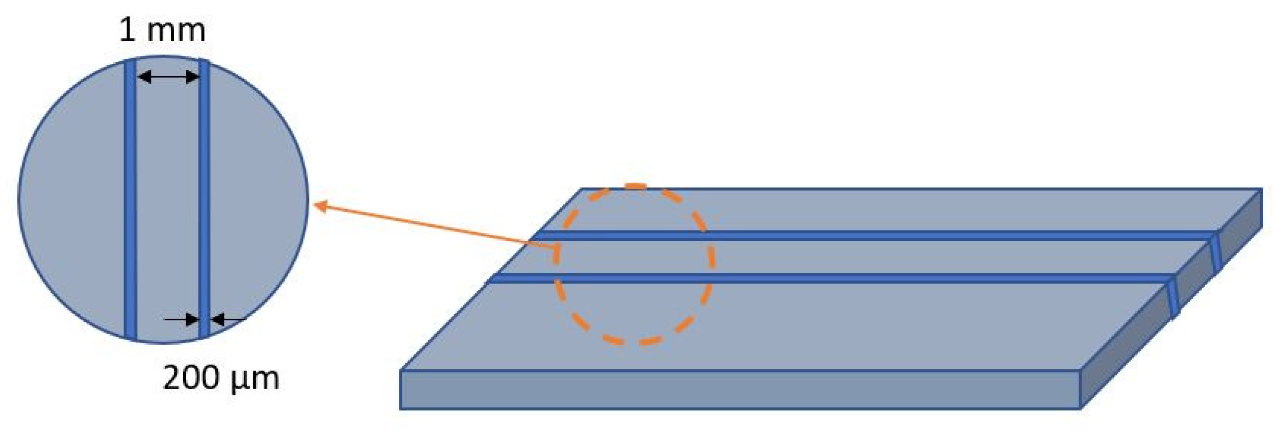
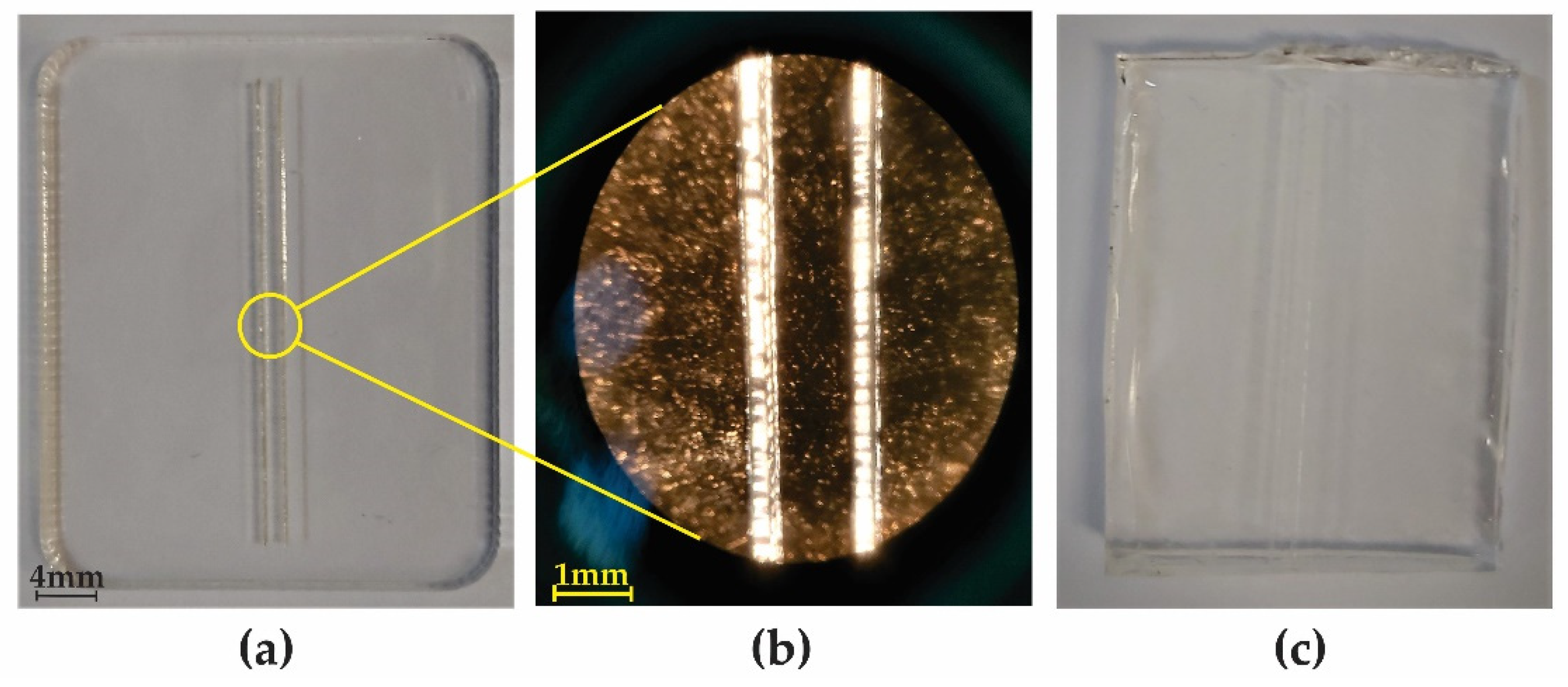
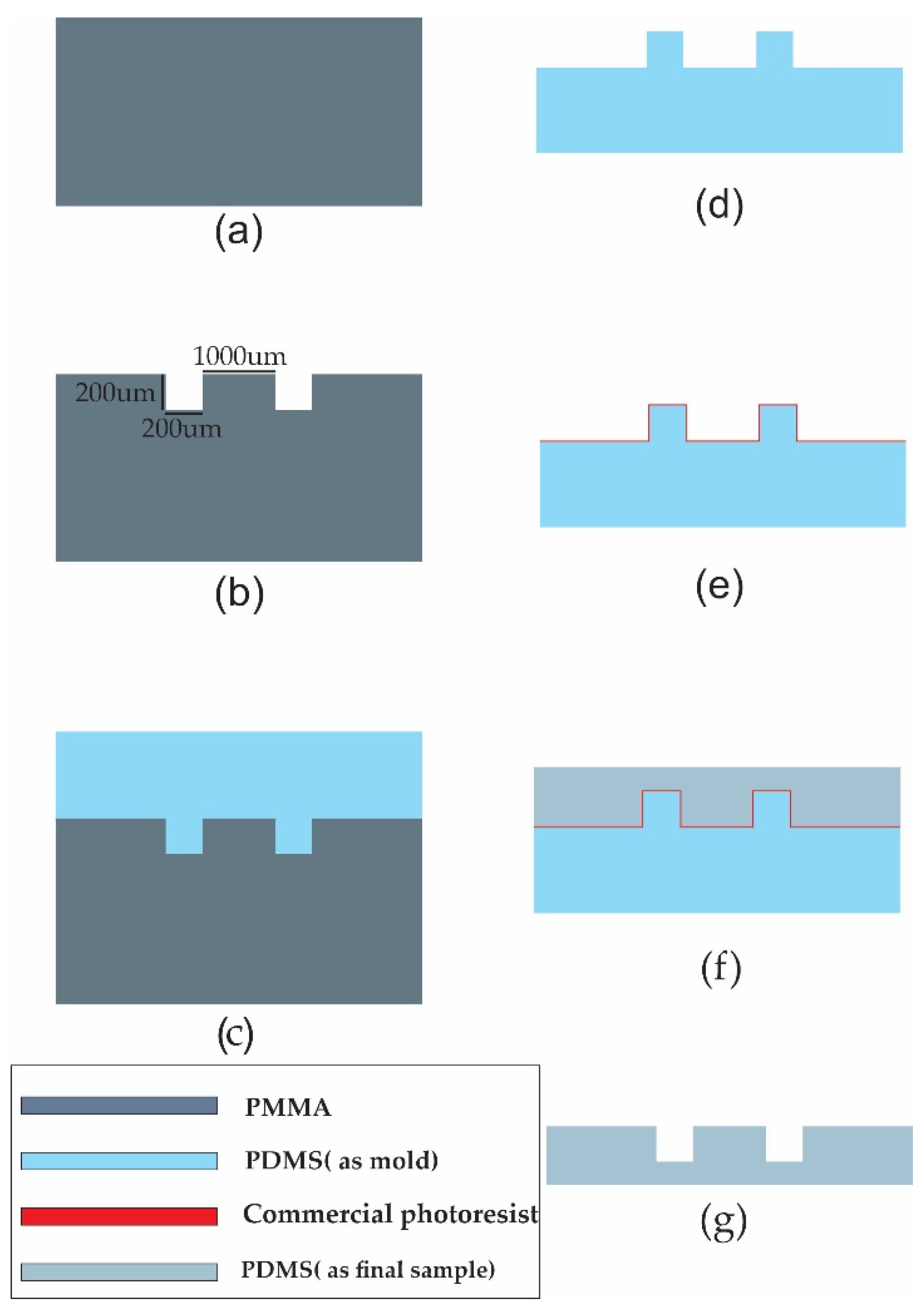
2. Materials and Methods

To fabricate the device firstly, we designed the desired pattern using COREL DRAW. After that, a conventional laser engraver was used to make patterns on the PMMA. PMMA was chosen as scaffold material due to its availability and the fact that high accuracy can be easily achieved with conventional laser. Lasers’ power and delay time were optimized to obtain the best result on the PMMA scaffold. The chosen design contained two parallel lines with a thickness of 200 micrometers and a distance of 1000 micrometers from each other, as shown in Figure 1.
After that, for mold fabrication, RTV-2 was chosen for the first test. Its mixture was made by adding the second part of RTV-2 and diluent liquid, 4% and 5% of the mass, respectively, and then adequately mixed with a glass stirring rod. Then the mixture was placed in a desiccator to eliminate the bubbles for less than 5 min. After that, it was poured on the scaffold and cured for 24 h on a hotplate at 120 °C. The resulted mold was so sticky and unsuitable for our needs.
Ecoflex00-30 was the second material tested for mold fabrication. Its two parts were homogenized in 1:1 ratio and bubbles were eliminated in the same manner previously described. The resulting compound was poured on the scaffold and allowed to cure for 1 h in an oven at 60 °C. After the curing phase, it was clear that Ecoflex00-30 was stuck to the PMMA scaffold and couldn’t be peeled off properly.
The PDMS substance was the third to be tried. SYLGARD 184 was the product that we utilized. The curing agent and base elastomer were combined in a 1:10 ratio to achieve our desired mechanical characteristics. After that, a desiccator was used for around 20 min to clear all of the bubbles. The mixture was then poured over the scaffold and left to cure for one hour in the oven at 85 °C. The PDMS mold simply separated from the PMMA surface due to the poor adhesion between PMMA and PDMS. Patterns on the PDMS mold were evaluated and found to be in good condition. The final PDMS mold and PMMA scaffold are shown in Figure 2.
Since both the mold and sample were made from PDMS, an anti-adhesion layer was essential to make two layers separation feasible. After selecting the best material for mold fabrication, several anti-adhesion coatings such as silicon spray, water and sugar solvent, and a typical commercial photoresist were investigated. Peeling off was feasible with the applying a silicon spray layer, although patterns were not in the ideal condition, and peeling off thin sample layers was challenging. The water and sugar solvent with different concentrations prevent two layers from adhering, but patterns were not adequate because of the considerable sugar particles size compared to micropatterns. As the last tested anti-adhesion layer, a low-cost commercial photoresist, was spin-coated on the mold and baked at 90 °C for around 10 min. The desired photoresist should only have the appropriate density to achieve a layer with a thickness in the range of micrometers after spin coating. Additionaly, it should be detached from the PDMS surface without any damage to the surface. As a result, it could be any commercial photoresist without any critical consideration. Here, after spin coating, a layer with a thickness of about 2 micrometers was obtained, which was thin enough compared to patterns. Using photoresist, the sample was separated from the mold effortlessly and patterns on the sample were in very good shape.
For the sample layer, PDMS was made as explained before and the mixture was spin-coated on the photoresist. Spin-coating was started at 400 rpm/s and continued in 500 rpm/s to obtain a 300 micrometers thickness uniform layer which was then cured for 1 h at 85 °C in the oven. After curing was completed, two layers were separated pretty readily and patterns were in the best shape. Figure 3 represents the entire procedure and Figure 4 depicts the final sample results. Different tested substrate materials and results are summarized in Table 1.

3. Discussion

In this work, a new fabrication method of micropatterning on PDMS substrate was proposed. The presented fabrication approach doesn’t include the standard photolithography process so it doesn’t necessitate expensive material, equipment, and professionalists making it a simple cost-effective patterning method. Compared to other methods [28,29], we didn’t add any extra materials to PDMS to make it photosensitive in our novel patterning approach, either. This is important since any other additives would change PDMS characteristics, such as biocompatibility and flexibility. When benzophenone is added to PDMS, for example, live cells would inevitably die [31]. The use of photoPDMS (PDMS with photosensitive particles inserted) may hinder bioapplications, necessitating the use of an extraction method. In the extraction step, several different chemical materials such as n-pentane, xylene, ethanol (200 proof) are employed to unbound oligomers and enhance polymer cross-linking [31]. Although the extraction process would promote PDMS biocompatibility, it alters material properties and this might be undesired, thus the new form of PDMS should be characterized like the way it’s done in [32]. Added materials are costly, as well as, this process might take several days to be completed.
The fabrication of 3D-printed-based molds can be done in two ways. The traditional technique of 3D printing employs unsolved materials, demanding a peeling-off procedure. Due to the unavoidable peeling off step, micropatterns on micro thickness substrates can not be achievable. In comparison with the solvable 3D-printing-based technique, our method has the advantage of being reusable. If 3D-printed solvable molds are employed to achieve micropatterns, the built mold can only be used once. As a result, the entire patterning process takes a lot more time and money. However, PDMS-based molds are used in this paper, making the procedure repeatable. Table 2 shows a summary of techniques to produce micropatterns on PDMS.

4. Conclusions

In this article, we proposed an innovative and cost-effective method for creating micropatterns on PDMS substrate. There was a biocompatible, micrometer thickness, and the sample substrate desired, leading to the choice of PDMS as the material for the sample substrate. We optimized a conventional laser engraver to create our desired pre-designed pattern on a PMMA sheet, then used it as the scaffold. Following that, Ecoflex 00-30, RTV-2, and PDMS were evaluated to determine the best mold material candidate. PDMS was found to be the best option, benefiting its flexibility property making it possible to be peeled off from scaffold without causing any damage. Choosing PDMS for both mold and sample material required an anti-adhesion layer to make mold and sample separation feasible. Silicon spray, water and sugar mixture in different concentrations, and a low-cost photoresist were tested to hinder mold and sample adhesion. The low-cost photoresist was the final choice because of its desired density and thickness, and also it could be spin-coated on mold leading to a uniform layer. Using this photoresist, the sample was separated from the mold easily and patterns were in good shape indicating that microfeature-size patterns on micro thickness substrate layers are achievable employing the presented method.

Author Contributions

Conceptualization, F.M. and F.S.; methodology, F.M. and F.S.; investigation, F.M.; resources, M.F.; data curation, F.M. and F.S.; writing—original draft preparation, F.M.; writing—review and editing, F.S.; visualization, F.M. and F.S.; supervision, F.S. and M.F.; project administration, F.S. All authors have read and agreed to the published version of the manuscript.

Funding

This research received no external funding.

Institutional Review Board Statement

Not applicable.

Informed Consent Statement

Not applicable.

Conflicts of Interest

The authors declare no conflict of interest.

References

  1. Heath, J.R.; Ratner, M.A. Molecular Electronics; American Institute of Physics: College Park, MD, USA, 2003. [Google Scholar]
  2. Li, L.; Chin, W.S. Rapid fabrication of a flexible and transparent Ag Nanocubes@ PDMS Film as a SERS substrate with high performance. ACS Appl. Mater. Interfaces 2020, 12, 37538–37548. [Google Scholar] [CrossRef] [PubMed]
  3. Qi, D.; Zhang, K.; Tian, G.; Jiang, B.; Huang, Y. Stretchable electronics based on PDMS substrates. Adv. Mater. 2021, 33, 2003155. [Google Scholar] [CrossRef] [PubMed]
  4. Yu, Y.; Peng, S.; Blanloeuil, P.; Wu, S.; Wang, C.H. Wearable Temperature Sensors with Enhanced Sensitivity by Engineering Microcrack Morphology in PEDOT: PSS–PDMS Sensors. ACS Appl. Mater. Interfaces 2020, 12, 36578–36588. [Google Scholar] [CrossRef] [PubMed]
  5. Chen, J.; Zhu, Y.; Jiang, W. A stretchable and transparent strain sensor based on sandwich-like PDMS/CNTs/PDMS composite containing an ultrathin conductive CNT layer. Compos. Sci. Technol. 2020, 186, 107938. [Google Scholar] [CrossRef]
  6. Ko, H.C.; Stoykovich, M.P.; Song, J.; Malyarchuk, V.; Choi, W.M.; Yu, C.J.; Geddes Iii, J.B.; Xiao, J.; Wang, S.; Huang, Y.; et al. A hemispherical electronic eye camera based on compressible silicon optoelectronics. Nature 2008, 454, 748–753. [Google Scholar] [CrossRef] [PubMed]
  7. Seo, H.W.; Kim, N.; Kim, S. Fabrication of subretinal 3D microelectrodes with hexagonal arrangement. Micromachines 2020, 11, 467. [Google Scholar] [CrossRef]
  8. Zhou, M.; Kang, D.H.; Kim, J.; Weiland, J.D. Shape morphable hydrogel/elastomer bilayer for implanted retinal electronics. Micromachines 2020, 11, 392. [Google Scholar] [CrossRef] [Green Version]
  9. Choi, M.C.; Kim, Y.; Ha, C.S. Polymers for flexible displays: From material selection to device applications. Prog. Polym. Sci. 2008, 33, 581–630. [Google Scholar] [CrossRef]
  10. Ojuroye, O.; Torah, R.; Beeby, S. Modified PDMS packaging of sensory e-textile circuit microsystems for improved robustness with washing. Microsyst. Technol. 2019, 1–18. [Google Scholar] [CrossRef] [Green Version]
  11. Choi, S.; Han, S.I.; Kim, D.; Hyeon, T.; Kim, D.H. High-performance stretchable conductive nanocomposites: Materials, processes, and device applications. Chem. Soc. Rev. 2019, 48, 1566–1595. [Google Scholar] [CrossRef]
  12. Kim, J.; Lee, M.; Shim, H.J.; Ghaffari, R.; Cho, H.R.; Son, D.; Jung, Y.H.; Soh, M.; Choi, C.; Jung, S.; et al. Stretchable silicon nanoribbon electronics for skin prosthesis. Nat. Commun. 2014, 5, 5747. [Google Scholar] [CrossRef] [PubMed] [Green Version]
  13. Shanehsazzadeh, F.; Rouhi, S.; Ahmadvand, T.; Namazi, M.; Kiani, S.; Fardmanesh, M. A Novel, Low Cost and Versatile Fabrication Method of Flexible Multi-electrode Array for Spinal Cord Stimulation. In Proceedings of the 2020 27th National and 5th International Iranian Conference on Biomedical Engineering (ICBME), Tehran, Iran, 26–27 November 2020; pp. 138–142. [Google Scholar]
  14. Hasan, M.N.; Radwan, A.N.; Kim, M.; Kucukal, E.; Maji, D.; Pashaei, V.; Chung, C.Y.; Kakkar, A.; Gurkan, U.A. Emerging micro and nanotechnologies in neuroscience: Devices, fabrication methods, and implementation in monitoring of neural activity and drug delivery. Technology 2019, 7, 57–83. [Google Scholar] [CrossRef]
  15. Ahmadvand, T.; Mirsadeghi, S.; Shanehsazzadeh, F.; Kiani, S.; Fardmanesh, M. A Novel Low-Cost Method for Fabrication of 2D Multi-Electrode Array (MEA) to Evaluate Functionality of Neuronal Cells. Proceedings 2020, 60, 51. [Google Scholar]
  16. Ortigoza-Diaz, J.; Scholten, K.; Larson, C.; Cobo, A.; Hudson, T.; Yoo, J.; Baldwin, A.; Weltman Hirschberg, A.; Meng, E. Techniques and considerations in the microfabrication of Parylene C microelectromechanical systems. Micromachines 2018, 9, 422. [Google Scholar] [CrossRef] [PubMed] [Green Version]
  17. Sanzari, I.; Callisti, M.; De Grazia, A.; Evans, D.J.; Polcar, T.; Prodromakis, T. Parylene C topographic micropattern as a template for patterning PDMS and Polyacrylamide hydrogel. Sci. Rep. 2017, 7, 5764. [Google Scholar] [CrossRef] [PubMed] [Green Version]
  18. Kim, Y.S.; Mahmood, M.; Lee, Y.; Kim, N.K.; Kwon, S.; Herbert, R.; Kim, D.; Cho, H.C.; Yeo, W.H. All-in-One, wireless, stretchable hybrid electronics for smart, connected, and ambulatory physiological monitoring. Adv. Sci. 2019, 6, 1900939. [Google Scholar] [CrossRef] [PubMed] [Green Version]
  19. RTV-2 Silicones; The Durability, Stability and High Temperature Resistance of RTV-2 Silicone Rubber. Available online: https://www.elkem.com/silicones/technologies/elastomers/rtv-2/ (accessed on 28 February 2022).
  20. Armani, D.; Liu, C.; Aluru, N. Re-configurable fluid circuits by PDMS elastomer micromachining. In Proceedings of the Technical Digest. IEEE International MEMS 99 Conference. Twelfth IEEE International Conference on Micro Electro Mechanical Systems (Cat. No. 99CH36291), Orlando, FL, USA, 21 January 1999. [Google Scholar]
  21. Suzuki, Y. Micromachined high-aspect-ratio parylene beam and its application to low-frequency seismometer Micro Electro Mechanical Systems. In Proceedings of the Sixteenth Annual International Conference on Micro Electro Mechanical Systems, MEMS-03 Kyoto, Kyoto, Japan, 23 January 2003. [Google Scholar]
  22. Rousche, P.J.; Pellinen, D.S.; Pivin, D.P.; Williams, J.C.; Vetter, R.J.; Kipke, D.R. Flexible polyimide-based intracortical electrode arrays with bioactive capability. IEEE Trans. Biomed. Eng. 2001, 48, 361–371. [Google Scholar] [CrossRef] [PubMed]
  23. Terkan, K.; Zurita, F.; Jamal Khalaf, T.; Rinklin, P.; Teshima, T.; Kohl, T.; Wolfrum, B. Soft peripheral nerve interface made from carbon nanotubes embedded in silicone. APL Mater. 2020, 8, 101111. [Google Scholar] [CrossRef]
  24. Guo, L.; DeWeerth, S.P. Implementation of integratable PDMS-based conformable microelectrode arrays using a multilayer wiring interconnect technology. In Proceedings of the Annual International Conference of the IEEE Engineering in Medicine and Biology Society, Minneapolis, MN, USA, 3–6 September 2009. [Google Scholar]
  25. Branner, A.; Stein, R.B.; Normann, R.A. Selective stimulation of cat sciatic nerve using an array of varying-length microelectrodes. J. Neurophysiol. 2001, 85, 1585–1594. [Google Scholar] [CrossRef] [Green Version]
  26. McDonnall, D.; Clark, G.A.; Normann, R.A. Interleaved, multisite electrical stimulation of cat sciatic nerve produces fatigue-resistant, ripple-free motor responses. IEEE Trans. Neural Syst. Rehabil. Eng. 2004, 12, 208–215. [Google Scholar] [CrossRef]
  27. Ecoflex TM 00-30. Available online: https://www.smooth-on.com/products/ecoflex-00-30/ (accessed on 28 February 2022).
  28. Cho, D.; Park, J.; Kim, T.; Jeon, S. Recent advances in lithographic fabrication of micro-/nanostructured polydimethylsiloxanes and their soft electronic applications. J. Semicond. 2019, 40, 111605. [Google Scholar] [CrossRef]
  29. Cong, H.; Pan, T. Photopatternable conductive PDMS materials for microfabrication. Adv. Funct. Mater. 2008, 18, 1912–1921. [Google Scholar] [CrossRef]
  30. Chen, Q.; Zhao, J.; Ren, J.; Rong, L.; Cao, P.F.; Advincula, R.C. 3D printed multifunctional, hyperelastic silicone rubber foam. Adv. Funct. Mater. 2019, 29, 1900469. [Google Scholar] [CrossRef]
  31. Millet, L.J.; Jain, A.; Gillette, M.U. Less is More: Oligomer extraction and hydrothermal annealing increase PDMS bonding forces for new microfluidics assembly and for biological studies. bioRxiv 2017, 150953. [Google Scholar] [CrossRef]
  32. Lee, J.N.; Park, C.; Whitesides, G.M. Solvent compatibility of poly (dimethylsiloxane)-based microfluidic devices. Anal. Chem. 2003, 75, 6544–6554. [Google Scholar] [CrossRef] [PubMed]
Figure 1. Schematic of PMMA scaffold design.
Engproc 11 00036 g001
Figure 2. (a) Engraved PMMA based layer to be used as the scaffold; (b) Magnification of engraved patterns on PMMA scaffold; (c) Fabricated mold from PDMS.
Engproc 11 00036 g002
Figure 3. Fabrication procedure. (a) PMMA plate; (b) Engraved PMMA based scaffold; (c) Spin coated PDMS on the scaffold to fabricate mold; (d) Fabricated PDMS based mold; (e) Spin coated anti-adhesion layer on the mold; (f) Spin coated PDMS on the anti-adhesion layer; (g) Final sample after separation from mold and eliminating anti-adhesion layer.
Engproc 11 00036 g003
Figure 4. Final fabricated sample. pattern’s feature size is 200 micrometers.
Engproc 11 00036 g004
Table 1. Different substrate materials and their tested results.
Mold MaterialsPMMA Peeling Off FeasibilitySilicon Spray Anti-Adhesion LayerWater and Sugar Solution Anti-Adhesion LayerCommercial Photoresist Anti-Adhesion Layer
RTV-2
Ecoflex00-30
PDMS
Table 2. Micropattern fabrication techniques on PDMS.
Micropatterning TechniqueAdvantagesFabrication Challenges
photolithography methods
  • Tunable and nanoscale feature size
  • complex fabrication process
  • requiring high-cost photoresist
  • high-cost additional materials
  • needing extraction process in bioapplications
  • requiring characterization process
Molding techniques
  • achievable microfeature size patterns
  • relatively cost-effective
  • not repeatable
  • high-cost materials
  • slow process
PDMS-based-molding technique
  • achievable microfeature size patterns
  • low cost
  • repeatable
  • requiring optimization for spin coating speed
  • limitation on fabrication of 3D structures
Publisher’s Note: MDPI stays neutral with regard to jurisdictional claims in published maps and institutional affiliations.

