
Design of an LDMOS Transistor Based on the 1 µm CMOS Process for High/Low Power Applications †


Abstract
:1. Introduction
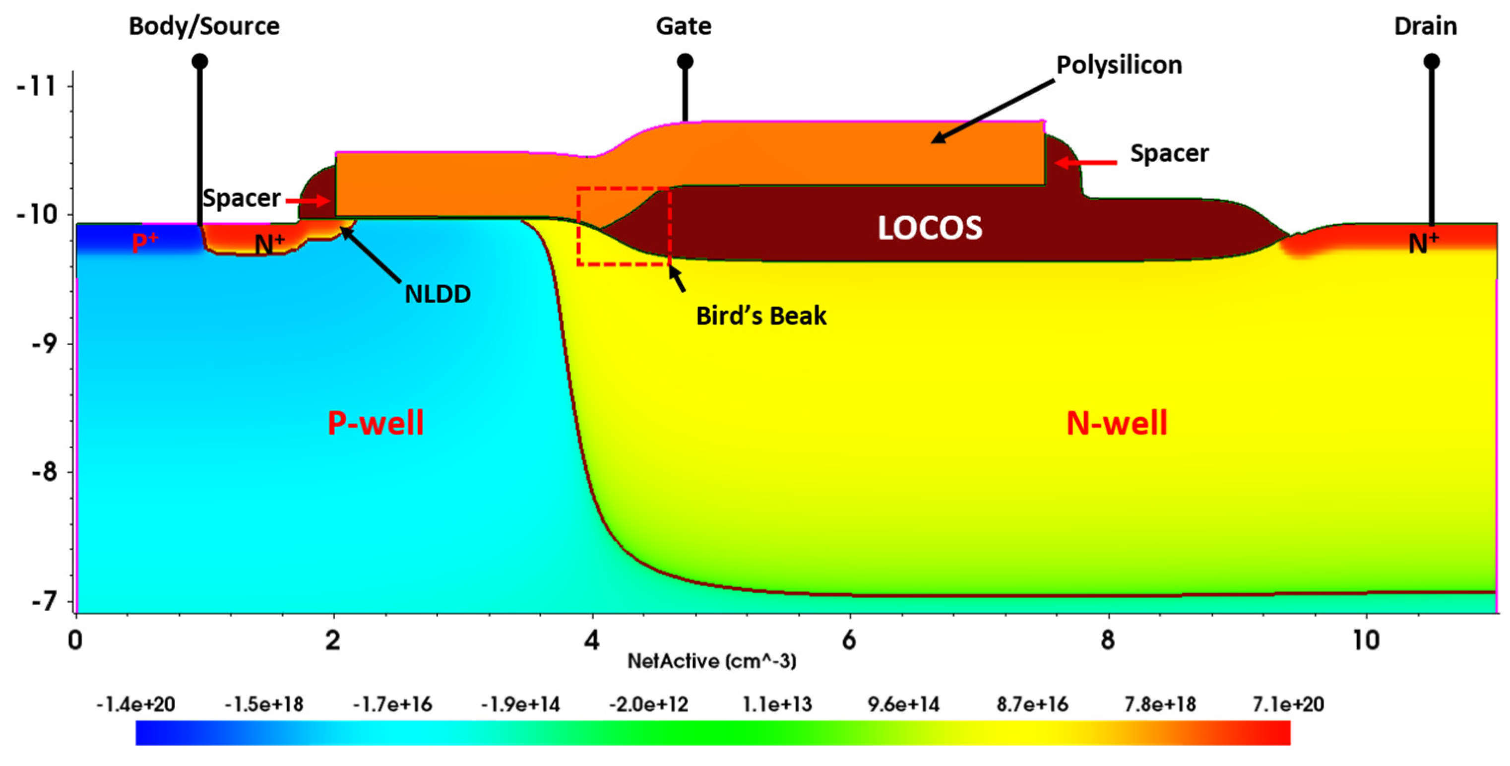
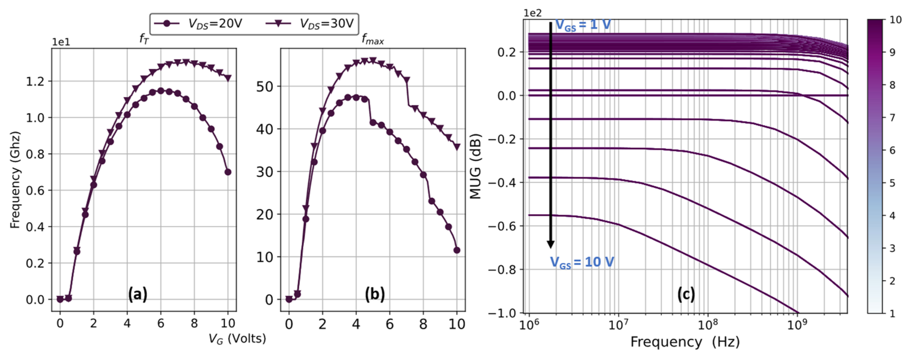
2. Results and Discussion
3. Conclusions
Author Contributions
Funding
Institutional Review Board Statement
Informed Consent Statement
Data Availability Statement
Conflicts of Interest
References
- Ma, G.; Burger, W.; Dragon, C.; Gillenwater, T. High efficiency LDMOS power FET for low voltage wireless communications. In Proceedings of the International Electron Devices Meeting, Technical Digest, San Francisco, CA, USA, 8–11 December 1996; pp. 91–94. [Google Scholar]
- Houadef, A.; Djezzar, B. Process and performance optimization of Triple-RESURF LDMOS with Trenched-Gate. Int. J. RF Microw. Comput.-Aided Eng. 2021, 31, e22755. [Google Scholar] [CrossRef]
- Golio, M. RF and Microwave Semiconductor Device Handbook; CRC Press: Boca Raton, FL, USA, 2017. [Google Scholar]
- Kwon, O.K.; Ng, W.T. Others An optimized RESURF LDMOS power device module compatible with advanced logic processes. In Proceedings of the 1992 International Technical Digest on Electron Devices Meeting, San Francisco, CA, USA, 13–16 December 1992; pp. 237–240. [Google Scholar]
- Tan, Y.; Kumar, M.; Sin, J.K.; Cai, J.; Lau, J. A LDMOS technology compatible with CMOS and passive components for integrated RF power amplifiers. IEEE Electron Device Lett. 2000, 21, 82–84. [Google Scholar] [CrossRef]
- Fu, Y.; Li, Z.; Ng, W.T.; Sin, J.K. Integrated Power Devices and TCAD Simulation; CRC Press: Boca Raton, FL, USA, 2014. [Google Scholar]
- Houadef, A.; Djezzar, B. Hot Carrier Degradation in Triple-RESURF LDMOS with Trenched-Gate. In Proceedings of the 2021 IEEE 32nd International Conference on Microelectronics (MIEL), Nis, Serbia, 12–14 September 2021; pp. 141–144. [Google Scholar]
- Djezzar, B.; Bellaroussi, M.T. Process and Device Simulation of 1.2 μm- Channel N- well C-MOS Technology. In Proceedings of the 5th International Conference on Microelectronics (ICM’93), Dhahran, Saudi Arabia, 14–16 December 1993; pp. 28–32. [Google Scholar]
- Boubaaya, M.; Larbi, F.H.H.; Oussalah, S. Simulation of Ion Implantation for CMOS 1 μm Using SILVACO Tools. In Proceedings of the 2012 24th International Conference on Microelectronics (ICM), Algiers, Algeria, 16–20 December 2012. [Google Scholar]
- Whiston, S.; Bain, D.; Deignan, A.; Pollard, J.; Chleirigh, C.N.; O’Neill, C.M.M. Complementary LDMOS transistors for a CMOS/BiCMOS process. In Proceedings of the 12th International Symposium on Power Semiconductor Devices and ICs. Proceedings (Cat. No. 00CH37094), Toulouse, France, 22–25 May 2000; pp. 51–54. [Google Scholar]
- Ma, G.; Burger, W.; Shields, M. High efficiency 0.4/spl mu/m gate LDMOS power FET for low voltage wireless communications. In Proceedings of the 1999 IEEE MTT-S International Microwave Symposium Digest (Cat. No. 99CH36282), Anaheim, CA, USA, 13–19 June 1999; Volume 3, pp. 1195–1198. [Google Scholar]
- Gray, P.R.; Meyer, R.G. Future directions in silicon ICs for RF personal communications. In Proceedings of the Proceedings of the IEEE 1995 Custom Integrated Circuits Conference, Santa Clara, CA, USA, 1–4 May 1995; pp. 83–90. [Google Scholar]
- SentaurusTM Process User Guide 2017; Synopsys: Mountain View, CA, USA, 2017.
- SentaurusTM Device User Guide 2017; Synopsys: Mountain View, CA, USA, 2017.
- Hower, P.; Lin, J.; Pendharkar, S.; Hu, B.; Arch, J.; Smith, J.; Efland, T. A rugged LDMOS for LBC5 technology. In Proceedings of the 17th International Symposium on Power Semiconductor Devices and ICs, Santa Barbara, CA, USA, 23–26 May 2005; pp. 327–330. [Google Scholar]
- Najafizadeh, L.; Filanovsky, I.M. A simple voltage reference using transistor with ZTC point and PTAT current source. In Proceedings of the 2004 IEEE International Symposium on Circuits and Systems (IEEE Cat. No. 04CH37512), Vancouver, BC, Canada, 23–26 May 2004; Volume 1, pp. 1–909. [Google Scholar]
- Houadef, A.; Djezzar, B. HCI Degradation of LOCOS-based LDMOS Transistor fabricated by 1 μm CMOS Process. In Proceedings of the 2020 International Conference on Electrical Engineering (ICEE), Istanbul, Turkey, 25–27 September 2020; pp. 1–6. [Google Scholar]
- Houadef, A.; Djezzar, B. Evaluation of Hot Carrier Impact on Lateral-DMOS with LOCOS feature. Alger. J. Signals Syst. 2021, 6, 16–23. [Google Scholar]


| Parameter | Value |
|---|---|
| Off-state current (Ioff) @VDS = 30 V | 1.7 × 10⁻¹¹ (A) |
| ON-state current (ION) @ VDS = 30 V | 0.126 (A) |
| Threshold voltage (VTH) @ VDS = 30 V | 0.44 (V) |
| Peak transconductance | 0.136 (S) |
| Zero-temperature coefficient (ZTC) | 1.6 (V) |
| Subthreshold swing (SS) | 105 mV/dec |
| On-state resistance (RON) | 272 (mm2 mΩ) |
| Breakdown voltage (BV) | 22 (V) |
| Figure of merit (FoM) (FoM = BV2/RON) | 1.77 (V/mm2 mΩ) |
| Maximum oscillation frequency (fmax)-PeakdB- | 56.07 (GHz) |
| Cut-off frequency (fT)-Peak0- | 13.14 (GHz) |
Publisher’s Note: MDPI stays neutral with regard to jurisdictional claims in published maps and institutional affiliations. |
© 2022 by the authors. Licensee MDPI, Basel, Switzerland. This article is an open access article distributed under the terms and conditions of the Creative Commons Attribution (CC BY) license (https://creativecommons.org/licenses/by/4.0/).
Share and Cite
Houadef, A.; Djezzar, B. Design of an LDMOS Transistor Based on the 1 µm CMOS Process for High/Low Power Applications. Eng. Proc. 2022, 14, 17. https://doi.org/10.3390/engproc2022014017
Houadef A, Djezzar B. Design of an LDMOS Transistor Based on the 1 µm CMOS Process for High/Low Power Applications. Engineering Proceedings. 2022; 14(1):17. https://doi.org/10.3390/engproc2022014017
Chicago/Turabian StyleHouadef, Ali, and Boualem Djezzar. 2022. "Design of an LDMOS Transistor Based on the 1 µm CMOS Process for High/Low Power Applications" Engineering Proceedings 14, no. 1: 17. https://doi.org/10.3390/engproc2022014017
APA StyleHouadef, A., & Djezzar, B. (2022). Design of an LDMOS Transistor Based on the 1 µm CMOS Process for High/Low Power Applications. Engineering Proceedings, 14(1), 17. https://doi.org/10.3390/engproc2022014017