A Tunable CMOS Image Sensor with High Fill-Factor for High Dynamic Range Applications †

Abstract
:1. Introduction
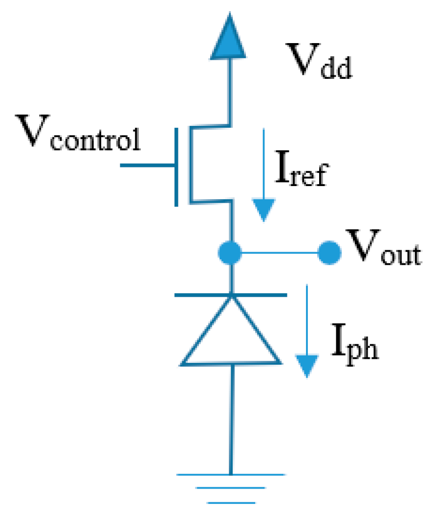
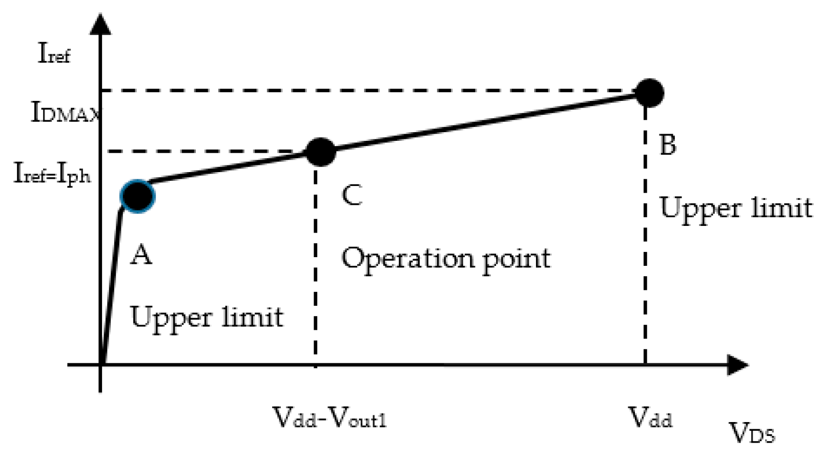
2. Operation Mode
3. Material and Methods
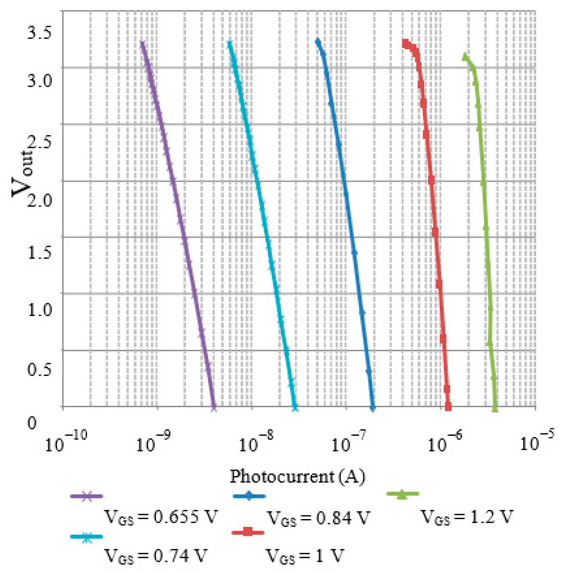
4. Results and Discussion
5. Conclusions
References
- Belenky, A.; Fish, A.; Spivak, A.; Yadid-Pecht, O. A snapshot CMOS image sensor with extended dynamic range. IEEE Sens. J. 2009, 9, 103–111. [Google Scholar] [CrossRef]
- Campos, F.S.; Marinov, O.; Faramarzpour, N.; Saffih, F.; Deen, M.J.; Swart, J.W. A multisampling time-domain CMOS imager with synchronous readout circuit. Analog Int. Circuits Signal Proc. 2008, 57, 151–159. [Google Scholar] [CrossRef]
- Park, D.; Rhee, J.; Joo, Y. A wide dynamic-range CMOS image sensor using self-reset technique. IEEE Dev. Lett. 2007, 28, 890–892. [Google Scholar] [CrossRef]
- McIlrath, L.G. A low-power low-noise ultrawide-dynamic range CMOS imager with pixel-parallel A/D conversion. IEEE J. Solid-State Circuits 2001, 36, 846–853. [Google Scholar] [CrossRef]
- Yang, D.; El Gamal, A.; Fowler, B.; Tian, H. A 640 × 512 CMOS image sensor with ultra wide dynamic range floating point pixel level ADC. IEEE J. Solid-State Circuits 1999, 34, 1821–1834. [Google Scholar] [CrossRef]
- Decker, S.; McGrath, R.D.; Brehmer, K.; Sodini, G. A 256 × 256 CMOS imaging array with wide dynamic range pixels and column parallel digital output. IEEE J. Solid-State Circuits 1998, 33, 2081–2091. [Google Scholar] [CrossRef]
- Seo, M.-W.; Sawamoto, T.; Akahori, T.; Liu, Z.; Iida, T.; Takasawa, T.; Kosugi, T.; Watanabe, T.; Isobe, K.; Kawahito, S. A low-noise high-dynamic-range 17b 1.3-Megapixel 30-fps CMOS image sensor with column-parallel two-stage folding-integration/cyclic ADC. IEEE Trans. Electron. Devices 2012, 59, 3396–3400. [Google Scholar] [CrossRef]
- Ignjatovic, Z.; Maricic, D.; Bocko, M.F. Low power, high dynamic range CMOS image sensor employing pixel-level oversampling ΣΔ analog-to-digital conversion. IEEE Sens. J. 2012, 12, 737–746. [Google Scholar] [CrossRef]
- Seo, M.W.; Suh, S.-H.; Iida, T.; Takasawa, T.; Isobe, K.; Watanabe, T.; Itoh, S.; Yasutomi, K.; Kawahito, S. A low-noise high intrascene dynamic range CMOS image sensor with a 13 to 19b variable-resolution column-parallel folding-integration/cyclic ADC. IEEE J. Solid-State Circuits 2012, 47, 272–283. [Google Scholar] [CrossRef]
- Chae, Y.C.; Cheon, J.M.; Lim, S.H.; Kwon, M.H.; Yoo, K.S.; Jung, W.K.; Lee, D.H.; Ham, S.H.; Han, G.H. A 2.1 M pixels, 120frames/s CMOS image sensor with column-parallel ΔΣ ADC architecture. IEEE J. Solid-State Circuits 2011, 46, 236–247. [Google Scholar] [CrossRef]
- Park, J.H.; Ayoama, S.; Watanabe, T.; Isobe, K.; Kawahito, S. A high-speed low noise CMOS image sensor with 13-b column-parallel single-ended cyclic ADCs. IEEE Trans. Electron. Devices 2009, 56, 2414–2422. [Google Scholar] [CrossRef]
- Furuta, M.; Nishikawa, Y.; Kawahito, S. A high-speed, high-sensitivity digital CMOS image sensor with a global shutter and 12-bit column-parallel cyclic A/D converter. IEEE J. Solid-State Circuits 2007, 42, 766–774. [Google Scholar] [CrossRef]
- El-Desouki, M.M.; Palubiak, D.; Deen, M.J.; Fang, Q.; Marinov, O. A Novel, High Dynamic Range, High Speed and High Sensitivity CMOS Imager Using Time-Domain Single Photon Counting and Avalanche Photodiodes. IEEE Sens. J. 2011, 11, 1078–1083. [Google Scholar] [CrossRef]
- Campos, F.S.; Faramarzpour, N.; Marinov, O.; Deen, M.J.; Swart, J.W. Photodetection with Gate-Controlled Lateral BJTs from Standard CMOS Technology. IEEE Sens. J. 2013, 13, 1554–1563. [Google Scholar] [CrossRef]
- Faramarzpour, N.; El-Desouki, M.M.; Deen, M.J.; Shirani, S.; Fang, Q. CMOS Photodetector Systems for Low-Level Light Applications. J. Mater. Sci. Mater. Electron. 2009, 20, S87–S93. [Google Scholar] [CrossRef]
Publisher’s Note: MDPI stays neutral with regard to jurisdictional claims in published maps and institutional affiliations. |
© 2020 by the authors. Licensee MDPI, Basel, Switzerland. This article is an open access article distributed under the terms and conditions of the Creative Commons Attribution (CC BY) license (https://creativecommons.org/licenses/by/4.0/).
Share and Cite
Campos, F.d.S.; Castro, B.A.d.; Swart, J.W. A Tunable CMOS Image Sensor with High Fill-Factor for High Dynamic Range Applications. Eng. Proc. 2020, 2, 79. https://doi.org/10.3390/ecsa-7-08235
Campos FdS, Castro BAd, Swart JW. A Tunable CMOS Image Sensor with High Fill-Factor for High Dynamic Range Applications. Engineering Proceedings. 2020; 2(1):79. https://doi.org/10.3390/ecsa-7-08235
Chicago/Turabian StyleCampos, Fernando de Souza, Bruno Albuquerque de Castro, and Jacobus W. Swart. 2020. "A Tunable CMOS Image Sensor with High Fill-Factor for High Dynamic Range Applications" Engineering Proceedings 2, no. 1: 79. https://doi.org/10.3390/ecsa-7-08235