1. Introduction
The reliability of microsystems might get largely affected by defects or fluctuations in their properties, as induced by the fabrication process [
1,
2,
3,
4]. This is nowadays becoming more and more a crux, due to the downsize of the devices induced by economic reasons. Errors or, with more appropriate words, sensitivity to imperfections and related scattered responses have been largely reported in the literature, see e.g., [
5].
The mentioned issue requires an in-depth study of the uncertainties (uncertainty quantification) to be carried out [
6,
7], in order to pinpoint the major micromechanically-governed parameters that affect the figures of merit of off-the-shelf devices. For instance, within a coupled multi-physics framework, in [
8,
9] the optimization of the geometry of resonant Lorentz force magnetometers was approached; it was observed that, in order to maximize the performances of the devices, the geometry and the actuation features may get close to some unstable solutions, which are even more sensitive to imperfections. In [
10], the imperfections in one of those devices were considered to consist of the fluctuations of the local elasticity in the structural film constituting the movable part of the devices, as induced by its polycrystalline morphology [
11,
12,
13], and of the overetch, which is obviously affected on its own by the so-called etch environment and may not prove to be isotropic and homogeneous within a single die.
To bring the optimization of sensor performances and sensitivity to imperfections into a kind of robust optimization procedure, starting in [
14] we proposed an on-chip testing device characterized by a very slender part of the movable structure, with an in-plane width at the lower bound for the adopted micro-fabrication process. The actual aim of the proposed solution was to enhance as much as possible the mentioned sensitivity of the measurable response to local morphological properties. The mechanical properties of the testing device were investigated in terms of their overall values and also in terms of their intra-die and inter-die variations, giving rise to the observed scattered responses. Various approaches were adopted to carry out this characterization, ranging from particle filtering [
14] to genetic algorithms [
15] and full Monte Carlo analyses [
16], see also [
17]. Even if the major causes of the scattering were highlighted, also via sensitivity analysis, results were never close enough to the experimental data as testified by some unphysical actuation-dependent solutions at constant imperfection patterns.
In this work, we aim to extend and improve the former studies by accounting for some recent results described in [
18], to feed a methodology able to account for local fluctuations of the imperfections in a more accurate and robust way. The improvement consists in subdividing the structural components subjected to the major deformation field into smaller blocks, locally upscaling the elastic properties and then assembling everything to stochastically describe the overall device response.
The remainder of the paper is organized as follows. In
Section 2 we describe the main features of the designed on-chip testing device, and the theoretical model under different actuation types. In
Section 3 we provide details on the way stochastic effects are accounted for, and a comparison is shown between the experimental data and the outcomes of the proposed model. Some conclusions on the activity are carried out, and further developments currently under way are finally mentioned in
Section 4.
2. On-Chip Testing Device
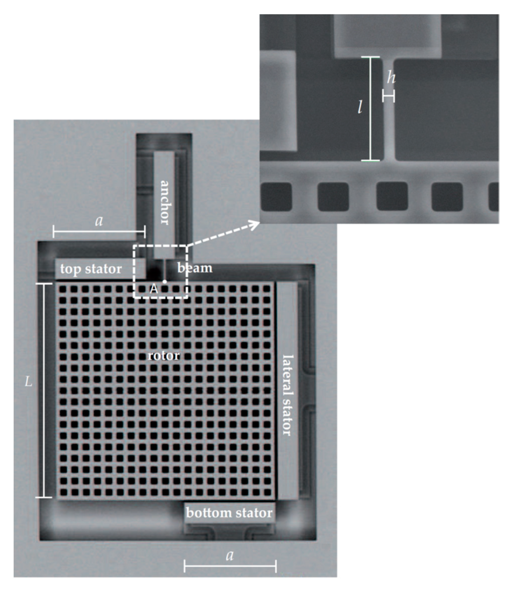
The geometry of the designed on-chip testing device is depicted in
Figure 1; the relevant dimensions are gathered in
Table 1. The movable part of the device, denoted as rotor in the SEM picture, is constituted by a perforated proof mass of side length
, connected to the substrate by means of the slender beam at the top, of length
and width
as highlighted in the close-up. By connecting the rotor to a single anchor, so by adopting a statically determinate structural configuration, the effects of residual stresses induced by the micro-fabrication process have been avoided or reduced to a minimum.
The rotor is surrounded by a couple of top-bottom stators and by a lateral stator, to induce a motion through electrostatic actuation. The top-bottom stators allow inducing a purely flexural deformation of the beam, whereas the lateral stator allows inducing both bending and shear deformations. The two actuation modes have been designed to work side-by-side for each single device, so as to deform/stress in two different ways beams characterized by the same overetch-affected geometry and by the same polycrystalline morphology. In all the devices patterned on a single die, only the length
of the supporting beam has been varied (within a range even larger than the one reported in
Table 1), in order to understand if the film morphology may affect also the kinematics of deformation in case of either slender or short beams. Adopting a Timoshenko beam bending model for the beam [
19], the relation between actuation and deformation reads:
where
and
are the lateral (horizontal in
Figure 1) displacement and (counterclockwise) rotation of the tip A of the beam;
and
are the corresponding horizontal force and counterclockwise bending moment at the same tip A of the beam;
is a non-dimensional factor weighting the effects of bending and shear deformations;
and
are the effective Young’s and shear moduli of the beam (and not of polysilicon, see
Section 3);
and
are the area and moment of inertia of the beam cross-section;
is the shear correction factor, which depends on the shape of the cross-section.
The stators located around the proof mass can induce two modes of deformation in the beam, through two different values of
and
provided by the electrostatic actuation. In the so-called rotational actuation case, when the top and bottom electrodes are used, we have:
where
,
and
being, respectively, the relative permittivity of the medium and the dielectric constant in the free space;
is the initial gap at the electrodes, and all the other dimensions are shown in
Figure 1. In the so-called lateral actuation case, when only the lateral electrode is used, we instead have:
As extensively detailed in [
14,
15], these analytical formulae are obtained moving from the solution for parallel plate capacitors, by assuming that the effects of fringe fields and tilting angle are negligible, and by computing the local variation of the gap at the capacitors as induced by
and
, fully describing the beam deformation. By either setting the actuation voltage
or
, beam deflection can be computed by solving the system of nonlinear Equations (1)–(3).
By exploiting the device configuration above described, two different sensing mechanisms can be also obtained by either measuring the capacitance change at the top-bottom stators or at the lateral stator. The corresponding values of the capacitances are affected by beam deformation according to
In a real experiment, the capacitance change is actually measured either in terms of or of , where and are the values provided by Equation (4) in the unstressed state characterized by , so for an imperfection-free geometry.
By coupling the two actuation modes with the two sensing modes, four different tests can be carried out on each single device to collect some redundant data on its response to the external actions.
3. Stochastic Effects and Scattered Device Response
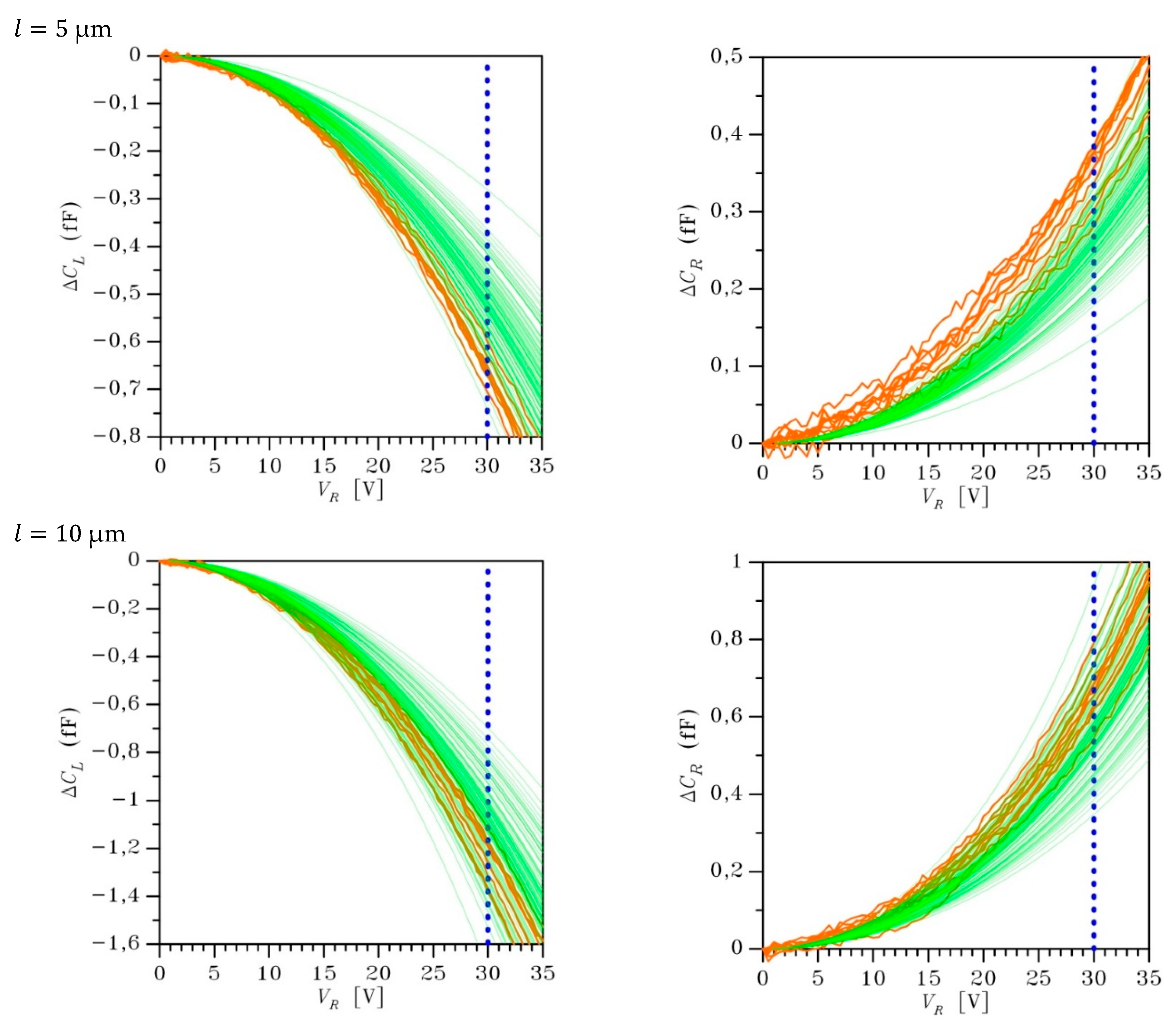
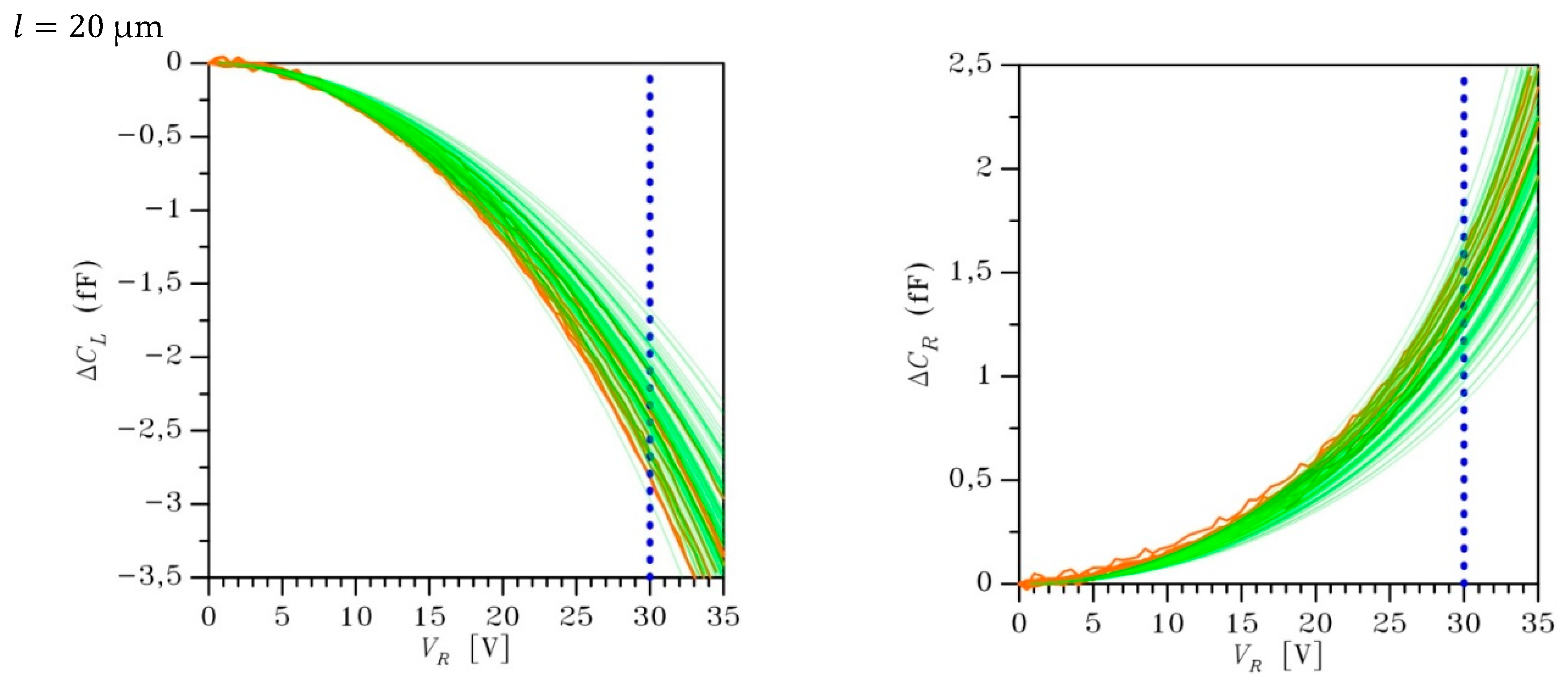
In order to catch the scattering in the experimental data, represented in the charts of
Figure 2 with the orange
(actually
, as discussed in
Section 2) plots, stochastic effects were investigated. A sensitivity analysis allowed to establish that the major source of the reported scattering is related to the elastic stiffness
of the entire supporting beam. On its own, this stiffness is affected by the local fluctuations of the polycrystalline morphology and of the cross-sectional width
. The morphology of the structural film has an impact since each silicon grain is an orthotropic medium, and its contribution to the beam stiffness depends on the orientation of its crystal lattice relative to the longitudinal beam axis. The cross-sectional geometry is instead affected by etch defects, accounted for by the overetch
leading to a heterogeneous beam width. The overetch also affects activation and sensing at the electrodes, since it modifies the initial gap between rotor and stators.
As far as the elasticity of the polysilicon film is concerned, a model was proposed in [
18]. Since the morphology varies along the beam axis in an unpredictable way, a Monte Carlo analysis was resorted to define the effective value of
to be adopted in Equation (1). Statistical volume elements (SVEs), see e.g., [
20], characterizing the actual film morphology, are sampled out of a Voronoi tessellation to feature a side length
mimicking the beam width. A numerical homogenization procedure is adopted to obtain, for each realization in the Monte Carlo analysis, the overall elastic properties. SVEs are then stacked on top of each other till when the specific length
of the beam is attained, as a multiple of the relevant width
. The procedure is repeated a large number of times, in order to finally provide the probability density function (pdf) of
to be adopted in the beam bending model described in Equation (1).
To speed-up the computation of the pdf of
, in [
18] the pdfs for the elastic moduli given by the computational homogenization on the SVEs were fitted with lognormal distributions. In our analysis, we still allow for such pdfs even if they can introduce an approximation in the model. An error then shows up in the results, due to the fact that the width of the beam locally varies and, accordingly, also the side length of the SVEs over which the local stiffness must be evaluated. In accordance with the micro-fabrication specifications, the overetch
can be considered small in comparison to the said beam width, and so the error and the interplay between the statistics of
and
.
Some results of the proposed model are reported in
Figure 2 via the green
plots, and were compared with the experimental data in case of rotational actuation through
only; similar results have been obtained in case of lateral actuation, but are not reported here for brevity. As shown in our previous studies, independently of the beam length the curves are all characterized by negative
values and by positive
values. This is due to the fact that the induced change in the configuration reduces the gaps at the top and bottom stators and increases the gap along the lateral stator, on the average. The maximum reported value for the actuation voltage; that is
V, is rather far from pull-in for
µm but, the other way around, can be even larger than the pull-in one for some compliant configurations featuring
µm, which actually display a vertical asymptote for smaller values of
: in this regard, results show a monotonic trend for increasing values of
. The experimental curves (orange lines) are characterized by fluctuating evolutions of the capacitance changes at increasing
due to the measurement noise, which is indeed clearer for
µm due to the values of
and
close to the capacitance-meter resolution; the model outcomes are instead smooth as they are considered free from measurement noise, which can be anyway added to them to mimic what happens during real testing.
The agreement between the experimental data and the numerical results looks rather good, much better than that achieved in the past by neglecting the variability of
and
along the beam axis, see [
14,
15,
16,
17]. The numerical curves cover in an appropriate way the experimental ones. A slight discrepancy in terms of mean values of
and
for an assigned
is reported only for
µm, the numerical behavior being stiffer than the real ones and therefore characterized by a larger value of the pull-in voltage. This is actually expected, since the slenderness
is rather far from the values within the range of applicability of beam bending theories; they are anyway kept here to show how the model can catch relatively well also the effect of beam slenderness on the device response.
4. Conclusions
In this work, we have discussed a semi-analytical statistical model to describe the scattering in the nonlinear response of an on-chip MEMS testing device, designed to quantify the relevant uncertainties linked to the polysilicon microstructure.
According to former results, the elastic and geometric properties of the supporting beam of the MEMS movable structure have been selected as the main features to induce the measured scattering. Through a beam bending-based model of the entire movable structure, plots have been built for different actuation/sensing modes designed to gather redundant data (prior to pull-in) for each single microstructure. Film grain morphology and etch defects have been then concretely considered as the input parameters in a Monte Carlo analysis to quantify the scattering. In comparison with the mentioned former results, outcomes of the proposed model have been shown to better agree with the experimental data.
Currently, the proposed strategy is going to be re-formulated within the frame of a data-driven approach. Specifically, the mechanical properties of polysilicon are characterized by a neural network, trained with the same data used in this work for upscaling its elastic properties [
21,
22,
23,
24]. Next step of the procedure is therefore the multiscale [
25,
26], fully data-driven analysis of the designed device and, to a larger extent, of the scattering measured in ever downsizing MEMS devices.

 and
and 


