
Effect of Strain on Properties of Metal Doped VO2 Based Thermal Sensors on Muscovite Substrate †


Abstract
:1. Introduction
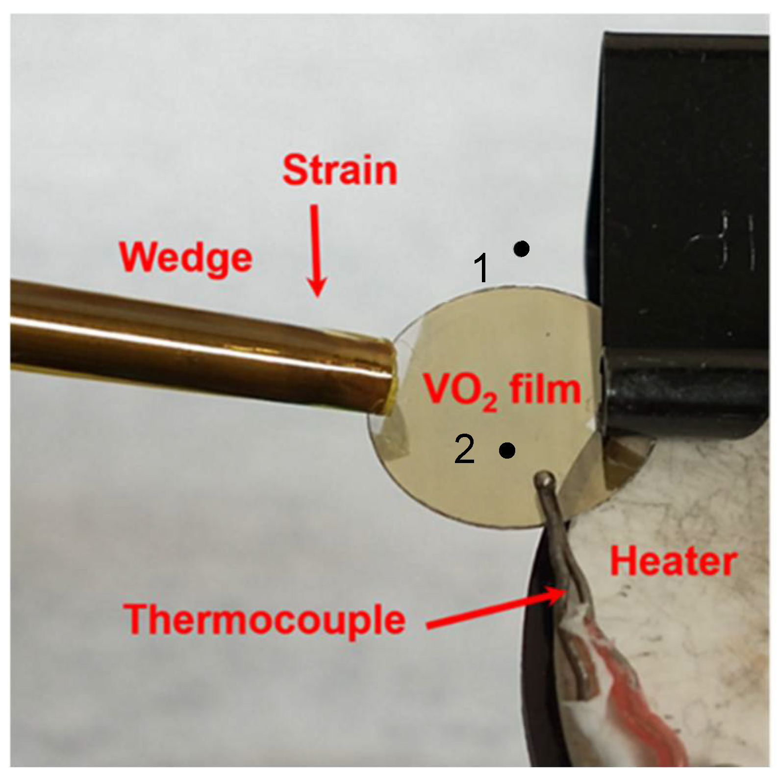
2. Experimental Details
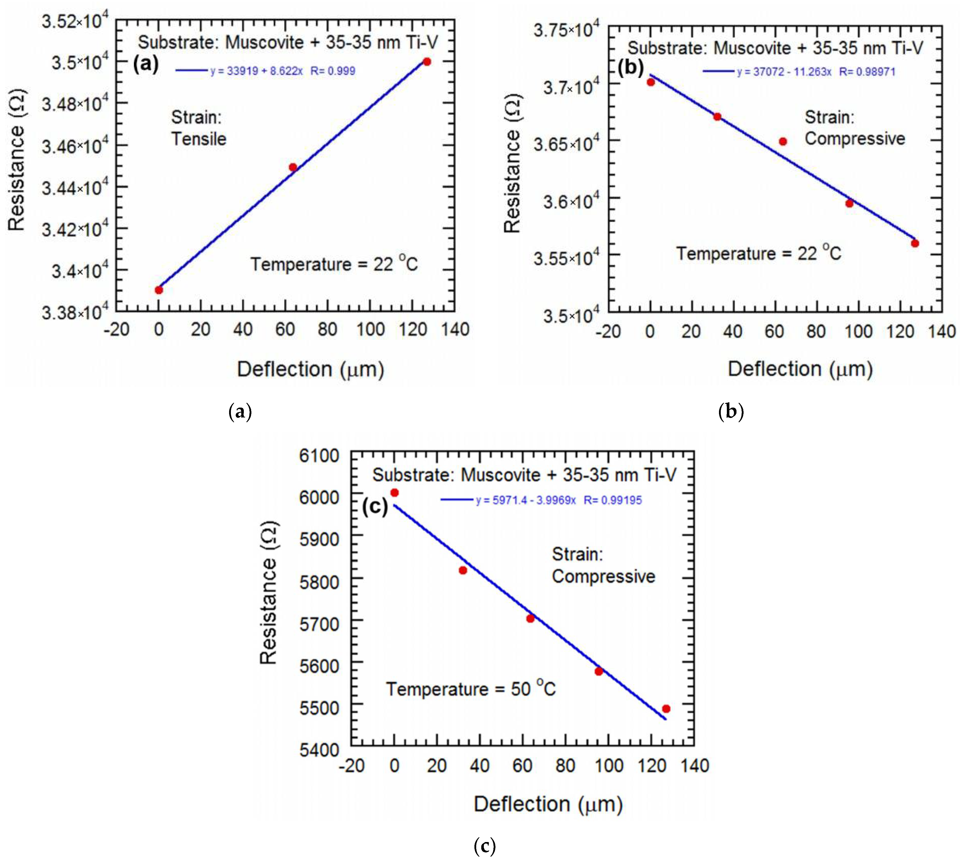
3. Results and Discussion
4. Conclusions
Author Contributions
Funding
Institutional Review Board Statement
Informed Consent Statement
Data Availability Statement
Acknowledgments
Conflicts of Interest
References
- Baqir, M.A.; Choudhury, P.K. On the VO2 metasurface-based temperature sensor. J. Opt. Soc. Am. 2019, 36, F123–F130. [Google Scholar] [CrossRef]
- Cui, Y.; Ke, Y.; Liu, C.; Chen, Z.; Wang, N.; Zhang, L.; Zhou, Y.; Wang, S.; Gao, Y.; Long, Y. Thermochromic VO2 for Energy-Efficient Smart Windows. Joule Cellpress Rev. 2018, 2, 1707–1746. [Google Scholar] [CrossRef] [Green Version]
- Masina, B.N.; Akande, A.A.; Mwakikunga, B. Effect of laser wavelength in PLD in the orientation and thermochromic properties of VO2 (M1) on a glass substrate. MRS Adv. 2020, 5, 1121–1132. [Google Scholar] [CrossRef]
- Lappalainen, J.; Heinilehto, S.; Saukko, S.; Lantto, V.; Jantunen, H. Microstructure dependent switching properties of VO2 thin films. Sens. Actuators 2018, 142, 250–255. [Google Scholar] [CrossRef]
- Zhang, J.; He, H.; Xie, Y.; Pan, B. Giant reduction of the phase transition temperature for beryllium doped VO2. Phys. Chem. Chem. Phys. 2013, 15, 4687–4690. [Google Scholar] [CrossRef] [PubMed]
- Matsuguchi, M.; Uno, T. Molecular imprinting strategy for solvent molecules and its application for QCM-based VOC vapor sensing. Sens. Actuators B 2006, 113, 94–99. [Google Scholar] [CrossRef]
- Azad, S.; Gajula, D.; Koley, G. Infrared Transmission Characteristics of Phase Transitioning VO2 on Various Substrates. Micromachines 2022, 13, 812. [Google Scholar] [CrossRef] [PubMed]
- Azad, S.; Gajula, D.; Koley, G. Synthesis and characterization of VO2 thin films on piezoelectric substrates. Thin Solid Films 2021, 742, 139055. [Google Scholar] [CrossRef]
- Chen, H.-W.; Li, C.-I.; Ma, C.-H.; Chu, Y.-H.; Liu, H.-L. Strain engineering of optical properties in transparent VO2/muscovite heterostructures. Phys. Chem. Chem. Phys. 2021, 23, 8908–8915. [Google Scholar] [CrossRef] [PubMed]
- Kikuzuki, T.; Lippmaa, M. Characterizing a strain-driven phase transition in VO2. Appl. Phys. Lett. 2016, 96, 132207. [Google Scholar] [CrossRef]
- Lee, C. Improving Snapfit Design. 2007. Available online: https://knowledge.ulprospector.com/1248/pe-snapfit-3/ (accessed on 19 February 2007).
- Yu, X.M.; Thaysen, J.; Hansen, O.; Boisen, A. Optimization of sensitivity and noise in piezoresistive cantilevers. J. Appl. Phys. 2002, 92, 6296–6301. [Google Scholar] [CrossRef] [Green Version]
- Qazi, M.; DeRoller, N.; Talukdar, A.; Koley, G. III-V Nitride based piezoresistive microcantilever for sensing applications. Appl. Phys. Lett. 2011, 99, 193508. [Google Scholar] [CrossRef]
- Gajula, D.; Jahangir, I.; Koley, G. High Temperature AlGaN/GaN Membrane Based Pressure Sensors. Micromachines 2018, 9, 207. [Google Scholar] [CrossRef] [PubMed] [Green Version]
- Talukdar, A.; Khan, M.F.; Lee, D.; Kim, S.; Thundat, T.; Koley, G. Piezotransistive transduction of femtoscale displacement for photoacoustic spectroscopy. Nat. Commun. 2015, 6, 7885. [Google Scholar] [CrossRef] [PubMed] [Green Version]
- Talukdar, A.; Koley, G. Impact of Biasing Conditions on Displacement Transduction by III-Nitride Microcantilevers. IEEE Electron Device Lett. 2014, 35, 1299–1301. [Google Scholar] [CrossRef]


Publisher’s Note: MDPI stays neutral with regard to jurisdictional claims in published maps and institutional affiliations. |
© 2022 by the authors. Licensee MDPI, Basel, Switzerland. This article is an open access article distributed under the terms and conditions of the Creative Commons Attribution (CC BY) license (https://creativecommons.org/licenses/by/4.0/).
Share and Cite
Azad, S.; Gajula, D.; Prio, M.H.; Koley, G. Effect of Strain on Properties of Metal Doped VO2 Based Thermal Sensors on Muscovite Substrate. Eng. Proc. 2022, 27, 80. https://doi.org/10.3390/ecsa-9-13320
Azad S, Gajula D, Prio MH, Koley G. Effect of Strain on Properties of Metal Doped VO2 Based Thermal Sensors on Muscovite Substrate. Engineering Proceedings. 2022; 27(1):80. https://doi.org/10.3390/ecsa-9-13320
Chicago/Turabian StyleAzad, Samee, Durga Gajula, Makhluk Hossain Prio, and Goutam Koley. 2022. "Effect of Strain on Properties of Metal Doped VO2 Based Thermal Sensors on Muscovite Substrate" Engineering Proceedings 27, no. 1: 80. https://doi.org/10.3390/ecsa-9-13320
APA StyleAzad, S., Gajula, D., Prio, M. H., & Koley, G. (2022). Effect of Strain on Properties of Metal Doped VO2 Based Thermal Sensors on Muscovite Substrate. Engineering Proceedings, 27(1), 80. https://doi.org/10.3390/ecsa-9-13320