Abstract
Scaling down the form-factor of printed electronics is one of the methods for improving the reliability of printed e-textiles. This also enhances the wearability of the printed e-textile. However, the surface roughness of textiles and the low resolution of current printing methods, such as screen-printing, often present significant challenges for directly realizing microcircuits on textiles that are developed for printed e-textile applications. This work reports the planarization of a polyester cotton textile with a screen-printed polyurethane (PU) smoothing interface layer to enable the micro-patterning of the textile with conductive thin films using microfabrication techniques. Thermally evaporated copper structures with features sized from 800 µm down to 10 µm are patterned on the planar textile, demonstrating a printed resolution that is otherwise difficult to achieve through screen-printing even with the aid of specialized screens.
1. Introduction
The challenge of manufacturing lightweight e-textiles that are unobtrusive and robust against external stresses continues to drive the research and applications of e-textiles. Meeting this need necessitates a reduction in the geometry and size of any integrated electronics on textiles down to the micron scale (<100 µm) [1]. However, the feature resolution of current e-textile manufacturing methods such as printing [2], embroidery [3] and weaving [4] is insufficient to achieve such microcircuits on textiles. Microcircuits for e-textiles are currently manufactured using traditional microfabrication techniques such as photolithography and etching or lift-off processes to create flexible electronic strip circuits suitable for weaving into fabrics [5]. During the weaving manufacturing stresses, this method frequently introduces stresses into the microcircuit. The weaving process further complicates the integration of these strip circuits in fabrics [6].
This study offers preliminary research into an approach that combines low-cost screen-printing with standard microfabrication processes to directly deposit and localize microcircuit patterns on textiles, minimizing integration challenges and benefiting the reliability and wearability of e-textiles. This method also ensures that micropatterns are not strained by the manufacturing process. The proposed e-textile shown in Figure 1 consists of a screen-printed polyurethane (PU) interface layer, which planarizes the textile surface and allows copper micropatterns to be deposited onto it through a combination of photolithography, thermal evaporation deposition and etching processes.
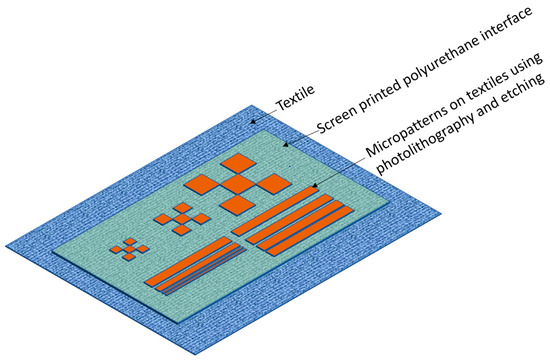
Figure 1.
Proposed e-textile fabricated using screen-printing and microfabrication techniques.
2. Materials and Methods
Polyester cotton fabric supplied by Klopmann Ltd. was chosen as the textile substrate due to its suitability for garment manufacture. Screen-printable UV paste, UV-IF-1004, supplied by Smart Fab inks was used for printing the smoothing polyurethane (PU) interface layer on the fabric because of its good adhesion to printed films [1]. Table 1 lists the solvents used in the lift-off or etching microfabrication processes for patterning the textile.

Table 1.
List of solvents for lift-off and etching processes.
2.1. Screen-Printing and Metallization Processes
Figure 2 shows a 10 cm × 10 cm PU interface layer screen-printed onto the textile using a semi-automatic DEK248 screen-printer with the printing process described in [1]. The average printed PU thickness was 200 µm. The 2D surface topography of the printed textile obtained from a Tencor P11 surface profiler, as shown in Figure 2, clearly indicates a significant reduction in the average surface roughness of the textile from an initial value of 35 µm to 1 µm.
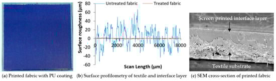
Figure 2.
Morphology and surface topology of printed fabric.
The printed fabric was metallized with 500 nm thick copper film using thermal evaporation deposition. A 10 nm thick chromium film was initially thermally deposited on the PU film to improve the adhesion of the copper film, as shown by the tape test in Figure 3.
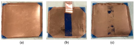
Figure 3.
(a) thermally evaporated copper on interface layer; (b) adhesion of copper without and (c) with chromium layer after tape-test.
2.2. Evaluation of Solvents
To investigate the viability of the lift-off and etch processes in enabling microcircuit patterning on the interface layer, 10 by 85 mm samples of the untreated textile (i.e., without PU) and the PU-coated fabrics were prepared. The samples were immersed in the solvents listed in Table 1 between 5 min and 20 min to determine if the fabrics and PU coating would survive the solvents and their processing times.
2.3. Patterning Proccesses—Photolithography and Etching
To pattern the fabric, a 6 µm-thick negative photoresist, AZ2070, was spin-coated and baked at 110 °C for 3 min before and after UV exposure through a mask containing the different patterns with feature sizes, line width and spacing ranging from 10 µm to 800 µm as shown in Figure 1. The exposed resist was developed for 75 s in AZ726 developer solution, rinsed in de-ionized water and etched for 10 s in ferric chloride (FeCl3) solution. Figure 4 shows the etched sample and the pattern resolutions achieved.
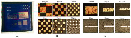
Figure 4.
(a) Etched copper patterns on PU-coated fabrics; (b) feature quality of copper squares of different sizes; (c) resolution of different line width resolution.
3. Results and Discussion
Results comparing the various solvents demonstrate that they attack the PU coating, and this is especially noticeable in the lift-off process. N-Methyl-2-pyrrolidone (NMP), for example, severely degrades the PU coating after 20 min, as shown in Figure 5. The solvents for the etch process had minimal curling effect on the PU coating; hence, it was chosen for this work. For the wet stages of the lift-off and etching methods to be practical for micropatterning e-textiles, polymer friendly and gentle solvents are still required.
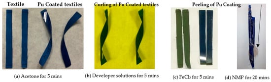
Figure 5.
Effect of solvent on screen-printed PU coating on fabric after immersion.
Figure 4 indicates that feature sizes down to 40 µm can be reliably etched on the PU-coated fabric, with linewidths and spacings of 10 µm also clearly defined. The yield and feature quality remain inadequate due to the poor adhesion of the copper film onto the interface layer, as indicated by the cracks in the patterns. The poor definition of the 10 µm copper squares further suggests that optimization of the fabrication process is required for higher resolutions.
4. Conclusions
This paper shows that microfabrication processes can be used in tandem with traditional screen-printing processes to reduce and improve form-factor and reliability of printed e-textiles, respectively. Feature sizes down to 10 µm have been realized on the PU-coated textile with this hybrid process. To achieve high yield and fine microcircuits, the defects and defect areas on the printed PU interface layer must be minimized. Furthermore, the adhesion of the thermally deposited films on the printed PU layer will need to improve to enhance reliability. Future work will also explore dry etching to mitigate the effect of solvents during fabrication.
Author Contributions
Conceptualization, A.K., M.G. and S.B.; methodology, A.K. and M.G.; design, investigation and formal analysis, A.K. and M.G.; writing—A.K. and M.G.; supervision, A.K. and S.B. All authors have read and agreed to the published version of the manuscript.
Funding
This research received no external funding.
Institutional Review Board Statement
Not applicable.
Informed Consent Statement
Not applicable.
Data Availability Statement
Not applicable.
Conflicts of Interest
The authors declare no conflict of interest.
References
- Komolafe, A. Reliability and Interconnections for Printed Circuits on Fabrics. Ph.D. Thesis, University of Southampton, Southampton, UK, 2016. [Google Scholar]
- Ohiri, K.A.; Pyles, C.O.; Hamilton, L.H.; Baker, M.M.; McGuire, M.T.; Nguyen, E.Q.; Currano, L.J. E-textile based modular sEMG suit for large area level of effort analysis. Sci. Rep. 2022, 12, 9650. [Google Scholar] [CrossRef] [PubMed]
- Dils, C.; Kalas, D.; Reboun, J.; Suchy, S.; Soukup, R.; Moravcova, D.; Schneider-Ramelow, M. Interconnecting embroidered hybrid conductive yarns by ultrasonic plastic welding for e-textiles. Textile Res. J. 2022, 92, 4501–4520. [Google Scholar]
- Stanley, J.; Hunt, J.A.; Kunovski, P.; Wei, Y. Novel Interposer for Modular Electronic Textiles: Enabling Detachable Connections between Flexible Electronics and Conductive Textiles. IEEE Sens. Lett. 2022, 6, 1–4. [Google Scholar] [CrossRef]
- Zysset, C.; Cherenack, K.; Kinkeldei, T.; Tröster, G. Weaving integrated circuits into textiles. In Proceedings of the International Symposium on Wearable Computers (ISWC) 2010, Seoul, Republic of Korea, 10–13 October 2010; pp. 1–8. [Google Scholar]
- Komolafe, A.; Torah, R.; Wei, Y.; Nunes-Matos, H.; Li, M.; Hardy, D.; Beeby, S. Integrating flexible filament circuits for e-textile applications. Adv. Mater. Technol. 2019, 4, 1900176. [Google Scholar] [CrossRef]


Disclaimer/Publisher’s Note: The statements, opinions and data contained in all publications are solely those of the individual author(s) and contributor(s) and not of MDPI and/or the editor(s). MDPI and/or the editor(s) disclaim responsibility for any injury to people or property resulting from any ideas, methods, instructions or products referred to in the content. |
© 2023 by the authors. Licensee MDPI, Basel, Switzerland. This article is an open access article distributed under the terms and conditions of the Creative Commons Attribution (CC BY) license (https://creativecommons.org/licenses/by/4.0/).