Proceeding Paper

Influence of Inductive Effect in Organic Residuals Content in IZO Thin Films and the Performance on the Behavior of MIS Capacitors on Plastic †

1
Centro de Investigaciones en Dispositivos Semiconductores, Instituto de Ciencias, Benemérita Universidad Autónoma de Puebla (BUAP), Puebla 72570, Mexico
2
Centro de Investigación en Biotecnología Aplicada (CIBA), Instituto Politécnico Nacional, Tlaxcala 72197, Mexico
*
Author to whom correspondence should be addressed.
Presented at the 1st International Conference on Micromachines and Applications, 15–30 April 2021; Available online: https://sciforum.net/conference/Micromachines2021.
Published: 14 April 2021
(This article belongs to the Proceedings of The 1st International Conference on Micromachines and Applications)

Abstract

:
In this work, zinc oxide and indium-doped zinc oxide thin films at different concentrations were deposited by solution techniques at 200 °C. The thin films were characterized by XRD, Raman, FTIR and the four-point probe technique. Through FTIR spectroscopy, interesting behavior was observed when the IZO film at 6 wt.% doping showed a lower number of organic residues. Due to an inductive effect, an unusual displacement of bonds was observed. The reduction of organic residuals corroborated with the behavior of flexible metal–insulator–semiconductor (MIS) capacitors.

1. Introduction

Metal oxide semiconductors are materials that provide good stability, high transparency in the visible region, high conductivity and are easily handled to be implemented in polymeric substrates to flexible electronics applications [1]. Another interesting aspect of metal oxide semiconductors is their deposition by solution processes such as spin-coating and spray pyrolysis. These low-cost techniques provide good uniformity and good quality of the films [2,3]. For the formation of metal oxide semiconductors, four phases occur in solution processes: (1) the synthesis or generation of precursor solution, (2) deposition, (3) pyrolysis or condensation and (4) crystallization. Usually, the low temperature requirements of Steps 3 and 4 are 200–400 and 400 °C, respectively [4]. During the process, when implementing PET as a substrate, it is necessary to use temperatures of approximately 200 °C or less, because a higher temperature is incompatible with the substrate. However, the use of low temperatures in this range limits the decomposition of the precursor solution, and thin films are formed with organic residues that act as traps and defects, resulting in poor electrical properties of the films. Zinc oxide is one of the most common oxide semiconductors implemented in solution processes [5]. In this work, the synthesis of indium-doped zinc oxide (IZO) thin films at different doping concentrations was obtained at 200 °C. In a ternary compound (Tuz+Mvm+Xxq−), the tentative estimation of the inductive effect of T on the M–X bond or substitution of a metal can be known from the electronegativity difference between the Tz+ and Mm+ cations and results in the redistribution of the electron density [6,7].

2. Materials and Methods

The precursor solutions were prepared using 0.2 M zinc acetate dihydrate (Zn(AcO2)·2H2O) (99.9%, Sigma-Aldrich) dissolved in 2-methoxyethanol (2-ME) and methylenamine (MEA) to obtain ZnO thin film and In(NO3)3·xH2O at 1, 3, 6 and 9 wt.% mixed in the ZnO solutions to obtain IZO thin films. The solutions were deposited by spin-coating at 3000 rpm for 30 s on silicon wafers and corning glass 2947 as substrates, and the samples were placed on a hot plate at 200 °C for 4 h to form the thin films.
The metal–insulator–semiconductor (MIS) capacitors were fabricated using ITO-coated PET substrates (Sigma-Aldrich). As dielectric film, spin-on-glass (SOG) solution was prepared with a mixture of 33% LSF47-SOG solution in 66% LSFD1 diluent, then it was spin-coated at 3000 rpm for 30 s and cured for 1.5 h at 200 °C. The ZnO and IZO thin films were used as semiconductors. Finally, as top contact, ITO precursor solution was prepared using 0.3 M InCl3·xH2O and SnCl2·xH2O at 5 wt.% diluted in methanol, then it was sprayed on top of the semiconductor film through a shadow mask and using a homemade high-frequency ultrasonic spray pyrolysis deposition system (Citizen, Cun60) with an ultrasonic transducer operating at 2.5 MHz and air as carrier gas at a 0.7 mL/min flow rate for 10 min at 200 °C. For the characterization of the semiconductor thin films, a Discover X-ray diffractometer (D8 Bruker AXS), micro-Raman (LabRAM HR spectrometer), FTIR spectroscopy (Bruker Vertex-70) and the four-point probe technique (Thorlabs Pro 4–4000) were used. For the MIS capacitors, the measurement was performed using a Keithley-4200 semiconductor characterization system under dark conditions, ambient air and room temperature with forward and reverse sweeps with 0.1 V steps, 30 mV AC voltage and 10 kHz frequency.

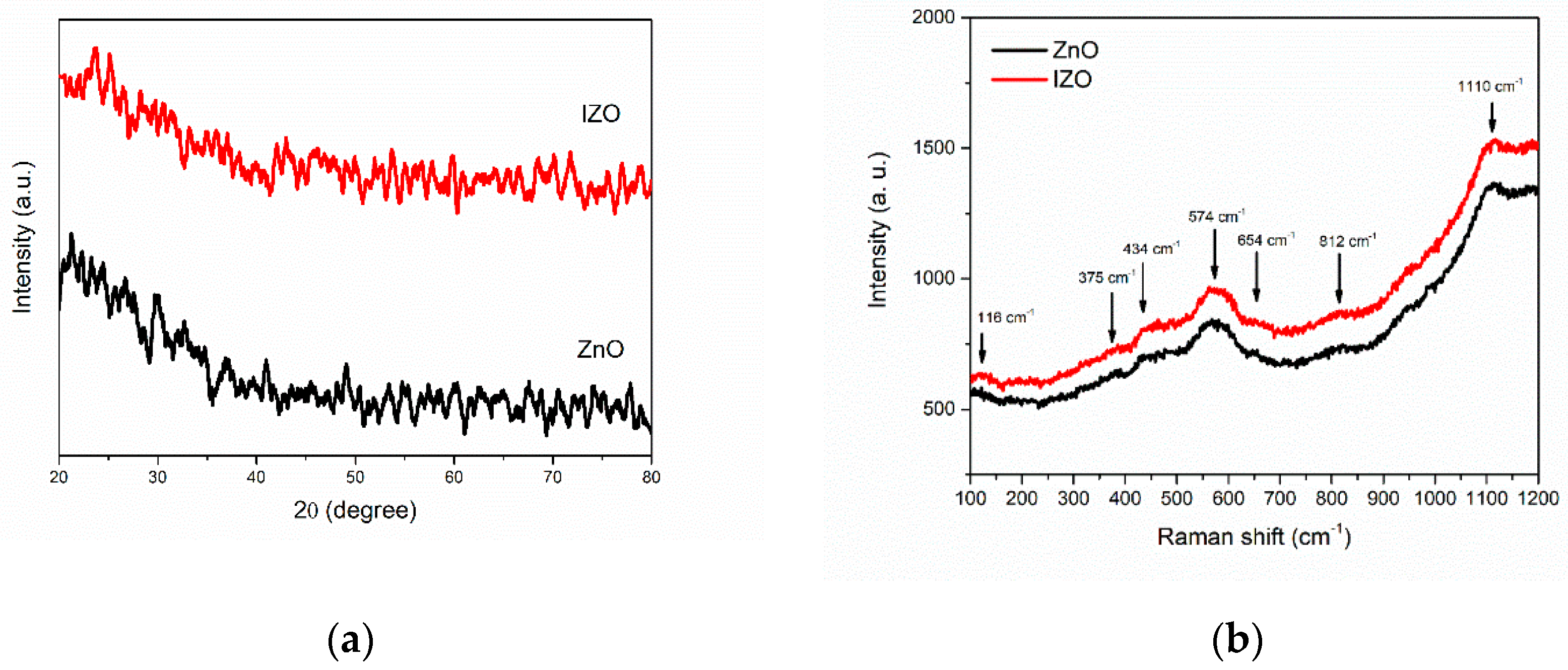
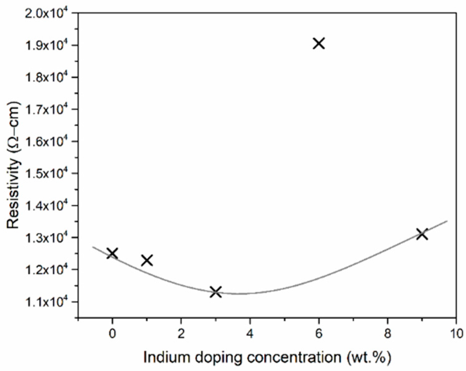
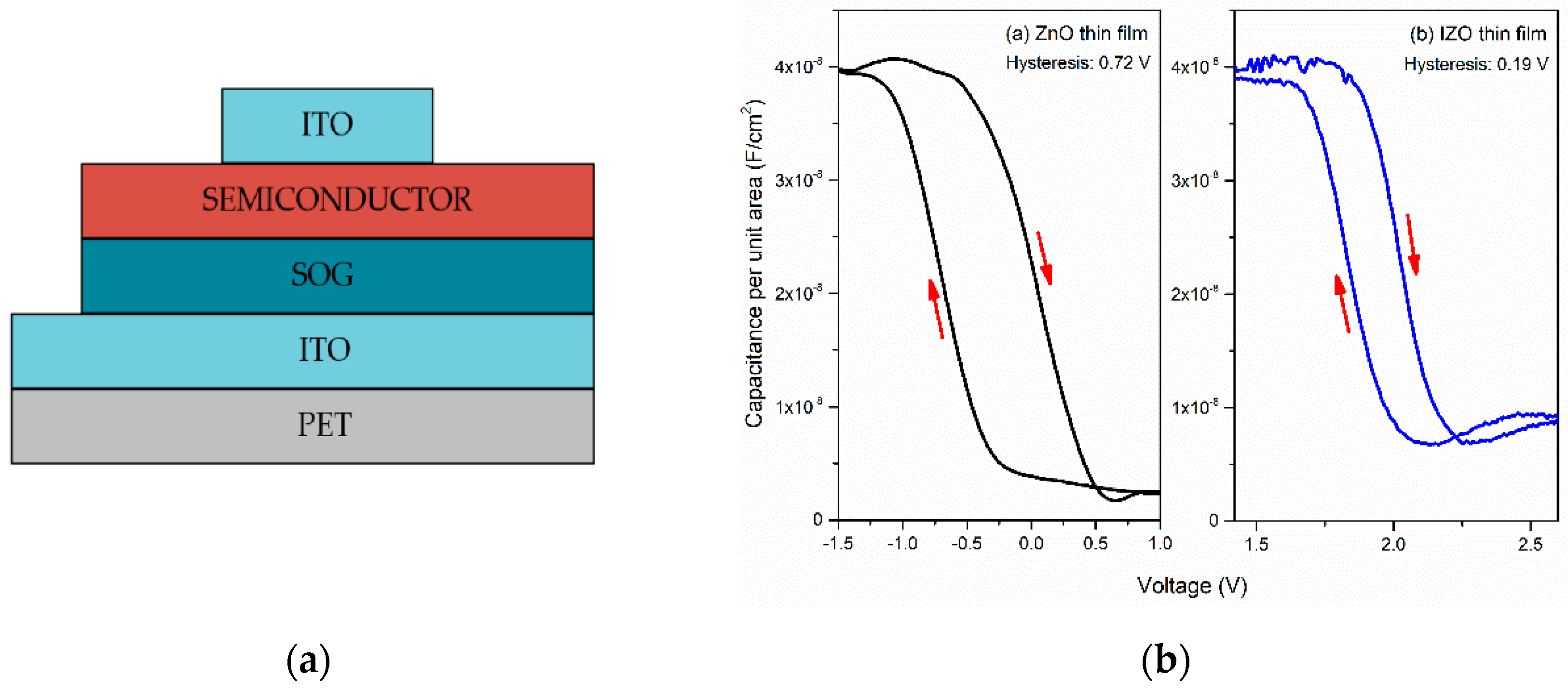
3. Results and Discussion

Figure 1 shows the structural characteristics of the ZnO and IZO thin films. Figure 1a shows that doped and undoped thin films have amorphous structures and do not change with the dopant addition. This characteristic is commonly reported in oxide semiconductors [8]. Figure 1b shows the Raman spectra of the films where vibrational modes were found at 116, 374, 434, 573, 654, 812 and 1110 cm−1 corresponding to modes E2(low), A1(TO), E2(high), E1(LO), E1(TA+LO), E2(high)-E2(low) and A1(2LO), respectively [9,10,11,12,13]. The E2(low) mode is associated with vibrations of the Zn sublattice, and the high E2(high) mode is caused by vibration of oxygen atoms, whereas the E1(LO) mode is related to the vibrations of Zn atoms [9]. As mentioned, A1 and E1 modes are assigned to a polar branch [13]. For the IZO film, no significant changes were observed.
The FTIR spectra of the ZnO and IZO thin films are shown in Figure 2. For the ZnO thin film, the stretching modes of Zn-O at 428 and 572 cm−1 were observed [14,15,16]. At 677 cm−1, the COO- bond related to the overlapping of σ and π of the ligand was found [17,18]. Finally, symmetric (1421 cm−1) and asymmetric (1531 cm−1) C-O bonds and O-H groups were observed at 1636 cm−1 [14,19]. The origin of the COO-, C-O and O-H bonds are related to the low decomposition of the precursor solution [15]. On the one hand, the presence of these organic residues, such as the C-O bonds, can generate disorder in the film structure and cause surface defects [20,21]. On the other hand, the hydroxyl group plays a role as a charge trap due to its polar nature [18,22]. For the IZO thin films, similar bonds were observed. In addition, Figure 2 shows the calculated areas of the residual groups for all the films. A reduction in the intensity of the bands related to the defects was found for the sample doped at 6 wt.%. In this sample, the Zn-O bond shifts at 583 cm−1. This may be due to the fact that the doping concentration may favor the inductive effect by the substitution of Zn2+ by In3+. The inductive effect is due to the difference in electronegativity of the atoms bonded together. The polarization of the bond causes the appearance of partial charges +δ and -δ, which have effects on the neighboring bonds at a relatively short distance [23]. Thus, the bonding electrons will tend to move toward the atom of greater electronegativity; as the electron density shifts toward that atom, it will become negative and tend to attract fewer electrons [7].
Figure 3 shows the resistivities of the undoped and doped thin films. The resistivity exhibits a trend similar to those typically reported. Interestingly, for the IZO film doped at 6 wt.%, an increase in the resistivity was observed. This behavior can be correlated with the FTIR results, where it was observed that the bonds related to the organic residuals are reduced at the lowest values for this sample. This reduction of C-O, COO- and O-H bonds decreases the correlated free carrier concentration, increasing the resistivity. Moreover, this behavior may be related to the inductive effect previously mentioned.
In addition to the resistivity variation, a change was observed in the C–V characterization of the MIS capacitors (Figure 4). Figure 4a shows the MIS capacitor structure. Figure 4b shows the C–V curves, and the typical accumulation and depletion characteristic regions for an MIS capacitor are observed. When the C–V characteristics were measured, forward and reverse sweeps were applied to evaluate the hysteresis. The origin of hysteresis occurs by the existence of organics groups inside the semiconductor. The reduction of the hysteresis, from the ZnO (0.72 V) to the IZO (0.10 V) film, is the result of the decrease in organic residues present in the IZO film at 6 wt.%. The hysteresis is closely associated with interface trap states in oxide semiconductor films [24,25]. The hysteresis reduction observed in the capacitor with the IZO film indicates that the film with the least amount of organic residues allows better electrical performance due to the reduction of traps present in the film.

4. Conclusions

In this work, it was observed that the concentration of dopant in ZnO contributes to the electrical behavior of the films obtained, favoring the reduction of organic residues. It was also observed that the reduction of the bond between metal and ligand can contribute to the variation of the semiconductor properties due to a possible redistribution of the density of states due to the addition of dopant. In the fabricated MIS capacitors, an improvement in the characteristics of the C–V curve was observed with the IZO film used as the active layer.

Funding

This research was funded by Fondo Sectorial de Investigación para la Educación CONACyT-SEP (Grant Number: A1-S-7888) and VIEP-BUAP (Grant Number: DJMA-EXC17-G).

Data Availability Statement

Data is contained within the article.

Conflicts of Interest

The authors declare no conflict of interest.

References

  1. Jo, J.-W.; Kang, S.-H.; Heo, J.S.; Kim, Y.-H.; Park, S.K. Flexible metal oxide semiconductor devices made by solution methods. Chem. Eur. J. 2020, 26, 9126. [Google Scholar] [CrossRef] [PubMed]
  2. Jilani, A.; Abdel-wahab, M.S.; Hammad, A.H. Advance deposition techniques for thin film and coating, modern technologies for creating the thin-film systems and coatings. Mod. Technol. Creat. Thin-Film Syst. Coat. 2017, 2, 137–149. [Google Scholar] [CrossRef]
  3. Leng, J.; Wang, Z.; Wang, J.; Wu, H.-H.; Yan, G.; Li, X.; Guo, H.; Liu, X.; Zhang, Q.; Guo, Z. Advances in nanostructures fabricated via spray pyrolysis and their applications in energy storage and conversion. Chem. Soc. Rev. 2019, 48, 3015–3072. [Google Scholar] [PubMed]
  4. Bretos, I.; Jiménez, R.; Ricote, J.; Calzada, M.L. Low-temperature solution approaches for the potential integration of ferroelectric oxide films in flexible electronics. IEEE Trans. Ultrason. Ferroelectr. Freq. Control 2020, 67, 1967–1979. [Google Scholar] [CrossRef] [PubMed]
  5. Cheong, K.Y.; Mohammed, N.; Ramanan, S. Electrical and optical studies of ZnO:Ga thin films fabricated via the sol–gel technique. Thin Solid Films 2002, 410, 142–146. [Google Scholar] [CrossRef]
  6. Kuznetsov, D.A.; Han, B.; Yu, Y.; Rao, R.R.; Hwang, J.; Román-Leshkov, Y.; Shao-Horn, Y. Tuning redox transition via inductive effect in metal oxides and complexes, and implications in oxygen electrocatalysis. Joule 2018, 2, 225–244. [Google Scholar] [CrossRef]
  7. Etourneau, J.; Portier, J. The role of the inductive effect in solid state chemistry how the chemist can use it to modify both the structural and the physical properties of the materials. J. Alloys Compd. 1992, 188, 1–7. [Google Scholar] [CrossRef]
  8. Lee, S.Y. Comprehensive review on amorphous oxide semiconductor thin film transistor. Trans. Electr. Electron. Mater. 2020, 21, 235–248. [Google Scholar] [CrossRef]
  9. Lee, J.-H.; Oh, K.; Jung, K.; Wilson, K.C.; Lee, M.-J. Tuning the morphology and properties of nanostructured Cu-ZnO thin films using a two-step sputtering technique. Metals 2020, 10, 437. [Google Scholar] [CrossRef]
  10. Oliveira, A.G.; Andrade, J.d.L.; Montanha, M.C.; Lima, S.M.; da Cunha Andrade, L.H.; Winkler Hechenleitner, A.A.; Gómez Pineda, E.A.; Fernandes de Oliveira, D.M. Decontamination and disinfection of wastewater by photocatalysis under UV/visible light using nano-catalysts based on Ca-doped ZnO. J. Environ. Manag. 2019, 240, 485–493. [Google Scholar] [CrossRef]
  11. Santhosh Kumar, A.; Huang, N.M.; Nagaraja, H.S. Influence of Sn doping on photoluminescence and photoelectrochemical properties of ZnO nanorod arrays, Electron. Mater. Lett. 2014, 10, 753–758. [Google Scholar] [CrossRef]
  12. Medjaldi, M.; Touil, O.; Boudine, B.; Zaabat, M.; Halimi, O.; Sabais, M.; Ozyuzer, L. Study of undoped and indium doped ZnO thin films deposited by sol gel method. Silicon 2018, 10, 2577–2584. [Google Scholar] [CrossRef]
  13. Cuscó, R.; Alarcón-Lladó, E.; Ibáñez, J.; Artús, L.; Jiménez, J.; Wang, B.; Callahan, M.J. Temperature dependence of Raman scattering in ZnO. Phys. Rev. B. 2007, 75, 165202. [Google Scholar] [CrossRef]
  14. Dominguez, M.A.; Martinez, J.; Monfil-Leyva, K.; Soto, S.; Netzahualcoyolt, C.; Moreno, M. Incorporation of ZnO nanoparticles on solution processed zinc oxide thin-film transistors. Trans. Electr. Electron. Mater. 2018, 19, 412–416. [Google Scholar] [CrossRef]
  15. Adamopoulos, G.; Bashir, A.; Gillin, W.P.; Georgakopoulos, S.; Shkunov, M.; Baklar, M.A.; Stingelin, N.; Bradley, D.D.C.; Anthopoulos, T.D. Structural and electrical characterization of ZnO films grown by spray pyrolysis and their application in thin-film transistors. Adv. Funct. Mater. 2011, 21, 525–531. [Google Scholar] [CrossRef]
  16. Adamapoulos, G.; Bashir, A.; Wöbkenberg, P.W.; Bradley, D.D.C.; Anthopoulos, T.D. Electronic properties of ZnO field-effect transistors fabricated by spray pyrolysis in air ambient. Appl. Phys. Lett. 2009, 95, 133507. [Google Scholar] [CrossRef]
  17. Gonçalves, A.S.; Marques de Lima, S.A.; Davolos, M.R. Gallium-doped zinc oxide prepared by the Pechini method. Eclet. Quím. 2001, 27, 293–304. [Google Scholar] [CrossRef]
  18. Ahn, B.D.; Jeon, H.-J.; Sheng, J.; Park, J.; Park, J.-S. A review on the recent developments of solution processes for oxide thin films transistors. Semicond. Sci. Technol. 2015, 30, 064001. [Google Scholar] [CrossRef]
  19. Dominguez, M.A.; Orduña-Diaz, A. Fully solution-processed zinc oxide MIS capacitors by ultrasonic spray pyrolysis in air ambient. J. Appl. Res. Technol. 2017, 15, 278–282. [Google Scholar] [CrossRef]
  20. Saha, J.K.; Bukke, R.N.; Mude, N.N.; Jang, J. Significant improvement of spray pyrolyzed ZnO thin film by precursor optimization for high mobility thin film transistors. Sci. Rep. 2020, 10, 8999. [Google Scholar] [CrossRef]
  21. Todorov, T.; Hillhouse, H.W.; Aazou, S.; Sekkat, Z.; Vigil-Galán, O.; Deshmukh, S.D.; Agrawal, R.; Bourdais, S.; Valdés, M.; Arnou, P.; et al. Solution-based synthesis of kesterite thin film semiconductors. J. Phys. Energy. 2020, 2, 012003. [Google Scholar] [CrossRef]
  22. Hennek, J.W.; Smith, J.; Yan, A.; Kim, M.-G.; Zhao, W.; Dravid, V.P.; Facchetti, A.; Marks, T.J. Oxygen “getter” effects on microstructure and carrier transport in low temperature combustion-processed a-InXZnO (X = Ga, Sc, Y, La) transistors. J. Am. Chem. Soc. 2013, 135, 10729–10741. [Google Scholar] [CrossRef] [PubMed]
  23. Barret, R. Importance and Evaluation of the pKa. In Therapeutical Chemistry, 1st ed.; Barret, R., Ed.; Elsevier: Amsterdam, The Netherlands, 2018; pp. 21–51. [Google Scholar]
  24. Zeumault, A.; Subramanian, V. Use of high-k encapsulation to improve mobility in trap-limited metal-oxide semiconductors. Phys. Status Solidi B 2017, 254, 1700124. [Google Scholar] [CrossRef]
  25. Song, Y.; Katsman, A.; Butcher, A.L.; Paine, D.C.; Zaslavsky, A. Temporal and voltage stress stability of high performance indium-zinc-oxide thin film transistors. Solid State Electron. 2017, 136, 43–50. [Google Scholar] [CrossRef]
Figure 1. Structural characterization: (a) XRD pattern of the amorphous ZnO and IZO thin films; (b) Raman spectra for the ZnO and IZO thin films. No significant variations are observed in the doped thin film.
Engproc 04 00009 g001
Figure 2. FTIR characterization: (a) FTIR of ZnO thin film. High intensity of the bands of the organic residues COO-, C-Osym, C-Oasym and O-H groups is observed; (b) FTIR of IZO thin films. The insets show the shift of the identified Zn-O bond at 583 cm−1 due to an inductive effect due to the doping at 6 wt.%.
Engproc 04 00009 g002
Figure 3. Resistivity of the doped thin films at different concentrations. The line shows the usual dependence of the resistivity. The film doped at 6 wt.% shows an irregular increase.
Engproc 04 00009 g003
Figure 4. MIS capacitor characterization: (a) schematic MIS capacitor structure; (b) metal–insulator–semiconductor (MIS) capacitor with (a) ZnO and (b) IZO thin films. The hysteresis parameter found was (a) 0.72 and (b) 0.19 V. The reduction of the hysteresis of the doped film is attributed to the reduction of traps originated by organic residues.
Engproc 04 00009 g004
Publisher’s Note: MDPI stays neutral with regard to jurisdictional claims in published maps and institutional affiliations.

