Abstract
The electrochemical cell is designed with a conductive substrate (working electrode) where deposition takes place within a three-electrode cell. In order to complete the electrochemical circuit, the cell has been equipped with a counter electrode (CE) and a reference electrode (RE). The cell additionally incorporates an AFM probe, which serves as a scanning instrument for characterizing the deposited structures as well as a localized contact for triggering the electrochemical processes. The materials used in the cell components are chosen with care to ensure compatibility with the electrolyte solution and to minimize interference or contamination. The aim of this study is to design an electrochemical cell for in situ real-time monitoring of deposition using Atomic Force Microscopy (AFM), facilitating the controlled growth of thin films or nanostructures on a conducting substrate. The combination of AFM and electrochemical deposition allows for real-time monitoring and precise manipulation of the growth process at the nanoscale. This research focuses on the key design considerations and optimization parameters for an effective electrochemical cell that enables the in situ characterization and control of the deposition process.
1. Introduction
In real-time, the deposition process is tracked using in situ Atomic Force Microscopy (AFM) monitoring and characterization techniques, such as tapping mode. AFM’s remarkable high-resolution-imaging capabilities enable the observation of surface topography, grain structure, and growth kinetics of the deposited structures. By aligning the findings from AFM with the electrochemical parameters, a comprehensive understanding of the growth mechanism and the relationships between structure and properties can be attained.
The creation of an efficient electrochemical cell designed specifically for in situ AFM deposition opens up new avenues for investigating electrochemical processes on a nanoscale. This synergy of precise control over deposition conditions and real-time-imaging capabilities provides valuable insights into the mechanisms governing growth. It also sets the stage for the development and production of advanced functional materials with customized properties suited for diverse applications.
AFM belongs to the category of scanning probe techniques. Unlike electron microscopes, AFM has the versatility to operate under various conditions, including ambient environments [1,2,3], in liquids [4,5,6,7,8,9,10,11,12,13,14], and even in gaseous environments. AFM serves multiple functions beyond just imaging; it can also be employed for lithography, spectroscopy, and nanomanipulation.
The symmetry of the electric field distribution holds significant importance in electrochemical cells due to its direct association with the precision of electrochemical measurements. To illustrate, the arrangement of current lines can exert a critical influence on the electrochemical processes occurring within a cell. More specifically, regions of the electrode featuring a supervisor current density may be more susceptible to accelerated degradation compared to their counterparts with lower current density. In numerous electrochemical systems, understanding the distribution of current density serves the dual purpose of either reducing measurement errors or mitigating undesirable effects, such as the non-uniform deposition seen in electrochemical deposition processes and the non-uniform deterioration of electrodes.
This study investigates the simulation of potential distribution within an electrochemical cell designed for Atomic Force Microscopy (AFM) in an electrochemical context. This specific cell was devised for the deposition of Bismuth nanoparticles. The primary motivation behind the new cell design is to facilitate the simultaneous measurement of variations in the surface topography of electrochemically deposited films while maintaining precise control over the applied potential, thereby minimizing measurement errors. The objective of simulating the electric field distribution in these electrochemical cells is to gain insights into how electrical potentials are distributed within the electrolyte medium.
2. Materials and Methods
2.1. Electric Field Simulation Setup inside the Cell
A commercial finite element software, COMSOL Multiphysics 3.5 ™ [12], was utilized to perform a three-dimensional simulation. Initially, the cell’s geometry was replicated in a 3D model, depicted in Figure 1a. The electrolyte was represented as a cylindrical structure containing both anode and cathode electrodes (Figure 1b). The working electrode (Figure 1b, red) was in contact with the electrolyte on a single surface, while the counter electrode (Figure 1b, blue) was emulated with a metal ring placed within the electrolyte cylinder. The research focused on the primary current due to its dependence on electrode geometry and arrangement.
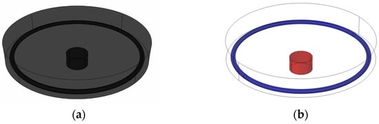
Figure 1.
The electrochemical cell: (a) cell’s 3D schematic; (b) schematic of the cell’s geometry for simulation, the working electrode is represented by the red part, and the counter electrode is represented by the blue part.
In scenarios involving primary current distribution, rapid kinetics were assumed. This allowed for simplification where the potential of the electrolyte nearby the electrode is matched to the applied electrode potential. The Finite Element Method (FEM) was employed to solve Ohm’s law and Laplace equations at various points distributed within the electrolyte. More comprehensive information can be found in our earlier publication.
The meshing strategy involved selecting meshes with finely detailed boundaries between the electrolyte and the electrodes interface, with a thickness of 20 nm. As a result, each cell’s meshing employed 450,000 elements. The meshing concept for the cells is depicted in Figure 2.
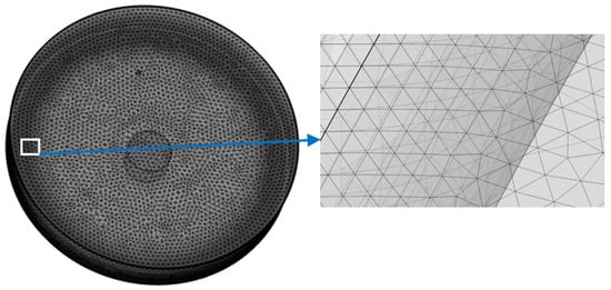
Figure 2.
The meshing of the domains in cell: left: The cell is meshed into 450,000 elements with very fine meshing near the electrodes; right: a zoom in of the meshes near the counter electrode.
2.2. Materials
A solution containing a known amount of bismuth ions (1000 mg per liter of Bi(III)) dissolved in HNO3 was bought from Merck. Analytical-grade acetic acid (CH3COOH) and 99.99% pure platinum wire were obtained from Sigma Aldrich. A glassy carbon disk electrode (GCE), which had a 12 mm outer diameter and a 5 mm disk diameter, was purchased from Pin research.
2.3. Electrochemical Cell Preparation
The electrochemical cell was subjected to a thorough cleaning process involving sequential 15 min ultrasonic baths in acetone, isopropanol alcohol, and Milli-Q water. Prior to affixing the glassy carbon electrode (GCE) to the electrochemical cell, the electrode underwent polishing using Al2O3 powder and nylon polishing pads. Subsequently, it was rinsed with Milli-Q water. The platinum wire served as the counter electrode and was positioned in a circular manner within the inner frame of the cell. Additionally, a typical Ag/AgCl/NaCl (3M) reference electrode from BASi was utilized. Once the electrodes were properly placed within the cell, they were wired to a PalmSense 4 potentiostat.
2.4. AFM Electrochemical Deposition
Once the electrodes were introduced into the electrochemical cell, a solution containing the analyte (at a concentration of 1 mg L−1 of Bi(III) in a 0.5 M acetate buffer solution) was introduced into the cell. Subsequently, the working electrode was subjected to scanning using the Agilent 5500 Atomic Force Microscope (AFM), which was operated in tapping mode. A MikroMasch tip was used to scan the electrode. The tip possessed a force constant of 5 N/m, a length of 125 μm, and was coated with gold. The scanning process was conducted at a frequency of 1 Hz, covering a scanning area of 10 × 10 μm2. The area of interest was first scanned at open circuit potential, and then a voltage of −1.0 V vs. Ag/AgCl/NaCl (3M) was imposed for 100 s.
3. Results and Discussion
3.1. Electric Field Simulation inside the Cell
To facilitate a comprehensive understanding of the potential distribution, Figure 3 presents a visualization of the simulated potential within the cell. In Figure 3a, it is evident that the electrical field exhibits a symmetrical distribution within the electrolyte, forming concentric patterns around the working electrode. However, critical observation arises when we consider Figure 3b, where the geometry of the counter electrode has been meticulously chosen. In this case, a ring-shaped counter-electrode configuration has been employed, leading to a notable enhancement in the field’s focus and intensity in close proximity to the working electrode. This configuration optimizes the electrochemical performance and efficiency of the cell, making it a compelling choice for various applications.
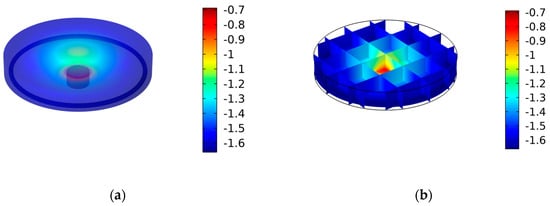
Figure 3.
The electric field distribution within the cell with false scale bars in V: (a) 3D distribution of the potential inside the cell; (b) electric field cross slices inside the cell.
3.2. AFM Electrochemical Deposition
To commence the electrochemical analysis, the initial step involved injecting the solution into the electrochemical cell. Subsequently, the tip of the apparatus was carefully positioned near the surface of the electrode to facilitate scanning. In Figure 4, AFM images illustrate the state of the glassy carbon electrode (GCE) and the features that have formed on its surface.
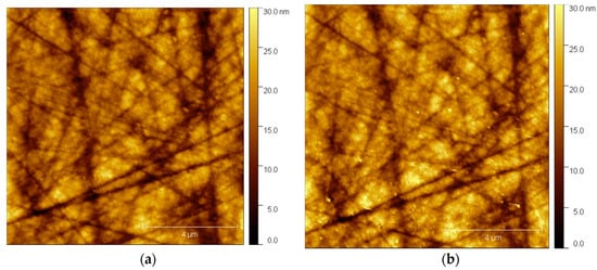
Figure 4.
Imaging of the in situ deposited nanoparticles using AFM. (a) Scan of the surface at OCP; (b) scan of the surface at −1.00 V vs. Ag/AgCl/NaCl (3M) for 100 s.
Figure 4a provides a detailed view of the GCE’s surface. Notably, there are no discernible deposits or foreign substances present on the glassy carbon substrate, with the only visible markings being attributed to the minor scratches incurred during the polishing process.
Following this preliminary assessment, a cathodic voltage of −1.0 V/Ag/AgCl/NaCl (3M) was introduced to the glassy carbon electrode (GCE). This electrochemical treatment was sustained for a duration of 60 s, serving as a critical component of the experimental procedure to initiate specific electrochemical processes and investigate the resultant effects on the electrode’s upper face (Figure 4b).
4. Conclusions
The newly constructed cell was especially intended to allow the simultaneous measuring of electrochemically deposited bismuth nanostructures. This novel cell design allows for accurate monitoring of bismuth nanostructure deposition and improves our capability to collect real-time data during the electrochemical process. With this improved cell, we could obtain a better knowledge of bismuth nanostructure production and electrochemical behavior, opening up new avenues for in-depth study and analysis in this field. The 3D FEM simulations have revealed that the proposed cell design results in an even distribution of electric potential throughout the electrolyte. The synergy between AFM and electrochemistry constitutes a potent methodology for gaining insights into the electrochemical developments occurring on the conductive substrate’s top surface. The ability to directly observe the creation of a bismuth film, even when it is present in low concentrations, is made possible through in situ AFM measurements conducted within the solution. When a cathodic voltage of −1.00 V was applied for a duration of 100 s, the initiation of bismuth film formation manifested as nanostructures resembling nanoparticle features.
Author Contributions
Conceptualization, A.K.; methodology, A.K.; formal analysis, A.K.; investigation, A.K.; writing—original draft preparation, A.K.; writing—review and editing, A.K. and M.A.S. All authors have read and agreed to the published version of the manuscript.
Funding
This work was partially sponsored by the Slovenian Research Agency (Research Programs P1-0034).
Institutional Review Board Statement
Not applicable.
Informed Consent Statement
Not applicable.
Data Availability Statement
Data are contained within the article.
Conflicts of Interest
The authors declare no conflicts of interest.
References
- Kreta, A.; Rodošek, M.; Slemenik Perše, L.; Orel, B.; Gaberšček, M.; Šurca Vuk, A. In situ electrochemical AFM, ex situ IR reflection-absorption and confocal Raman studies of corrosion processes of AA 2024-T3. Corros. Sci. 2016, 104, 290–309. [Google Scholar] [CrossRef]
- Kreta, A.; Pavlica, E.; Božič, M.; Bratina, G. Nanoscopic Roughness Characterization of Chitosan with Buried Graphene Oxide for Fuel Cell Application. Eng. Proc. 2022, 31, 26. [Google Scholar] [CrossRef]
- Kreta, A.; Swillam, M.A.; Guirguis, A.; Hassanien, A. Unbundling SWCNT Mechanically via Nanomanipulation Using AFM. Eng. Proc. 2023, 56, 83. [Google Scholar] [CrossRef]
- Kreta, A.; Gaberšček, M.; Muševič, I. Time-resolved in situ electrochemical atomic force microscopy imaging of the corrosion dynamics of AA2024-T3 using a new design of cell. J. Mater. Res. 2021, 36, 79–93. [Google Scholar] [CrossRef]
- Chhikara, M.; Pavlica, E.; Bratina, G. Grafold-driven nucleation of pentacene on graphene. Surf. Sci. 2013, 609, L5–L8. [Google Scholar] [CrossRef]
- Chhikara, M.; Pavlica, E.; Matković, A.; Beltaos, A.; Gajić, R.; Bratina, G. Pentacene on graphene: Differences between single layer and bilayer. Carbon 2014, 69, 162–168. [Google Scholar] [CrossRef]
- Arman, A.; Ţălu, Ş.; Luna, C.; Ahmadpourian, A.; Naseri, M.; Molamohammadi, M. Micromorphology characterization of copper thin films by AFM and fractal analysis. J. Mater. Sci. Mater. Electron. 2015, 26, 9630–9639. [Google Scholar] [CrossRef]
- Sheikh, K.H.; Giordani, C.; Kilpatrick, J.I.; Jarvis, S.P. Direct submolecular scale imaging of mesoscale molecular order in supported dipalmitoylphosphatidylcholine bilayers. Langmuir 2011, 27, 3749–3753. [Google Scholar] [CrossRef] [PubMed]
- Dinmohammadi, M.; Ghodsi, F.E. Effect of PEG/CTAB on capacitive performance of α-Fe2O3-CuO nanocomposite electrode. J. Sol-Gel Sci. Technol. 2023, 108, 827–839. [Google Scholar] [CrossRef]
- Kreta, A.; Hočevar, S.B. An In Situ AFM Study of Electrochemical Bismuth Film Deposition on a Glassy Carbon Substrate Electrode Using a Low Concentration of Bismuth Ions. Eng. Proc. 2022, 31, 27. [Google Scholar] [CrossRef]
- Dickinson, E.J.F.; Ekström, H.; Fontes, E. COMSOL Multiphysics®: Finite element software for electrochemical analysis. A mini-review. Electrochem. Commun. 2014, 40, 71–74. [Google Scholar] [CrossRef]
- Fanijo, E.O.; Thomas, J.G.; Zhu, Y.; Cai, W.; Brand, A.S. In situ quantitative topographic measurement and corrosion behaviour of low carbon steel in chloride solutions. Corros. Eng. Sci. Technol. 2023, 58, 599–613. [Google Scholar] [CrossRef]
- Chen, H.; Qin, Z.; He, M.; Liu, Y.; Wu, Z. Application of Electrochemical Atomic Force Microscopy (EC-AFM) in the Corrosion Study of Metallic Materials. Materials 2020, 13, 668. [Google Scholar] [CrossRef] [PubMed]
- Yasakau, K. Application of AFM-Based Techniques in Studies of Corrosion and Corrosion Inhibition of Metallic Alloys. Corros. Mater. Degrad. 2020, 1, 345–372. [Google Scholar] [CrossRef]
Disclaimer/Publisher’s Note: The statements, opinions and data contained in all publications are solely those of the individual author(s) and contributor(s) and not of MDPI and/or the editor(s). MDPI and/or the editor(s) disclaim responsibility for any injury to people or property resulting from any ideas, methods, instructions or products referred to in the content. |
© 2023 by the authors. Licensee MDPI, Basel, Switzerland. This article is an open access article distributed under the terms and conditions of the Creative Commons Attribution (CC BY) license (https://creativecommons.org/licenses/by/4.0/).