
Photoresponsivity Enhancement of SnS-Based Devices Using Machine Learning and SCAPS Simulations †


1
Laboratoire Electronique Avancée (LEA), Department of Electronics, University of Batna 2, Batna 05000, Algeria
2
Laboratory of Automation and Manufacturing Engineering, University of Batna 2, Batna 05000, Algeria
3
Institut Sciences Techniques Appliquées (ISTA), University of Larbi Ben M’hidi, Oum El Bouaghi 04000, Algeria
*
Author to whom correspondence should be addressed.
†
Presented at the 10th International Electronic Conference on Sensors and Applications (ECSA-10), 15–30 November 2023; Available online: https://ecsa-10.sciforum.net/.
Eng. Proc. 2023, 58(1), 128; https://doi.org/10.3390/ecsa-10-16014
Published: 15 November 2023
(This article belongs to the Proceedings of The 10th International Electronic Conference on Sensors and Applications)
Abstract
:In this work, we propose a novel alternative design technique based on combined SCAPS numerical simulations and Machine Learning (ML) computation to improve the photocurrent performances for efficient eco-friendly optoelectronic applications. In this context, a new SnS absorber structure based on introducing gold (Au) nanoparticles (NPs) is proposed. It is revealed that the proposed design framework can predict the best spatial distribution of Au NPs, allowing for the enhanced optical behavior of SnS absorber film. This can pave the way for the optoelectronic systems designers to identify the geometry and the appropriate material for each layer of the device. Moreover, the results of the proposed SnS-based structure offer an innovative approach for the elaboration of eco-friendly, high-efficiency thin-film optoelectronics devices that is more promising than the previously reported designing techniques.
1. Introduction
Photodetectors hold a prominent role in optoelectronic devices as they possess the capacity to convert optical signals into electrical signals. They find applications in various fields, including early missile threat detection, optical communication, environmental monitoring, water purification, flame detection, ultraviolet astronomy, environmental surveillance, remote sensing, biomedicine, and photography [1,2,3]. In these circumstances, various materials like perovskites, monolayers, colloidal quantum dots, and solution-processable substances have been extensively investigated with the goal of addressing the primary challenges associated with conventional photodetectors [3,4]. Particularly, tin sulfide (SnS) stands out as a highly promising material. It is characterized by its non-toxic properties, chemical stability, Earth abundance, high carrier mobility, visible light-absorption ability, low recombination velocity, and a tunable direct bandgap [3,5]. These attributes collectively position SnS as an exceptional candidate for high-performance optoelectronic devices. In addition, tin sulfide encompasses various phases, including SnS, Sn2S3, SnS2, Sn3S4, and Sn4S5, each characterized by distinct stoichiometric ratios of tin and sulfur. The synthesis and doping of these diverse SnS phases are achievable through various methods, such as pulse electrodeposition (PED), spray pyrolysis, physical vapor deposition (PVD), plasma-enhanced chemical vapor deposition (PECVD), chemical bath deposition (CBD), electron beam evaporation (EBM), atomic layer deposition (ALD), and RF magnetron sputtering [3,4,5,6,7]. While certain SnS photodetectors have exhibited a noteworthy performance, their achieved results still fall short of expectations. Moreover, the SnS alloys are not free from disadvantages. One of which is their low resistance to the aggressive influence of environmental factors such as temperature, oxygen, and electromagnetic radiation. With that, there are new different classes of sulfide-based materials with good electronic properties, which have been developed using appropriate experimental facilities [8,9]. To address this challenge, noble metal nanoparticles can be introduced in the SnS absorber layer. This can enhance the photodetector optoelectronic properties through improving light absorption and generating plasmonic effects. Nonetheless, in the domain of thin-film semiconductor devices, a persistent iterative optimization process results in the inefficient utilization of energy and material resources, leading to elevated experimental costs and increased human labor demands. Intuitively, to expedite the experimentation timeline and reduce the overall cost, machine learning (ML) analysis techniques can be a potential solution. The field of machine learning analysis has gained prominence as a powerful tool for addressing these challenges. It resides within the domain of artificial intelligence and is instrumental in uncovering latent insights within datasets. Machine learning can extract a diverse range of authentic material information through computational and data mining methodologies. In this work, employing ML analysis, we accurately predict the plasmonic impact on optoelectronic properties by optimizing the positioning of gold nanoparticles within the SnS layer (top, middle, or bottom) and determining the most suitable nanoparticle radius to achieve optimal performance. The outcomes reveal that our eco-friendly SnS photodetector design, featuring gold nanoparticles, significantly enhances its optoelectronic characteristics, establishing it as a promising choice for the development of cost-effective and environmentally friendly photodetectors.
2. Device Structure and Modeling Frameworks
2.1. Device Structure
The proposed SnS absorber film consists of introducing Au NPs as shown in Figure 1a. The latter shows a cross sectional view of the investigated SnS absorber and the spatial distribution of the introduced Au NPs is depicted in Figure 1b. From this figure, P denotes the NPs position from the surface following the z direction, r is the nanoparticle radius, and S refers to the spacing between Au NPs. The proposed SnS absorber film is considered on a glass substrate and the thin-film thickness (tSnS) is fixed at 400 nm. It is interesting to note that the chemical stability of the investigated structure including Au NPs has already been investigated and demonstrated by several published works [4,10,11].
2.2. Modeling Frameworks
In the initial phase of our study, we utilize the SCAPS (Solar cell Capacitance Simulator) application to generate an extensive dataset [12]. Before that, the Finite Difference Time Domain method (FDTD) is used to estimate the absorbance of the proposed SnS thin film based on specially distributed Au NPs. The details regarding the optical modeling of the proposed SnS absorber layer decorated with Au NPs can be found in our previous work [3]. Subsequently, in the second phase, we employ machine learning-based calculations to forecast the influence of the position and radius of gold nanoparticles on the optoelectronic properties of the SnS photodetector. The ML model has been trained using our SCAPS-based calculation database. Correlation analysis and machine learning algorithms have been exploited to investigate the key parameters affecting the optical behavior of the SnS absorber film. A SCAPS–ML predictive approach has been developed to determine the best spatial distribution of Au NPs, offering fast and crucial guidance for the experimental elaboration of SnS-based optoelectronic devices with high-photodetection capabilities.
3. Results and Discussion
Figure 2 shows the variation of the photocurrent as a function of the NPs’ radius for the proposed SnS-based photodetector. It can be seen from this figure that the introduction of Au NPs leads to the enhancement of the device’s optical behavior, where an enhanced photocurrent is achieved as compared to the conventional SnS thin film. This improvement can be attributed to the role of introducing Au NPs to enhance light management in the SnS absorber layer through generating plasmonic effects. Additionally, the highest photocurrent (Iph = 21 mA) is achieved for the specific Au NP radius of 25 nm. It can also be revealed from Figure 2 that the use of higher radius values leads to decreasing the device photocurrent. This indicates the complex optical behavior of the SnS absorber film when Au NPs are introduced, where their geometry and spatial distribution can greatly affect the film’s optical properties. This opens up new insights for the implementation of ML analysis techniques to study and understand the effect of Au NP plasmons on the photodetection capabilities of SnS photodetectors.
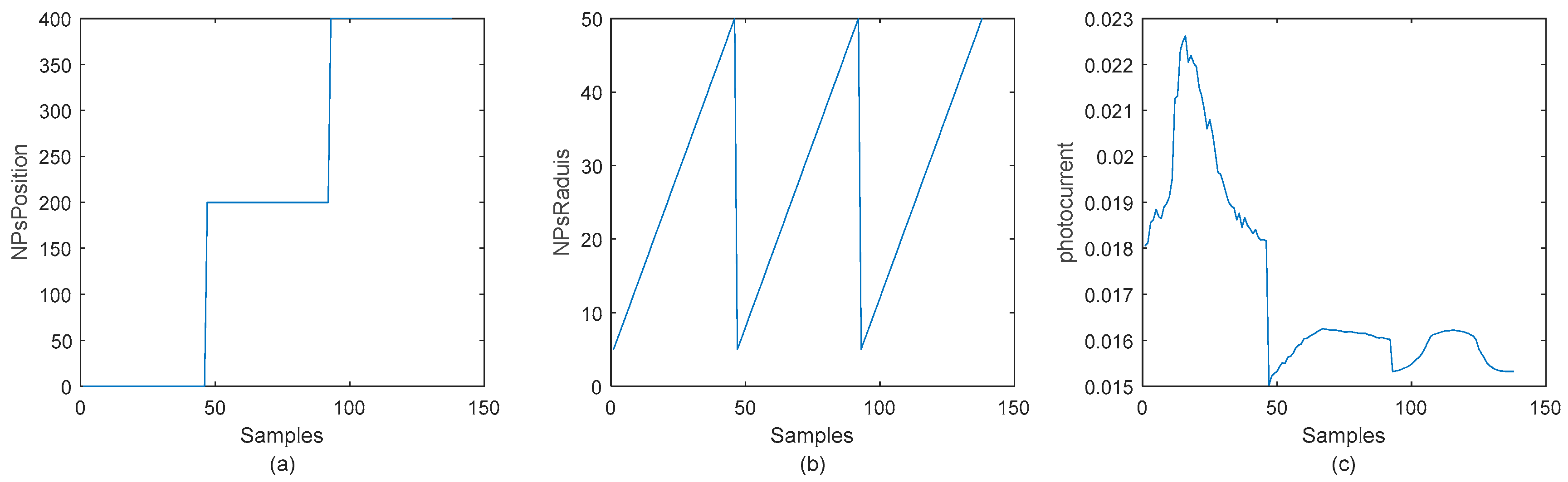
In the context of machine learning modeling, and since the collected data contain observations of 138 samples, which appears to be a light volume feature space, a simple data visualization method will be effective in providing guidance on both feature and model selection. Accordingly, Figure 3 deals with both inputs (Figure 3a,b) and outputs (Figure 3c) of the dataset. First, the photocurrent variation shows a kind of monotonicity in the deterioration by demonstrating a kind of regular degradation behavior over time. Similarly, such patterns can also be distinguished in the NPs’ positions. Whereas NPs’ radius exhibits a sort of periodicity that corresponds neither to inputs nor outputs. In this case, a first look at the feature selection strongly suggests eliminating these unnecessary features, which definitely lead to model bias. Second, variations in NPs’ positions and photocurrent over time show clear behavior of data drift. This means that this type of data are subject to continuous change in its characteristics, making the model generalization out-of-date, if one is not considering such an issue.
In this work, suggestions for overcoming these challenges are twofold. First, the data are subjected to a feature selection process including only NPs’ position features. After that, these features are also made subject to a normalization layer via min–max scaling in the range [0,1]. Second, adaptive learning rules are also integrated to ensure that the model is continually updated with new data and overcomes data drift issues. In this case, data drift problems are addressed by involving a neural network with long-short term memory (LSTM) as in [11,12]. It is worth mentioning that the network hyperparameters are manually tuned based on a simple error–trial basis, as in Table 1. Meanwhile, a threefold cross-validation technique is used to ensure the stability and generalizability of the model on the dataset.
The model is evaluated according to a robust criterion that includes different estimation error measures, namely root mean squared error (RMSE), root mean of squares (RMS), and mean absolute error (MAE). In addition, the learning model is also subject to another performance evaluation criterion represented by R2. Simply put, the three errors should approach “zero”, while the R2, should approach the value of one for a better model performance. It is worth mentioning that the application of these evaluation criteria was carried out based on a validation set for each learning fold. This guarantees both the approximation capacity and the generalizability of the learning models. Additionally, another comparative study between the proposed architect and an ordinary multilayer perceptron (MLP) is also conducted. The comparison conclusions obtained will be very effective in observing the benefits of adaptive learning. An important point to consider in such a case is that the MLP uses the same hyperparameters to ensure a fair comparison.
The obtained results are summarized in Table 2. The cross-validation results of the RMSE, MSE, and MAE show an extremely better stability of LSTM compared to an ordinary MLP. Additionally, the mean values and standard deviation also explain this important information. This performance gap explains the need to use adaptive learning, on the one hand, and also the importance of feature selection, on the other hand. Furthermore, the results obtained regarding R2 clearly prove the explainability and importance of the predictions obtained.
4. Conclusions
In this paper a new computation framework based on combined SCAPS numerical simulations and machine learning has been developed. The proposed approach can rapidly and accurately predict the photosensing ability of SnS-based sensors, including plasmonic effects and the impact of the gold nanoparticles’ position and size. Applying LSTM learning rules to such a data drift and complexity problem allows the learning model to be updated based on any changes in the data. This is explained by great performance in approximation metrics such as the RMSE, MSE, and MAE. Meanwhile, R2 clearly demonstrates the importance of the results from an expandability perspective. As for the prospects, this work will continue to explore such a tool for more complex and massive data, to reach more generalized conclusions in the context of data complexity and drift.
Author Contributions
Conceptualization, A.M., F.D., T.B. and H.F.; methodology, F.D.; validation, H.F., T.B. and F.D.; formal analysis, H.F., T.B. and F.D.; investigation, H.F., T.B. and F.D.; data curation, H.F., T.B. and F.D.; writing—original draft preparation, F.D. and T.B.; writing—review and editing, H.F., T.B. and F.D.; All authors have read and agreed to the published version of the manuscript.
Funding
This research received no external funding.
Institutional Review Board Statement
Not applicable.
Informed Consent Statement
Not applicable.
Data Availability Statement
Data are available in this manuscript.
Conflicts of Interest
The authors declare no conflicts of interest.
References
- Kawamura, F.; Song, Y.; Murata, H.; Tampo, H.; Nagai, T.; Koida, T.; Imura, M.; Yamada, N. Tunability of the bandgap of SnS by variation of the cell volume by alloying with A.E. elements. Sci. Rep. 2022, 12, 7434. [Google Scholar] [CrossRef] [PubMed]
- Zhang, H.; Li, H.; Yu, H.; Wang, F.; Song, X.; Xu, Z.; Wei, D.; Zhang, J.; Dai, Z.; Ren, Y.; et al. High responsivity and broadband photodetector based on SnS2/Ag2S heterojunction. Mater. Lett. 2023, 330, 133037. [Google Scholar] [CrossRef]
- Dong, W.; Lu, C.; Luo, M.; Liu, Y.; Han, T.; Ge, Y.; Xue, X.; Zhou, Y.; Xu, X. Enhanced UV–Vis photodetector performance by optimizing interfacial charge transportation in the heterostructure by SnS and SnSe2. J. Colloid Interface Sci. 2022, 621, 374–384. [Google Scholar] [CrossRef] [PubMed]
- Ye, Z.; Yu, H.; Wei, J.; Xie, Y. Direct observation of kinetic characteristic on SnS-based self-powered photodetection. J. Lumin 2023, 253, 119473. [Google Scholar] [CrossRef]
- Kacha, K.; Djeffal, F.; Ferhati, H.; Foughali, L.; Bendjerad, A.; Benhaya, A.; Saidi, A. Efficiency improvement of CIGS solar cells using RF sputtered TCO/Ag/TCO thin-film as prospective buffer layer. Ceram. Int. 2022, 48, 20194–20200. [Google Scholar] [CrossRef]
- Trukhanov, S.V.; Bodnar, I.V.; Zhafar, M.A. Magnetic and electrical properties of (FeIn2S4)1−x(CuIn5S8)x solid solutions. J. Magn. Magn. Mater. 2015, 379, 22–27. [Google Scholar] [CrossRef]
- Bodnar, I.V.; Jaafar, M.A.; Pauliukavets, S.A.; Trukhanov, S.V.; Victorov, I.A. Growth, optical, magnetic and electrical properties of CuFe2.33In9.67S17.33 single crystal. Mater. Res. Express 2015, 2, 085901. [Google Scholar] [CrossRef]
- Zdorovets, M.V.; Kozlovskiy, A.L.; Shlimas, D.I.; Borgekov, D.B. Phase transformations in FeCo—Fe2CoO4/Co3O4-spinel nanostructures as a result of thermal annealing and their practical application. J. Mater. Sci. Mater. Electron. 2021, 32, 16694–16705. [Google Scholar] [CrossRef]
- Migas, D.B.; Turchenko, V.A.; Rutkauskas, A.V.; Trukhanov, S.V.; Zubar, T.I.; Tishkevich, D.I.; Trukhanov, A.V.; Skorodumova, N.V. Temperature induced structural and polarization features in BaFe12O19. J. Mater. Chem. C 2023, 11, 12406–12414. [Google Scholar] [CrossRef]
- Troyanchuk, I.O.; Trukhanov, S.V.; Szymczak, H.; Baerner, K. Effect of oxygen content on the magnetic and transport properties of Pr0.5Ba0.5MnO3-γ. J. Phys. Condens. Matter. 2000, 12, L155–L158. [Google Scholar] [CrossRef]
- Kozlovskiy, A.; Egizbek, K.; Zdorovets, M.V.; Ibragimova, M.; Shumskaya, A.; Rogachev, A.A.; Ignatovich, Z.V.; Kadyrzhanov, K. Evaluation of the efficiency of detection and capture of manganese in aqueous solutions of FeCeOx nanocomposites doped with Nb2O5. Sensors 2020, 20, 4851. [Google Scholar] [CrossRef] [PubMed]
- Berghout, T.; Mouss, M.-D.; Mouss, L.-H.; Benbouzid, M. ProgNet: A Transferable Deep Network for Aircraft Engine Damage Propagation Prognosis under Real Flight Conditions. Aerospace 2022, 10, 10. [Google Scholar] [CrossRef]
Figure 1.
(a) Cross-sectional view of plasmonic gold nanoparticles based on the SnS absorber film (b) schematic of SnS surface, decorated with Au NPs.
Figure 1.
(a) Cross-sectional view of plasmonic gold nanoparticles based on the SnS absorber film (b) schematic of SnS surface, decorated with Au NPs.

Figure 2.
Variation of the photocurrent as a function of the Au NPs’ radius.
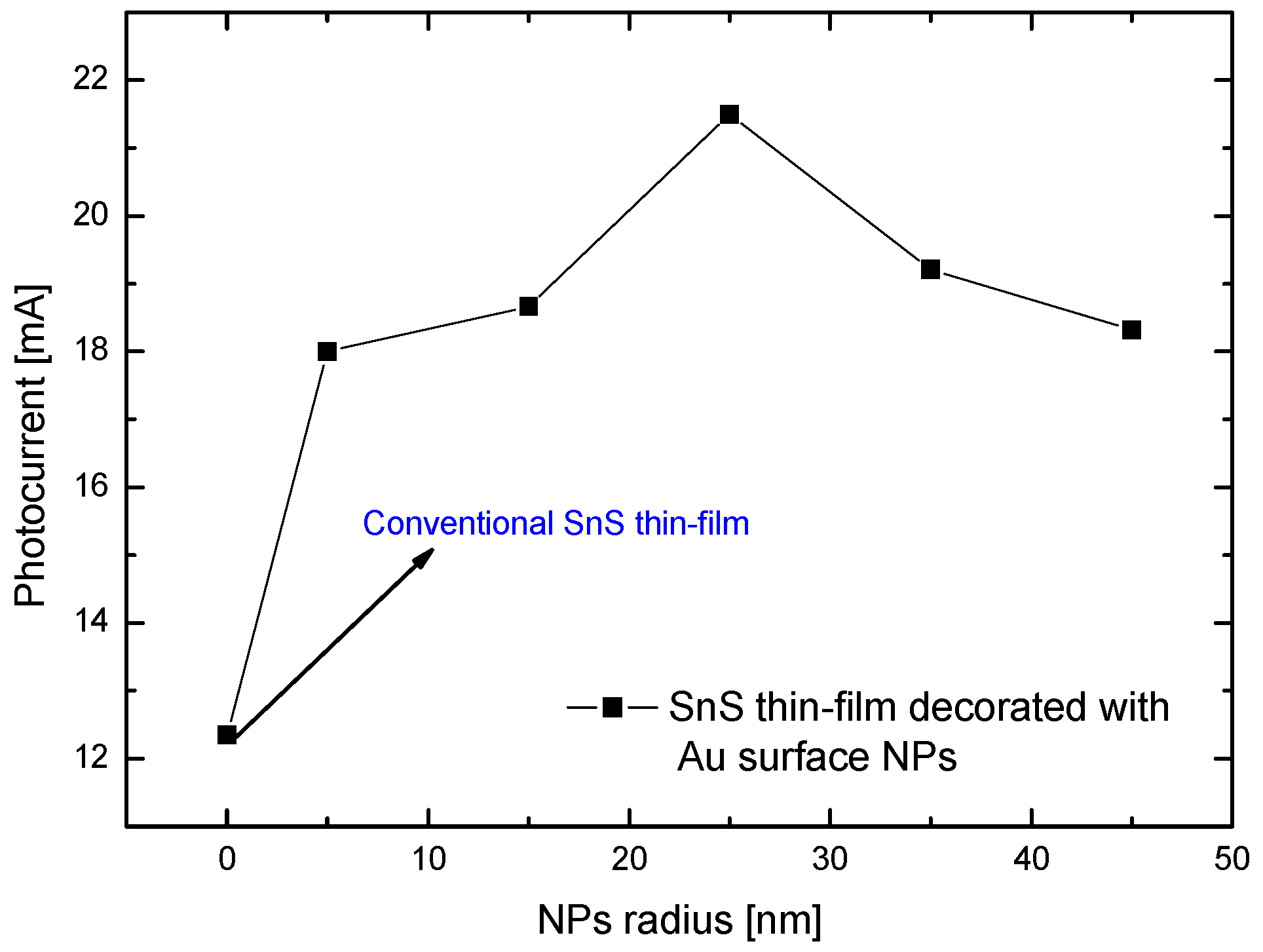
Figure 3.
Dataset features: (a,b) inputs; (c) output.

Table 1.
List of obtained hyperparameters.
| Hyperparameters | Assigned Values |
|---|---|
| Maximum number of epochs | 300 |
| Mini batch size | 30 |
| Neurons | 20 |
| Learning algorithm | Adam optimizer |
| Initial learning rate | 0.01 |
| Gradient threshold | 1 |
| L2 regularization | 0.0001 |
Table 2.
Performance evaluation results.
| LSTM | ||||
|---|---|---|---|---|
| Cross-validation Folds | RMSE | MSE | MAE | R2 |
| 1 | 9.49 × 10⁻⁴ | 9.00 × 10⁻⁷ | 6.85 × 10⁻⁴ | 0.72 |
| 2 | 1.03 × 10⁻³ | 1.07 × 10⁻⁶ | 7.10 × 10⁻⁴ | 0.75 |
| 3 | 1.25 × 10⁻³ | 1.56 × 10⁻⁶ | 9.16 × 10⁻⁴ | 0.65 |
| Average | 1.07 × 10⁻³ | 1.18 × 10⁻⁶ | 7.7 × 10⁻⁴ | 0.71 |
| Standard deviation | 4.91 × 10⁻⁴ | 0.051 | ||
| MLP | ||||
| Cross-validation folds | RMSE | MSE | MAE | R2 |
| 1 | 2.09 × 10⁻³ | 4.40 × 10⁻⁶ | 1.63 × 10⁻³ | −0.36 |
| 2 | 1.65 × 10⁻³ | 2.74 × 10⁻⁶ | 1.31 × 10⁻³ | 0.382 |
| 3 | 1.37 × 10⁻³ | 1.89 × 10⁻⁶ | 1.12 × 10⁻³ | 0.58 |
| Average | 1.71 × 10⁻³ | 3.01 × 10⁻⁶ | 1.35 × 10⁻³ | 0.20 |
| Standard deviation | 8.11 × 10⁻⁴ | 0.5003 | ||
Disclaimer/Publisher’s Note: The statements, opinions and data contained in all publications are solely those of the individual author(s) and contributor(s) and not of MDPI and/or the editor(s). MDPI and/or the editor(s) disclaim responsibility for any injury to people or property resulting from any ideas, methods, instructions or products referred to in the content. |
© 2023 by the authors. Licensee MDPI, Basel, Switzerland. This article is an open access article distributed under the terms and conditions of the Creative Commons Attribution (CC BY) license (https://creativecommons.org/licenses/by/4.0/).
Share and Cite
MDPI and ACS Style
Maoucha, A.; Djeffal, F.; Berghout, T.; Ferhati, H. Photoresponsivity Enhancement of SnS-Based Devices Using Machine Learning and SCAPS Simulations. Eng. Proc. 2023, 58, 128. https://doi.org/10.3390/ecsa-10-16014
AMA Style
Maoucha A, Djeffal F, Berghout T, Ferhati H. Photoresponsivity Enhancement of SnS-Based Devices Using Machine Learning and SCAPS Simulations. Engineering Proceedings. 2023; 58(1):128. https://doi.org/10.3390/ecsa-10-16014
Chicago/Turabian StyleMaoucha, Abdelhak, Faycal Djeffal, Tarek Berghout, and Hichem Ferhati. 2023. "Photoresponsivity Enhancement of SnS-Based Devices Using Machine Learning and SCAPS Simulations" Engineering Proceedings 58, no. 1: 128. https://doi.org/10.3390/ecsa-10-16014