Abstract
In this paper, we present a RISC-V RV32I-based system-on-chip (SoC) design approach using the Vivado high-level synthesis (HLS) tool. The proposed approach consists of three separate levels: The first one is an HLS design and simulation purely in C++. The second one is a Verilog simulation of the HLS-generated Verilog implementation of the CPU core, a RAM unit initialized with a short assembly code, and a simple output port which simply forwards the output data to the simulation console. Finally, the third level is the implementation and testing of this SoC on a low-cost FPGA board (Basys3) running at a clock speed of 100 MHz. A sample C code was compiled using the GNU RISC-V compiler tool chain and tested on the HLS-generated RISC-V RV32I core as well. The HLS design consists of a single C++ file with fewer than 300 lines, a single header file, and a testbench in C++. Our design objectives are that (1) the C++ code should be easy to read for an average engineer, and (2) the coding style should dictate minimal area, i.e., minimal resource utilization, without significantly degrading the code readability. The proposed system was implemented for two different I/O bus alternatives: (1) a traditional single clock cycle delay memory interface and (2) the industry-standard AXI bus. We present timing closure, resource utilization, and power consumption estimates. Furthermore, by using the open-source synthesis tool yosys, we generated a CMOS gate-level design and provide gate count details. All design, simulation, and constraint files are publicly available in a GitHub repo. We also present a simple dual-core SoC design, but detailed multi-core designs and other advanced futures are planned for future research.
1. Introduction
In this paper, we present a RISC-V RV32I-based system-on-chip (SoC) design and implementation using a high-level synthesis (HLS) approach. The complete core design was carried out with HLS and then simulated at the C level, then at the Verilog level, and finally tested on a low-cost FPGA board at 100 MHz clock speed. Both assembly programs and C programs compiled with the GNU RISC-V toolchain were used as RAM images for testing the HLS-generated core. The proposed HLS core design has a single C++ file with fewer than 300 lines and is designed to be both highly-readable and use minimal hardware resources.
There are several published papers for CPU design in different hardware description languages (HDLs). In [1], a very simple reduced instruction set (RISC) processor design is presented with about 120 lines of Verilog code. See [2,3,4] and references therein for related work. RISC-V is a free and open source instruction set architecture [5,6]. The standard defines various ISAs starting with the base architecture RV32I. There are numerous Verilog implementations of RISC-V architectures, with varying degrees of performance and resource utilization. The paper [7] presents a review of some of the well-known open source designs and links to relevant GitHub repos for source codes. One disadvantage of these Verilog implementations is the length of the source codes, which is the main motivation for the HLS-based approach adapted in this work. The HLS-based approach can be quite useful for rapid prototyping of complex ideas, especially for systems with complex state machines. To the best of author’s knowledge, there is limited published work where an HLS-based approach is used for a RISC-V core design. In [8], an HLS design is presented, but the source code is split into multiple files, making it difficult to read. This work presents a single file design which is relatively short, easily readable, and yet suitable for an FPGA implementation with clock speeds of 100 MHz. Open source RISC-V cores can be quite useful for computer architecture education too; see [9]. The proposed HLS RISC-V RV32I core source codes are available in the public GitHub repo [10]. Finally, the author would like to cite [11] as a source of inspiration for this work.
This paper is organized as follows: In Section 2, we summarize the RISC-V RV32I instruction set architecture. In Section 3, a high-level synthesis approach for design and simulation is presented. Verilog simulations of our RISC-V SoC are presented in Section 4, CMOS gate-level design using the open-source synthesis tool yosys and gate count details are given in Section 5, and the FPGA implementation and testing are presented in Section 6. A sample C program was used for testing the HLS-generated core, as outlined in Section 7. A multi-core RISC-V SoC approach is outlined in Section 8, and finally some concluding remarks are given in Section 9.
2. RISC-V RV32I Architecture
In this section, we summarize the RISC-V RV32I instruction set architecture (ISA) [5,6] in Table 1. From a programming perspective, there are 32 registers x0,⋯,x31 and a program counter PC, all having 32-bit size. The register x0 is hardwired to 0, and the instructions are divided into six different groups R (Register), I (Immediate), S (Store), B (Branch), J (Jump), and U (Upper) [5,6]. Full details of the instruction encoding and instruction fields are given in [5,6]. For the HLS implementation of the instruction decoder stage, we divide type instructions into IA (Immediate arithmetic), IM (Immediate memory), IJ (Immediate jump), and IE (Immediate exception) groups. Furthermore, type instructions are divided into U1 (Upper1) and U2 (Upper2). All of the instructions are 32 bits in size and have a 7-bit opcode field located between bits 6 down to 0. Furthermore, there are 3-bit func3, 7-bit func7, and imm fields, but not all instructions have all of these three additional fields [5,6].

Table 1.
RV32I instructions [5,6].
The sra and srai instructions use the most significant bit (MSB) extension rule, whereas the instructions sltu,sltiu,lbu,lhu,bltu, and bgeu use the zero extension rule. The instructions ecall and ebreak are implemented as trap/halt. All unaligned memory accesses are also implemented as trap/halt.
3. HLS Approach for Design and Simulation
The HLS design consists of the C++ file riscv32i.cc and the header file riscv32i.h. There is also a C simulation testbench file riscv32i_tb.cc. In this section, we simply summarize the main design ideas. The full source code is available in our GitHub repo [10].
We start with the outline of the design file riscv32i.cc; see Outline I. This file has only the cpu() function, which has two pointer arguments. For C simulation, they have the usual semantics, but for hardware synthesis, the first one is interpreted as a single-port RAM, and the other is implemented as a 4-bit write-strobe signal. The local array reg_file[] is interpreted as a multi-port RAM for hardware synthesis, which will correspond to the internal register file. The HLS tool has a standard C compiler which works according to standard semantic rules for simulations, but for hardware synthesis semantic details are different and can be controlled by using the #pragma HLS directives. Full details are available in the Vivado HLS User Guide [12].
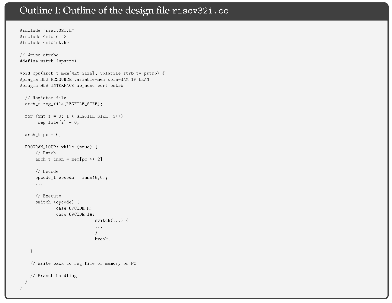
As seen in Outline I, immediately after resetting the program counter and all of the registers are initialized to zero, there is an infinite while loop which will be exited if an ECALL or EBREAK instruction is executed or an unaligned memory access is requested, basically causing the CPU core to halt.
The HLS tool converts this while loop to a state machine with 11 states using the one-hot encoding. Inside the loop, we have the usual instructions fetch, decode, execute, write-back, and branch handling. For example, insn = mem[pc >> 2] will be synthesized as a memory read operation, and opcode = insn(6,0) will be synthesized as selecting the least significant 7 bits of the 32-bit value read from the memory. Note that, by using the operator overloading features of C++, we are able to express slicing and concatenation in C++; see [10,12] for full details. For example, in the instruction decode stage, we have the lines
- immI = ( ((ap_int<ARCH>) insn) >> 20 );
- immS = ( immI(31,5), insn(11,8), insn(7,7) );
- immB = ...
- immJ = ...
- immU = ( insn(31,12), ((ap_uint<12>) 0) );
which correspond to generating the 32-bit immediate value for various types of instructions. Note that ap_uint<p> is used for p-bit unsigned integers, insn(p,q) corresponds to slicing, and ( … , … , … ) corresponds to concatenation. These are possible because of the standard operator loading features of C++. Note that the C simulation semantics and the hardware synthesis semantics are different.
There are various switch statements, which are synthesized as wide-multiplexers. Nested switch statements correspond to cascaded multiplexers. To make sure that minimal number of adders, comparators, barrel-shifters, etc., are synthesized, and no hardware resources are wasted or underutilized, we defined first program variables src1, src2, res and then wrote several switch statements. This coding style may appear slightly unusual but is still highly readable and is adapted purely for optimal hardware synthesis. In other words, the C++ coding style used in HLS greatly affects the final generated hardware, and we tried to keep a reasonable balance between C++ code readability and hardware optimality.
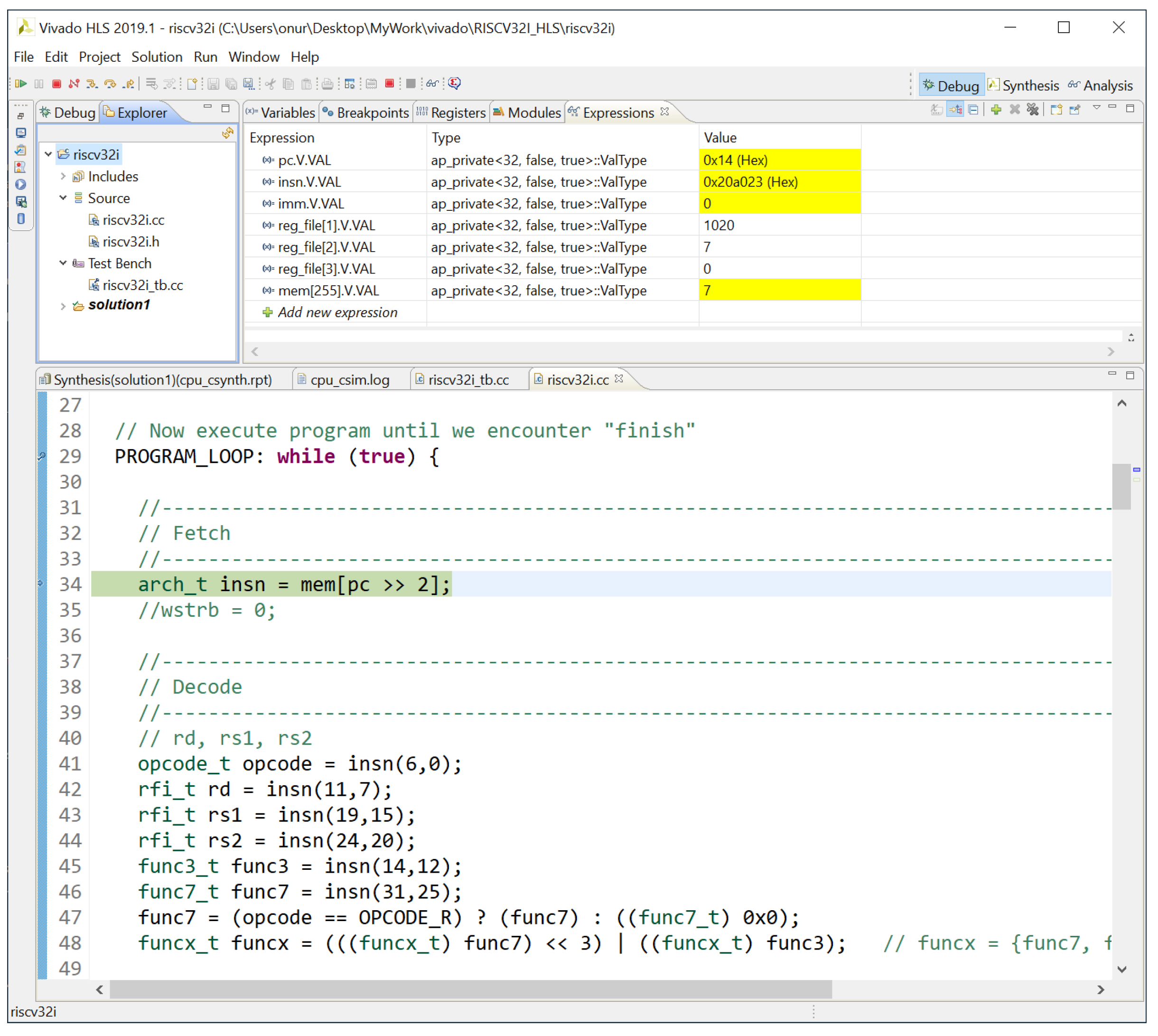
The HLS tool automatically generates Verilog files in a human-readable format but also allows C-simulation-based testing using the file riscv32i_tb.cc. This C-simulation testbench reads a text file of hexadecimal values in a human-readable format, initializes the memory by using these values, and passes the control to the cpu() function. Immediately after return, all register values and the memory are dumped to separate text files. In Figure 1, Vivado HLS C simulation for the following short assembly program is given:
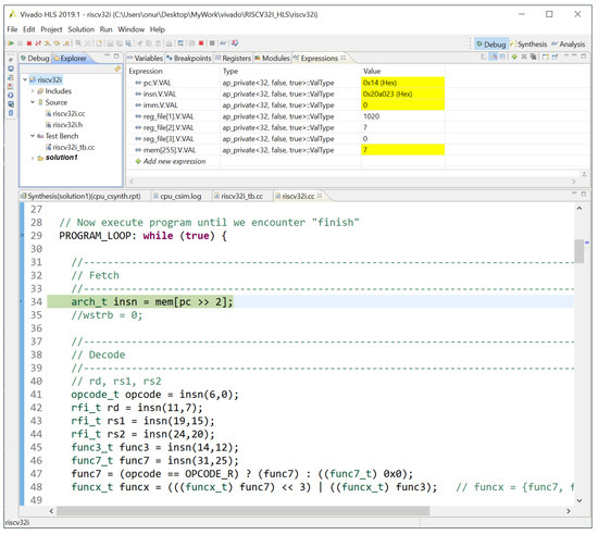
Figure 1.
Vivado HLS C simulation.
- li x1,1020
- sw x0,0(x1)
- loop: lw x2,0(x1)
- addi x2,x2,1
- sw x2,0(x1)
- j loop
Values stored in registers and memory as well as internal signals are displayed in the debug window. Hexadecimal values for each instruction are written to the file mem.txt, and conversion is carried out by using an online assembler tool. See [10] for full details.
4. RISC-V SoC Simulation in Verilog
In this section, we present Verilog simulation of the HLS-generated RISC-V core. Either one can copy the HLS-generated Verilog files to the Vivado project folder or create an IP object for a block-diagram-based design. We simply copy and paste the generated Verilog files from one folder to the other, but in the next FPGA-based design we will use the block-diagram-based design approach for better visualization of the overall system.
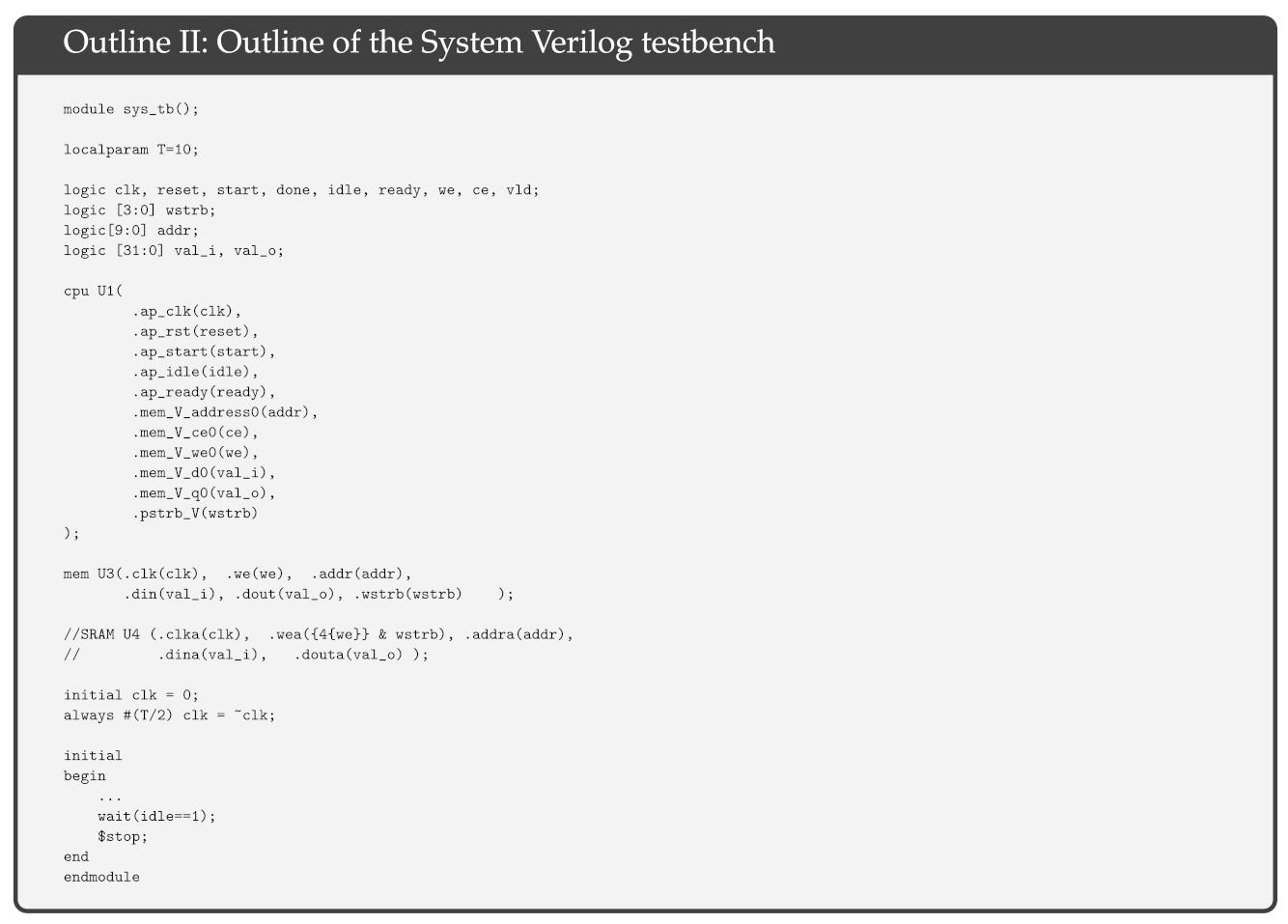
The simulation testbench outline is given in Outline II, and the RAM with the I/O devices is presented in Outline III. Basically, we have a simple system on chip consisting of a single RISC-V RV32I core, a 4 KB RAM with single clock cycle read/write delay, and a 32-bit output port at memory address 0x0ff.
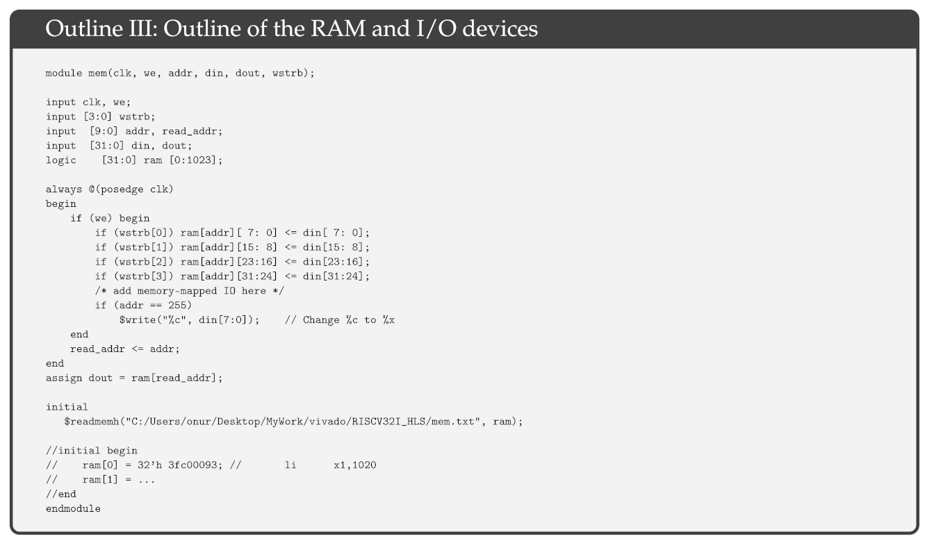
In Figure 2, Verilog simulation results are shown. We are using the assembly program given in the previous section, which basically writes the values 0, 1, 2, … to the address 0x0ff. The program counter PC is shown in the timing diagram, and the values written to the output port at address 0x0ff are shown both in the simulation console and the timing diagram. There is a specific reason why $write("%c", din[7:0]) is used for the memory mapped I/O at address 0x0ff. If we use a C-compiler and implement putc() as a write to the I/O address 0x0ff, then all printf(…) and cout << … will write to the Verilog simulation console. This allows more complex C/C++ programs to be tested with the HLS-generated RISC-V core.
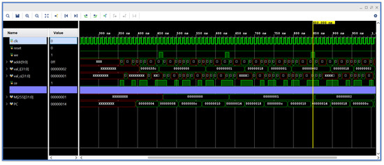
Figure 2.
Verilog simulation.
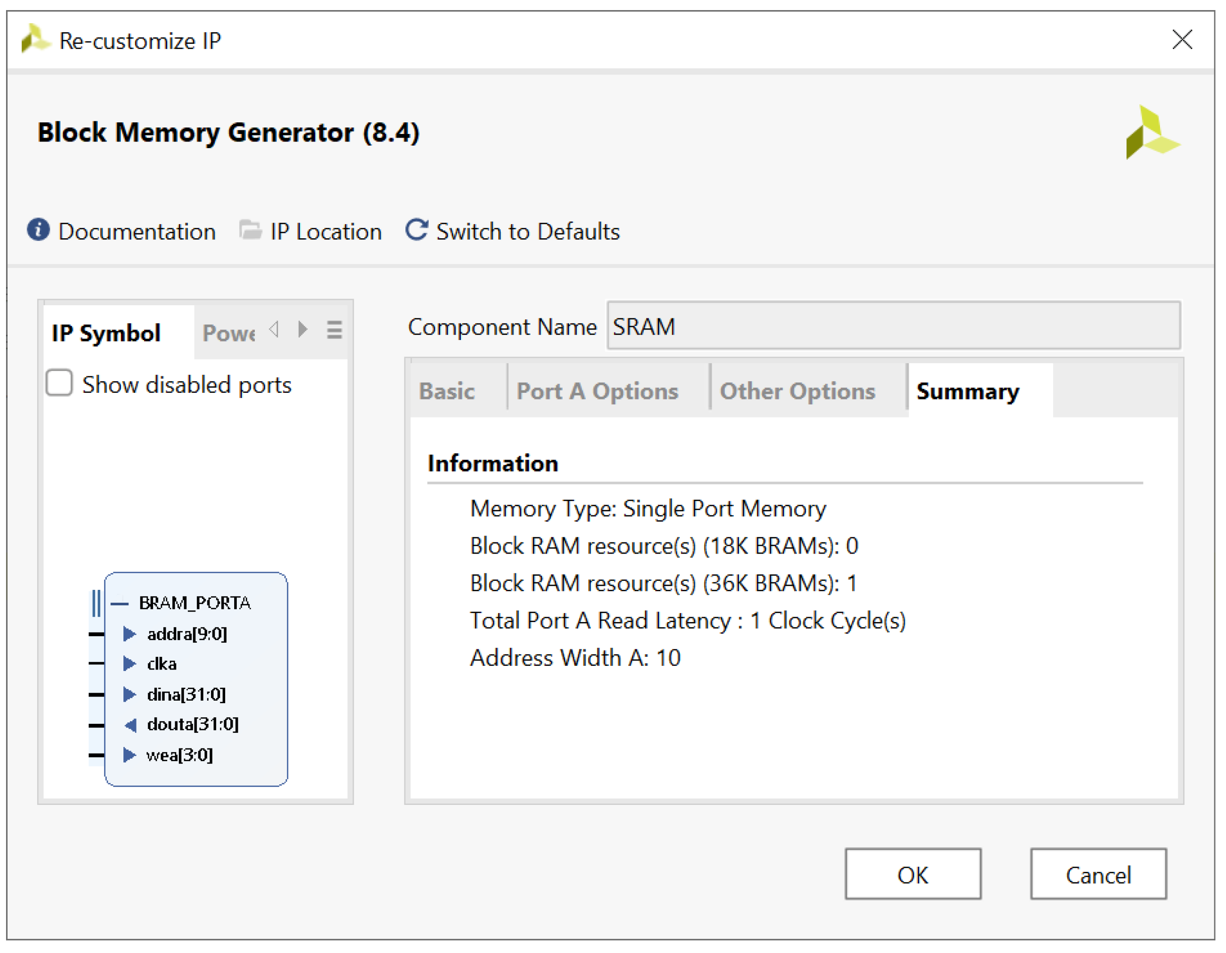
In our simulation testbench, we also have a block RAM option, shown as SRAM. This allows the HLS-generated RISC-V core to be tested using block RAMs available on most Xilinx FPGAs; see Figure 3.
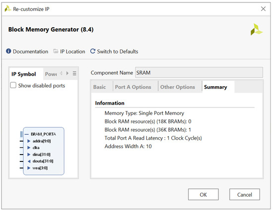
Figure 3.
Block RAM should have single clock cycle read/write delay.
5. RISC-V RV32I Core Synthesis Gate Counts
In this short section, we present gate count results for the CMOS gate-level design generated by the open-source synthesis tool yosys. The following script is for the synthesis tool
- read_verilog cpu.v cpu_reg_file_V.v
- hierarchy -check
- proc; opt; fsm; opt; memory; opt
- techmap; opt
- read_liberty -lib cmos_cells.lib
- abc -liberty cmos_cells.lib
- splitnets -ports; opt
- stat
and the following gate-count results are reported by the synthesis tool:
- === cpu ===
- Number of wires: 8282
- Number of cells:
- $_DFF_P_ 321
- NAND 2689
- NOR 3714
- NOT 924
- === cpu_reg_file_V ===
- Number of wires: 7714
- Number of cells:
- $_DFF_P_ 1056
- NAND 4726
- NOR 1505
- NOT 387
In summary, a total of 1377 D-type flip-flops are used, including the register file of depth 32 and width 32. We have forced the synthesis tool to design using only two input NAND and NOR gates, and with that constraint the total number of two-input NAND gates is 7415, two-input NOR gates is 5219, and NOT gates is 1311.
6. RISC-V SoC Implementation on an FPGA
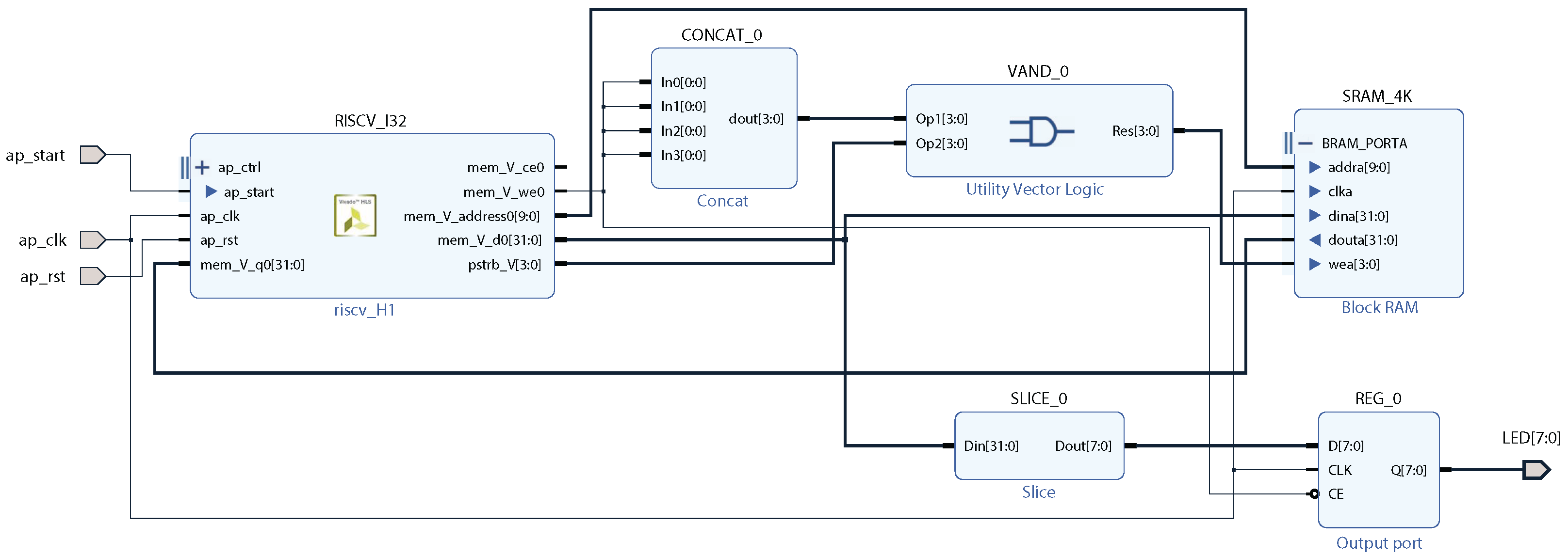
In this section, we will present a simple RISC-V SoC implemented on an FPGA. High-level details are presented in Figure 4, and the elaborated design is shown in Figure 5.
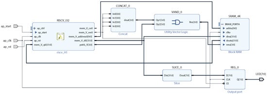
Figure 4.
A RISC-V SoC block diagram for FPGA implementation.
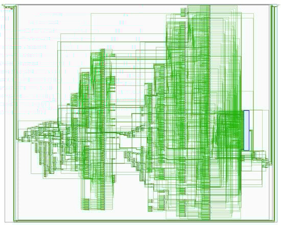
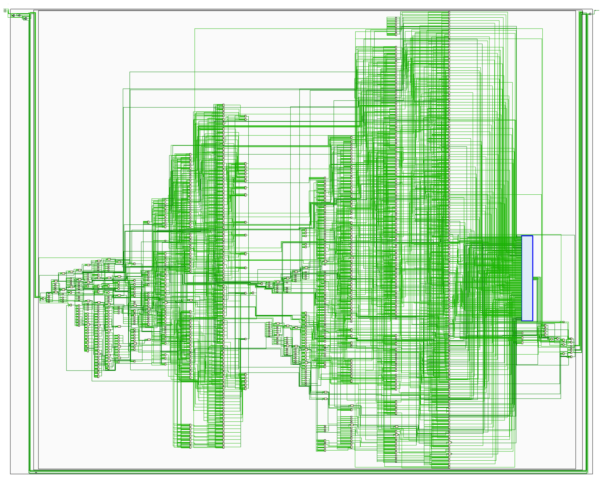
Figure 5.
Elaborated design of the RISC-V SoC. The blue box on the right corresponds to the register file.
The elaborated design has 1296 cells and 1968 nets.
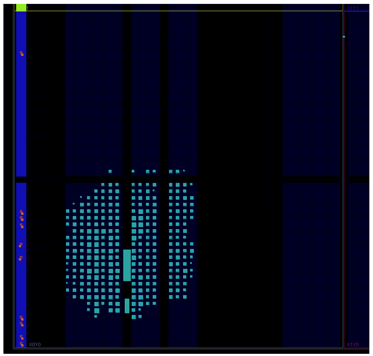
The resource utilization of the implemented design is 1078 LUT (5.18%), 326 FF (0.78%), and 3% of the BRAM. The final system has 1.41 ns worst-case negative slack for the setup time for 100 MHz clock. The power consumption is estimated as 81 mW at 100 MHz clock. Figure 6 shows the FPGA implementation of the SoC for the Basys3 board. Note that the whole SoC design fits into a portion of the clock region X0Y0. The large rectangular block at the center of Figure 6 is the 4 KB RAM used for the system on chip.
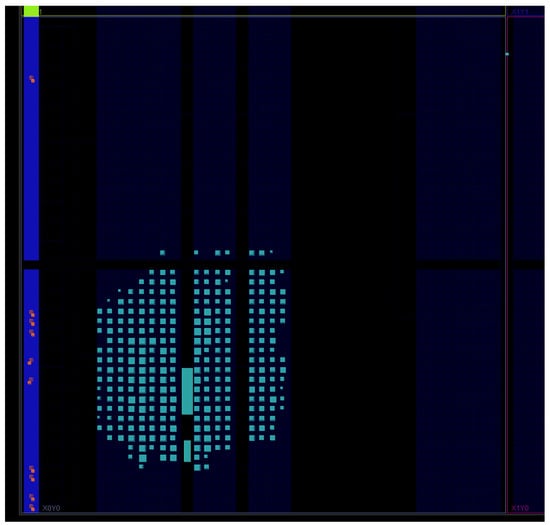
Figure 6.
RISC-V SoC FPGA implementation for the Basys3 board fits into a portion of the clock region X0Y0.
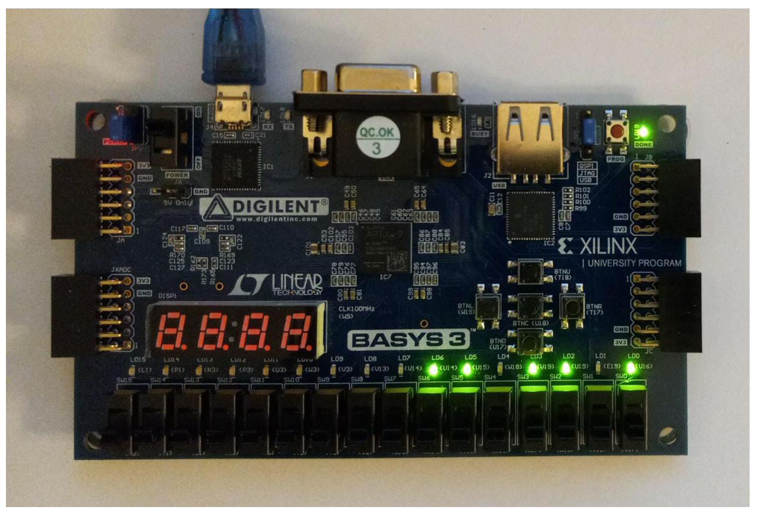
We use the same assembly program given in Section 3 and make sure that the hex values corresponding to assembly instructions are loaded to the SoC RAM. After the system is reset using the button btnC, the CPU core can be started using the button btnU. Figure 7 shows a Basys3 board implementation of our RISC-V SoC with the output port connected to the on-board LEDs. Note that bits 20 down-to 13 of the 32-bit value written to memory are routed to the I/O port using the slice block shown in Figure 4. The assembly program given in Section 3 has a loop execution time of 170 ns, i.e., 17 clock cycles loop execution time. The slicing block effectively slows down the counting speed so that counting can be observed by the naked eye.
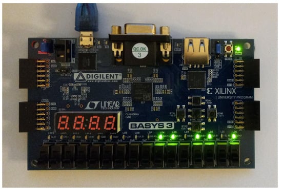
Figure 7.
RISC-V SoC implemented on a Basys3 board.
7. Testing with a Sample C Program
We used a short C program for simulating the RISC-V H1 core designed earlier. Our testcode is given below
- #define OUTPORT (0x0ff)
- #include <stdint.h>
- void main(void);
- void main(void) {
- *((volatile uint32_t*)OUTPORT) = ’R’;
- *((volatile uint32_t*)OUTPORT) = ’I’;
- *((volatile uint32_t*)OUTPORT) = ’S’;
- *((volatile uint32_t*)OUTPORT) = ’C’;
- *((volatile uint32_t*)OUTPORT) = ’\n’;
- }
It is compiled with the GNU RISC-V compiler to generate the RAM image. As shown in Outline III, we have a $readmemh to initialize the RAM for the Verilog simulation. Again as shown in the Outline III, all writes to address 0x0ff are forwarded to the simulation console using the $write command. In summary, when the SoC is simulated with the GNU RISC-V compiler to generate the RAM image, we see the string ‘RISC’ written to the console followed by a newline, which serves as another verification of the H1 core. In a future version of the paper, we will use longer C programs for more comprehensive testing.
8. A Multi-Core RISC-V SoC
In this section, we briefly summarize our multi-core RISC-V SoC implementation. We started by changing the memory interface from block RAM to a AXI master, i.e., changing the HLS directive to #pragma HLS INTERFACE m_axi depth=1024 port=mem. This resulted in a different RISC-V RV32I core equipped with the AXI master interface. The Vivado HLS generates a Verilog implementation with 42 states, which we call the H2 core. For this AXI-equipped H2 core, we need to delete the write-strobe port, wstrb, and use
- (mem[addr >> 2])( 7,0) = res;
- (mem[addr >> 2])(16,0) = res;
- (mem[addr >> 2])(32,0) = res;
to implement byte, word, and double-word sized memory write operations, respectively. Note that the bit-slicing operator (.,.) can be used both on the left- and right-hand side of expressions.
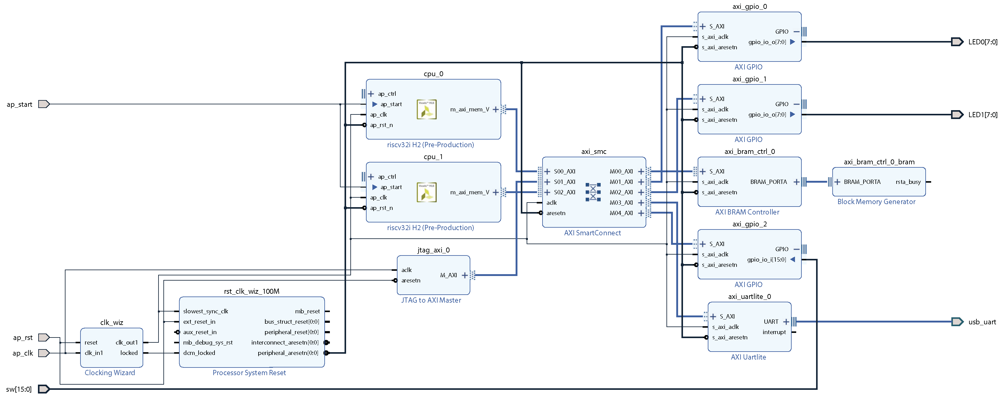
In Figure 8, we have a dual-core RISC-V RV32I system with 8K on-chip RAM, two 8-bit output ports, a 16-bit input port, and a single UART port. The H2 core does not have a tightly coupled memory (TCM) inside the unit, but this will be addressed in a future version of the paper. Basically, in the current implementation, both cores are using the on-chip static RAM over the AXI bus. All GPIOs and the UART unit are also on the AXI-bus. We have added a JTAG to AXI unit which can be used for debugging and initialization of the on-chip static RAM. For this dual-core SoC to function properly, both cores should have different reset vectors so that they can execute different programs independently.

Figure 8.
A dual-core RISC-V SoC for FPGA implementation.
Based on our preliminary results, we see that the dual-core RISC-V system shown in Figure 8 does fit into a Basys3 board.
9. Conclusions
In this paper, we have presented a high-level synthesis approach for RISC-V RV32I system design. The CPU core was designed and simulated at the C level, then the HLS-generated Verilog code was tested with RAM and I/O devices at the Verilog simulation level. Finally, the complete system-on-chip design with memory and I/O devices was implemented and tested on a low-cost FPGA board. Timing closure, resource utilization, and power consumption estimates are presented. The CMOS gate-level design and gate counts were generated by using an open-source synthesis tool. We have also outlined a dual-core system design. The HLS-generated CPU core has 14 states for a traditional single clock cycle delay memory interface and 42 states if the AXI bus support is needed. For such more complex systems, design in Verilog will be more demanding and error-prone compared to an HLS-based approach. Detailed analysis of multi-core designs are planned for future research.
Funding
Funding is provided by NSF-1919855, Advanced Mobility Institute grants GR-2000028, GR-2000029, and Florida Polytechnic University startup grant GR-1900022.
Institutional Review Board Statement
Not applicable.
Informed Consent Statement
Not applicable.
Data Availability Statement
Not applicable.
Acknowledgments
The author would like to acknowledge the support from NSF-1919855, Florida Polytechnic University, and AMI.
Conflicts of Interest
The author declares no conflicts of interest.
References
- Depablo, S.; Cebrián, J.A.; Herrero-de Lucas, L.C.; Rey-Boué, A.B. A very simple 8-bit RISC processor for FPGA. In Proceedings of the FPGAworld Conference 2006, Stocholm, Sweden, November 2006; pp. 9–15. [Google Scholar]
- Archana, H.R.; Sanjana, T.; Bhavana, H.T.; Sunil, S.V. System Verification and Analysis of ALU for RISC Processor. In Proceedings of the 2021 7th International Conference on Advanced Computing and Communication Systems (ICACCS), Coimbatore, India, 19–20 March 2021; Volume 1, pp. 1785–1789. [Google Scholar] [CrossRef]
- Wang, L.; Yu, Z.; Zhang, D.; Qin, G. Research on Multi-Cycle CPU Design Method of Computer Organization Principle Experiment. In Proceedings of the 2018 13th International Conference on Computer Science Education (ICCSE), Colombo, Sri Lanka, 8–11 August 2018; pp. 1–6. [Google Scholar] [CrossRef]
- Eljhani, M.M.; Kepuska, V.Z. Reduced Instruction Set Computer Design on FPGA. In Proceedings of the 2021 IEEE 1st International Maghreb Meeting of the Conference on Sciences and Techniques of Automatic Control and Computer Engineering MI-STA, Tripoli, Libya, 25–27 May 2021; pp. 316–321. [Google Scholar] [CrossRef]
- Waterman, A.; Asanović, K. The RISC-V Instruction Set Manual, Volume I: Unprivileged ISA Version 20191213; RISC-V International: San Francisco, CA, USA, 2021. [Google Scholar]
- RV32I Base Integer Instruction Set, Version 2.1. Available online: https://five-embeddev.com/riscv-isa-manual/latest/rv32.html (accessed on 14 November 2023).
- Höller, R.; Haselberger, D.; Ballek, D.; Rössler, P.; Krapfenbauer, M.; Linauer, M. Open-Source RISC-V Processor IP Cores for FPGAs — Overview and Evaluation. In Proceedings of the 2019 8th Mediterranean Conference on Embedded Computing (MECO), Budva, Montenegro, 10–14 June 2019; pp. 1–6. [Google Scholar] [CrossRef]
- Rokicki, S.; Pala, D.; Paturel, J.; Sentieys, O. What You Simulate Is What You Synthesize: Design of a RISC-V Core from C++ Specifications. In Proceedings of the RISC-V Workshop 2019, Zurich, Switzerland, June 2019; pp. 1–2. [Google Scholar]
- Harris, S.L.; Chaver, D.; Piñuel, L.; Gomez-Perez, J.; Liaqat, M.H.; Kakakhel, Z.L.; Kindgren, O.; Owen, R. RVfpga: Using a RISC-V Core Targeted to an FPGA in Computer Architecture Education. In Proceedings of the 2021 31st International Conference on Field-Programmable Logic and Applications (FPL), Dresden, Germany, 30 August–3 September 2021; pp. 145–150. [Google Scholar] [CrossRef]
- Toker, O. GitHub Repo for RISC-V RV32I HLS CPU Core H1. 2021. Available online: https://github.com/onurtoker/hls_riscv (accessed on 14 November 2023).
- Moreau, T. CPU Design in HLS. 2018. Available online: https://gitlab.cs.washington.edu/cse599s/hls-tutorials/-/tree/master/part3 (accessed on 14 November 2023).
- Vivado Design Suite User Guide, High-Level Synthesis. 2019. Available online: https://www.xilinx.com/support/documentation/sw_manuals/xilinx2019_1/ug902-vivado-high-level-synthesis.pdf (accessed on 14 November 2023).

Disclaimer/Publisher’s Note: The statements, opinions and data contained in all publications are solely those of the individual author(s) and contributor(s) and not of MDPI and/or the editor(s). MDPI and/or the editor(s) disclaim responsibility for any injury to people or property resulting from any ideas, methods, instructions or products referred to in the content. |
© 2023 by the author. Licensee MDPI, Basel, Switzerland. This article is an open access article distributed under the terms and conditions of the Creative Commons Attribution (CC BY) license (https://creativecommons.org/licenses/by/4.0/).