

Novel Current-Fed Bidirectional DC-DC Converter for Battery Charging in Electric Vehicle Applications with Reduced Spikes

 , and
, and 
Abstract
:1. Introduction
- Model current-fed bidirectional DC-DC converter with fewer switches in the EV charging application.
- Enhance the switching pulse generation using the FOPR controller-based pulse width modulation technique.
- Evaluate the converter topology under ZVS and ZCS operating conditions.
2. Related Works
3. Proposed Methodology
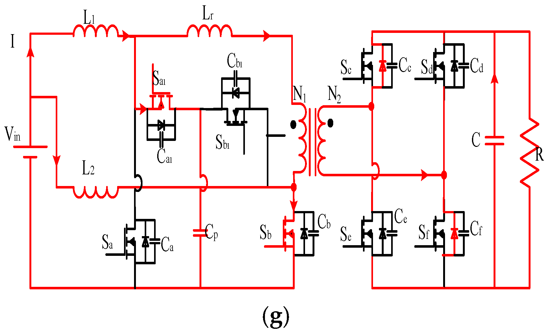
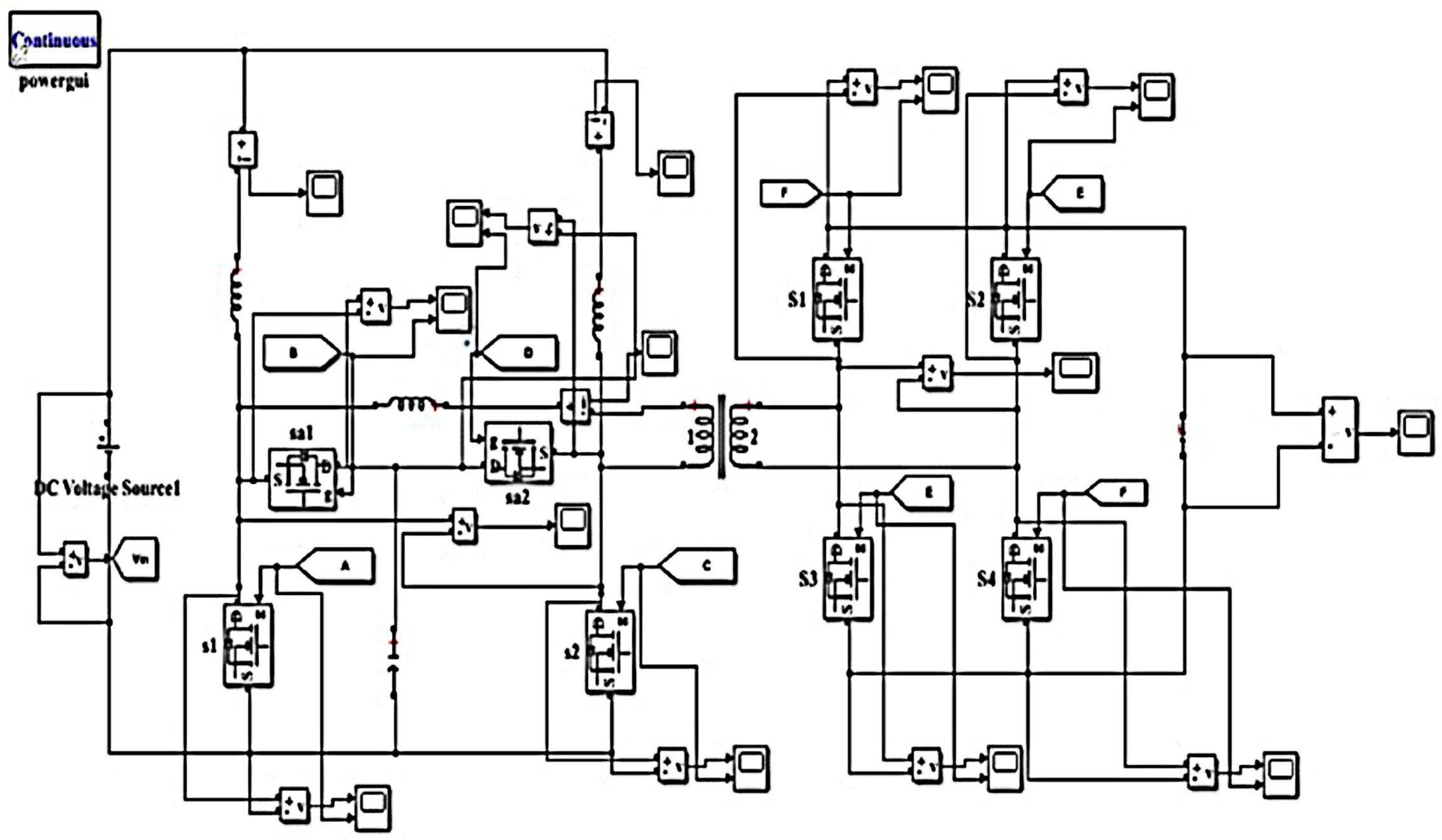
3.1. Proposed Current-Fed Isolated Bidirectional DC/DC Converter
3.2. Modes of Operation
- ➢
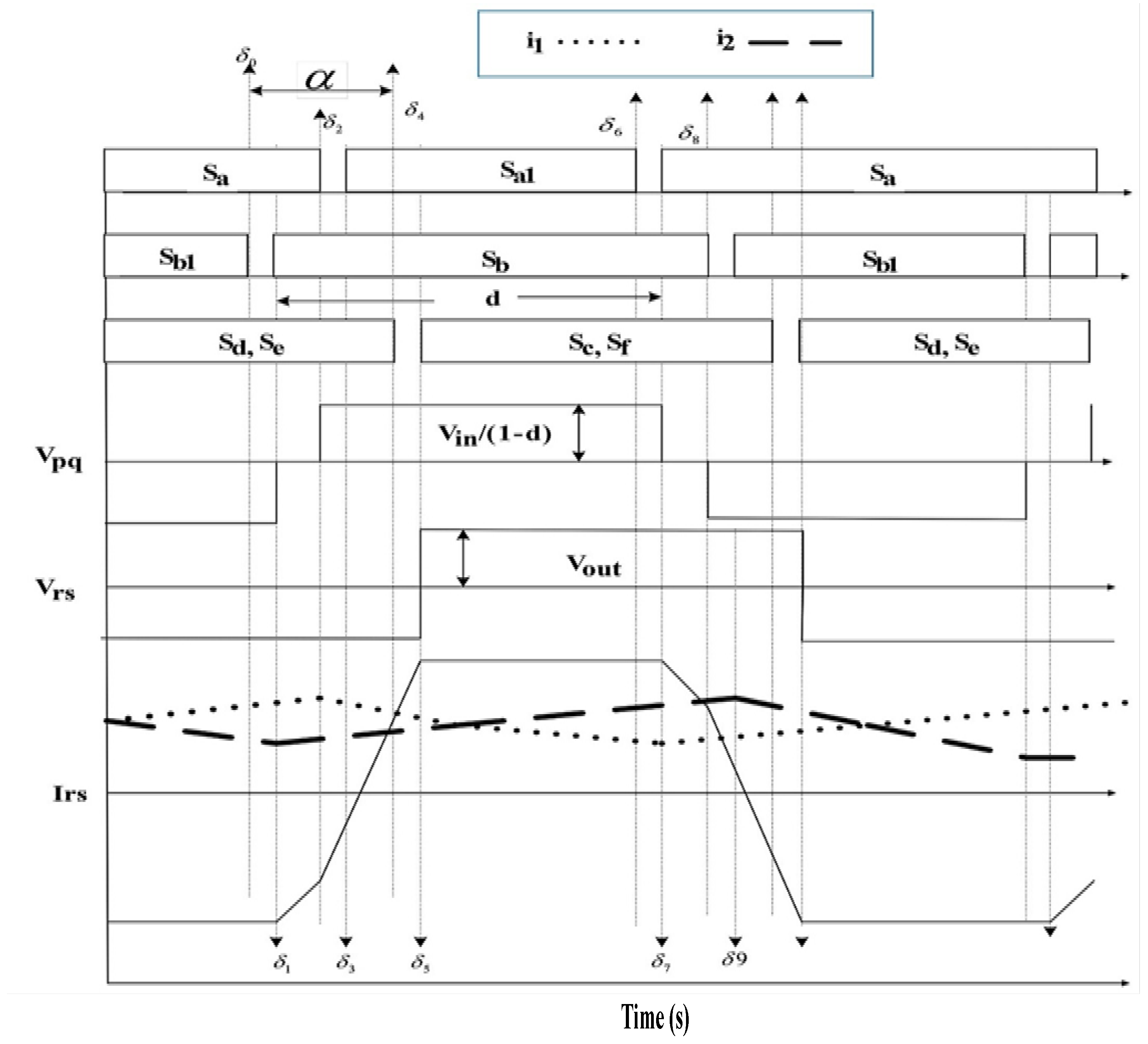
- Mode 0: In this mode, the switches Sa and Sb1 are closed on the primary side, and the switches Sd and Se are closed on the rectifying side or the secondary side converter. The inductor L1 stores energy by the switch Sa, and power is transferred from input to output. The current flow through the circuit in mode 0 is depicted in Figure 4a. The equation mentioned below gives the current flowing through the transformer or leakage inductance in this mode.where f is the switching frequency, ω is the angular frequency, Xlr is the leakage reactance of the transformer, Lr is the leakage inductance, ilr is the current flow through the transformer, and Vpq is the voltage between points p and q.
- ➢
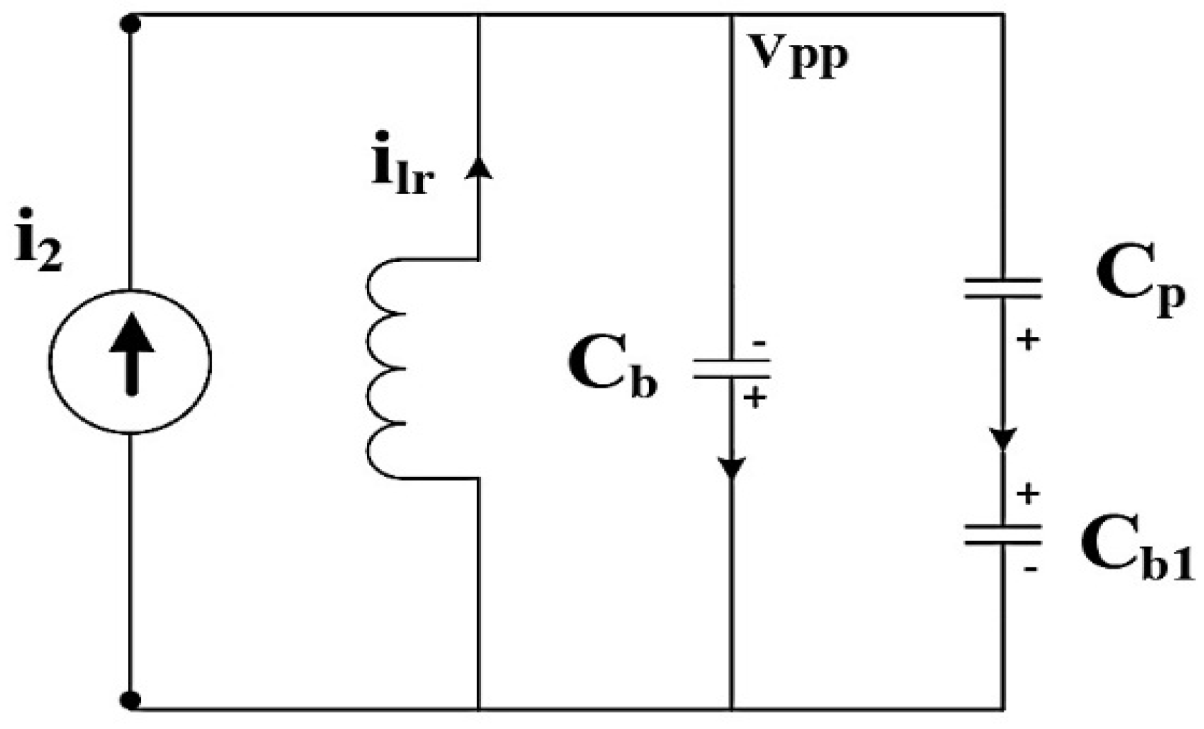
- Mode 1 (δ0 − δ1): In this mode, at δ0, the switch Sb1 is turned off, and switches Sa in the primary side and Sd and Se in the secondary side are closed. At the instant that Sb1 is turned off, Lr, Cb, and Cb1 begin to resonate, eliminating the voltage spikes at the switch Sb1 during turn-off. In the resonance, the condition Cb discharges the energy, and Cb1 charges. The current flowing through the circuit during mode 1 operation is shown in Figure 4b.
- ➢
- Mode 2 (δ1 − δ2): Cb is discharged fully, and therefore, Db starts conducting. Since Db is conducting, the voltage across the switch Sb is zero to obtain the ZVS. From the instant of δ1, the switch Sb can be turned on in the ZVS condition that is mathematically framed in the following equations. In this mode, Sa is conducted on the primary side, and Sb and Se are closed on the secondary side. δ1 − δ2 is the extra duration in which the main switch conducts for more than 0.5 d (d is the duty cycle). This extra duration is expressed below in terms of the duty cycle.Here, δ signifies the time duration, and N1 and N2 are the number of windings in the primary and secondary sides of the transformer. Current in the transformer primary during this mode is expressed in Equation (9). Vout is the voltage fed at the load, the same as the transformer’s secondary side voltage. The current flowing direction during mode 2 is shown in Figure 4c.
- ➢
- Mode 3 (δ2 − δ3): In this mode, at δ2, the switch Sa is turned off, and the switches Sb in the primary side and Sd and Se in the secondary side are closed. At the instant Sa is turned off, Lr, Ca, and Ca1 begin to resonate, eliminating the voltage spikes at the switch Sa during turn-off. In the resonance, the condition Ca1 discharges the energy, and Ca will charge. The current flowing through the transformer during this mode is derived as follows.
- ➢
- Mode 4 (δ3 − δ4): In this mode, Ca1 is discharged fully, and therefore, Da1 starts conducting. Since Da1 is closed, the voltage across the switch Sa1 is zero. From the instant of δ3, the switch Sa1 can be turned on in the ZVS condition. The current through the leakage inductance reverses to a positive direction in the middle of this mode. In this mode, Sb is conducted on the primary side, and Sd and Se are conducted on the secondary side, but both are turned off δ4. The current flowing direction of mode 4 is shown in Figure 4e.
- ➢
- Mode 5 (δ4 − δ5): In this mode of operation, switches Se and Sd are turned off on the secondary side. On the primary side, Sb and Sa1 are already in conduction. During this mode, Lr, Cc, Cd, Ce, and Cf begin to oscillate. The capacitors of just turned-off switches charge (Cd and Ce), and the other two capacitors (CV and Cf) discharge through the leakage inductance of the transformer. The current flowing direction of mode 5 is shown in Figure 4f.
- ➢
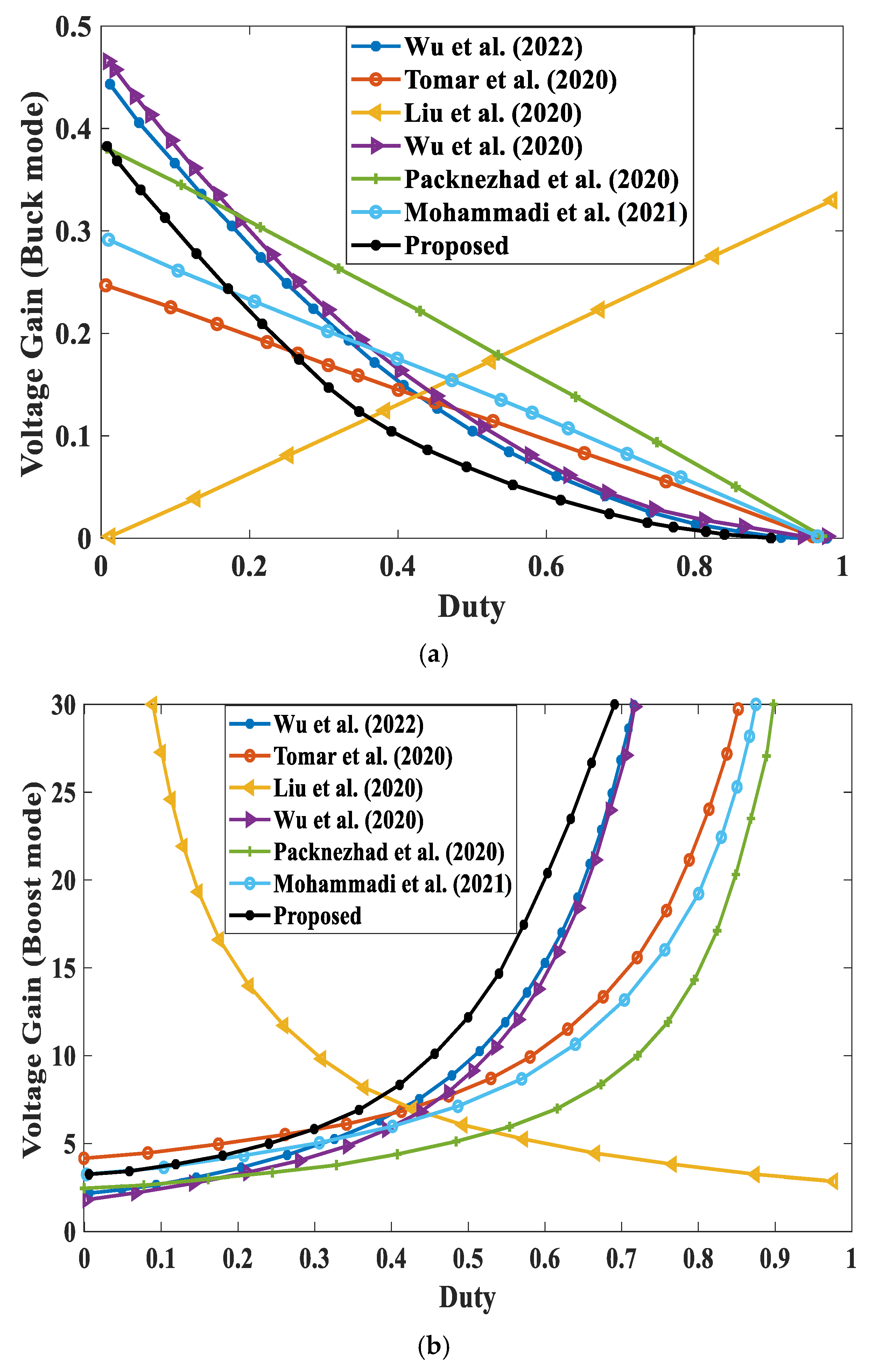
3.3. Voltage Matching by Varying Duty Cycle
3.4. Power Transfer by Phase Shift (α)
3.5. ZVS Condition
- Condition 1where β is (dTs)/8, Ts is the time period of switching frequency, and d is the duty cycle of the main switches.
- Condition 2
- Condition 3
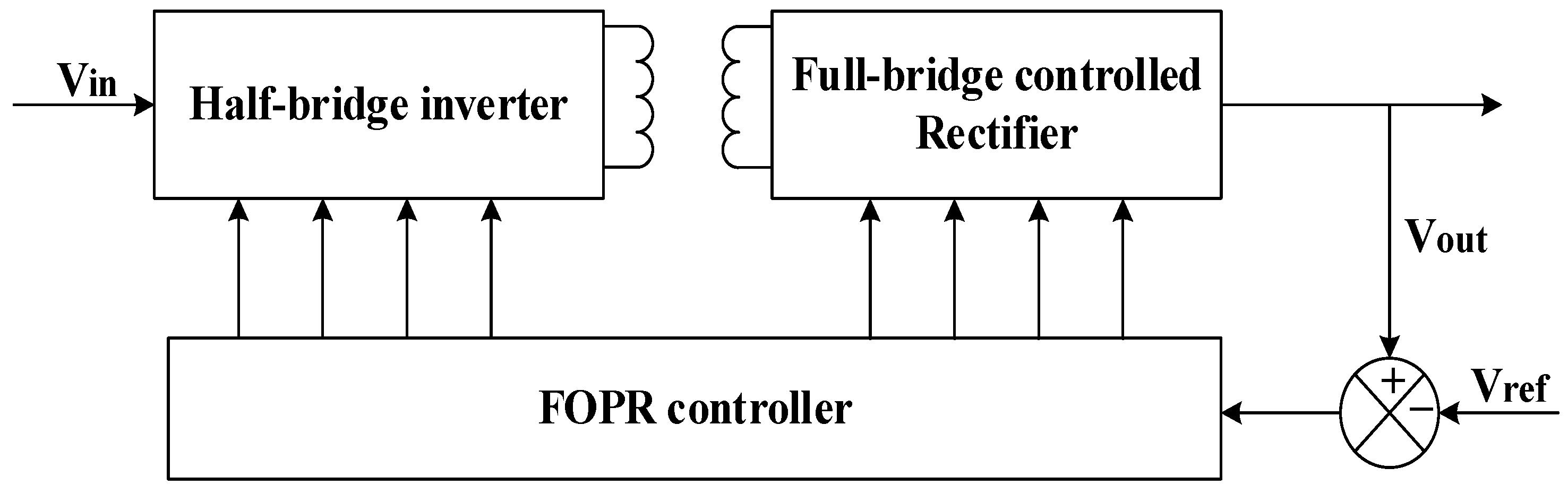
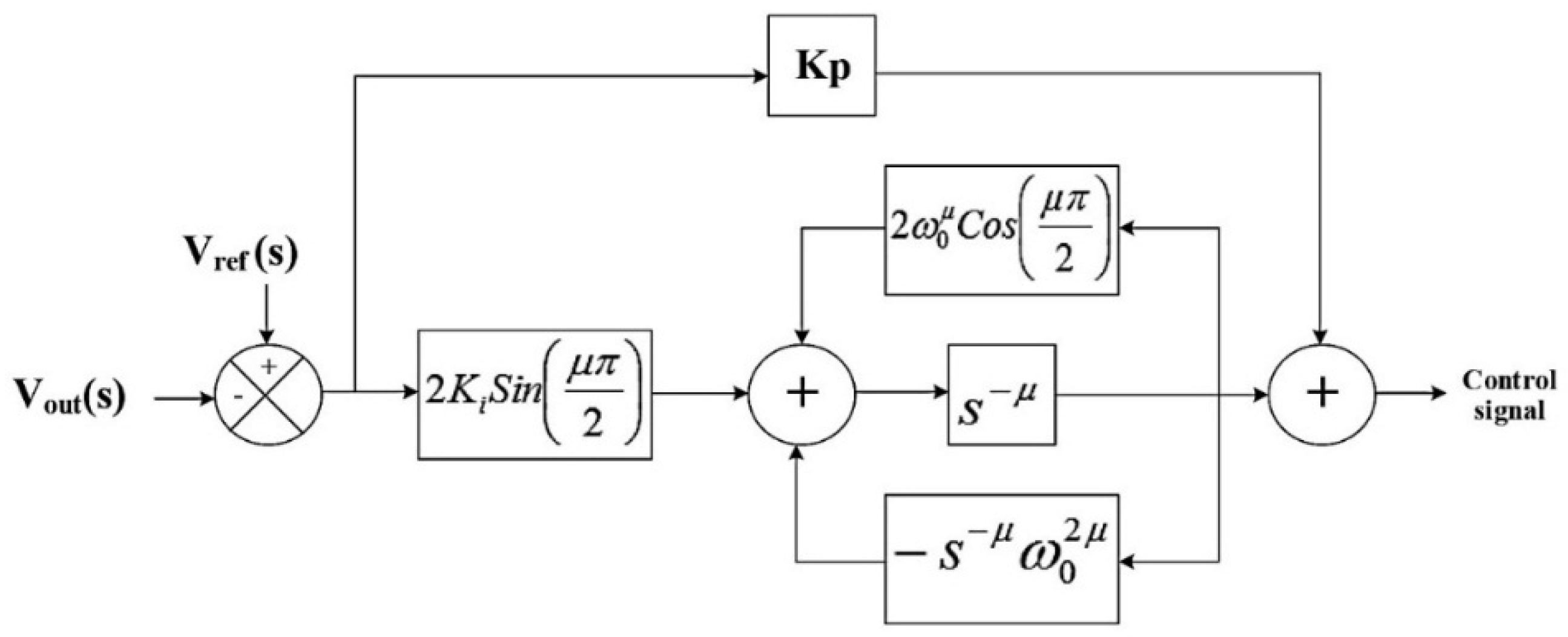
3.6. Control Strategy Using FOPR Controller
3.7. Design Calculation
- ➢
- Output voltage
- ➢
- Leakage reactance of the transformer
- ➢
- Calculation of maximum transformer current
- ➢
- Input inductors
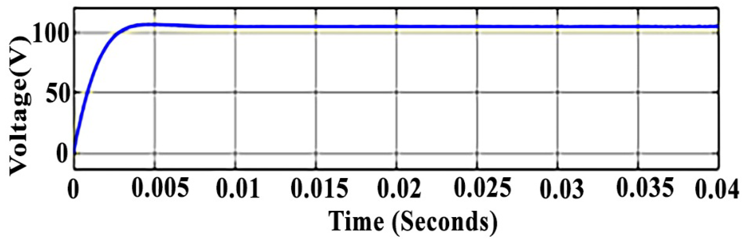
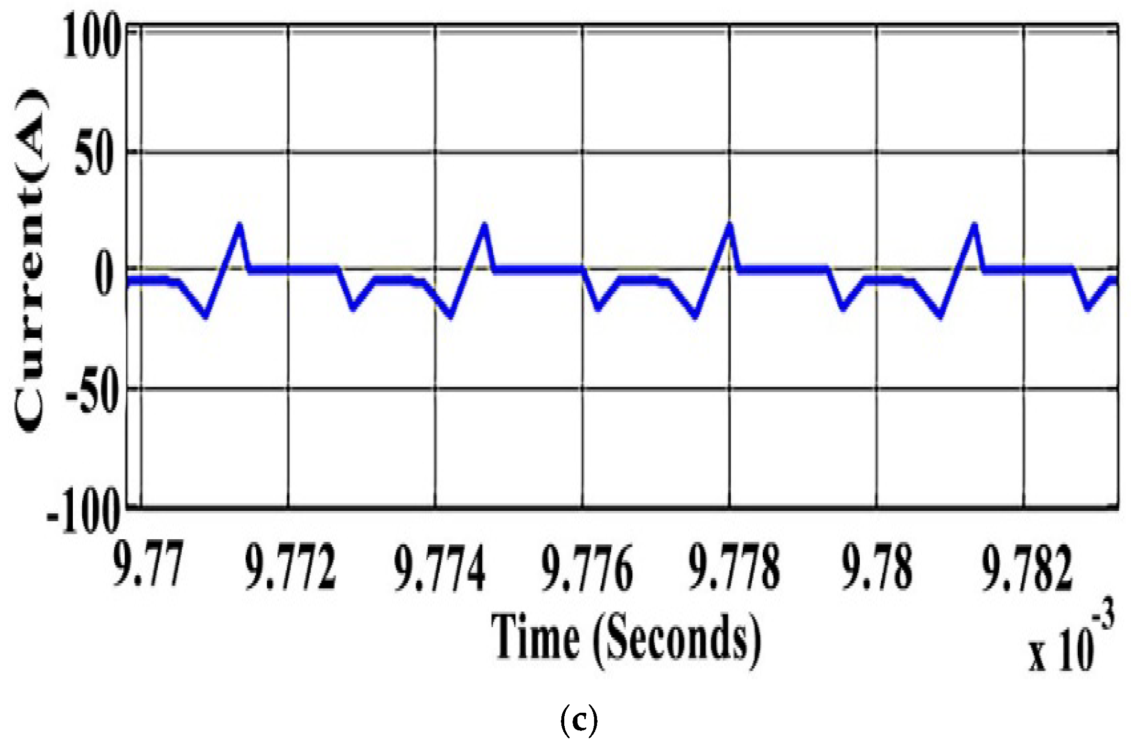
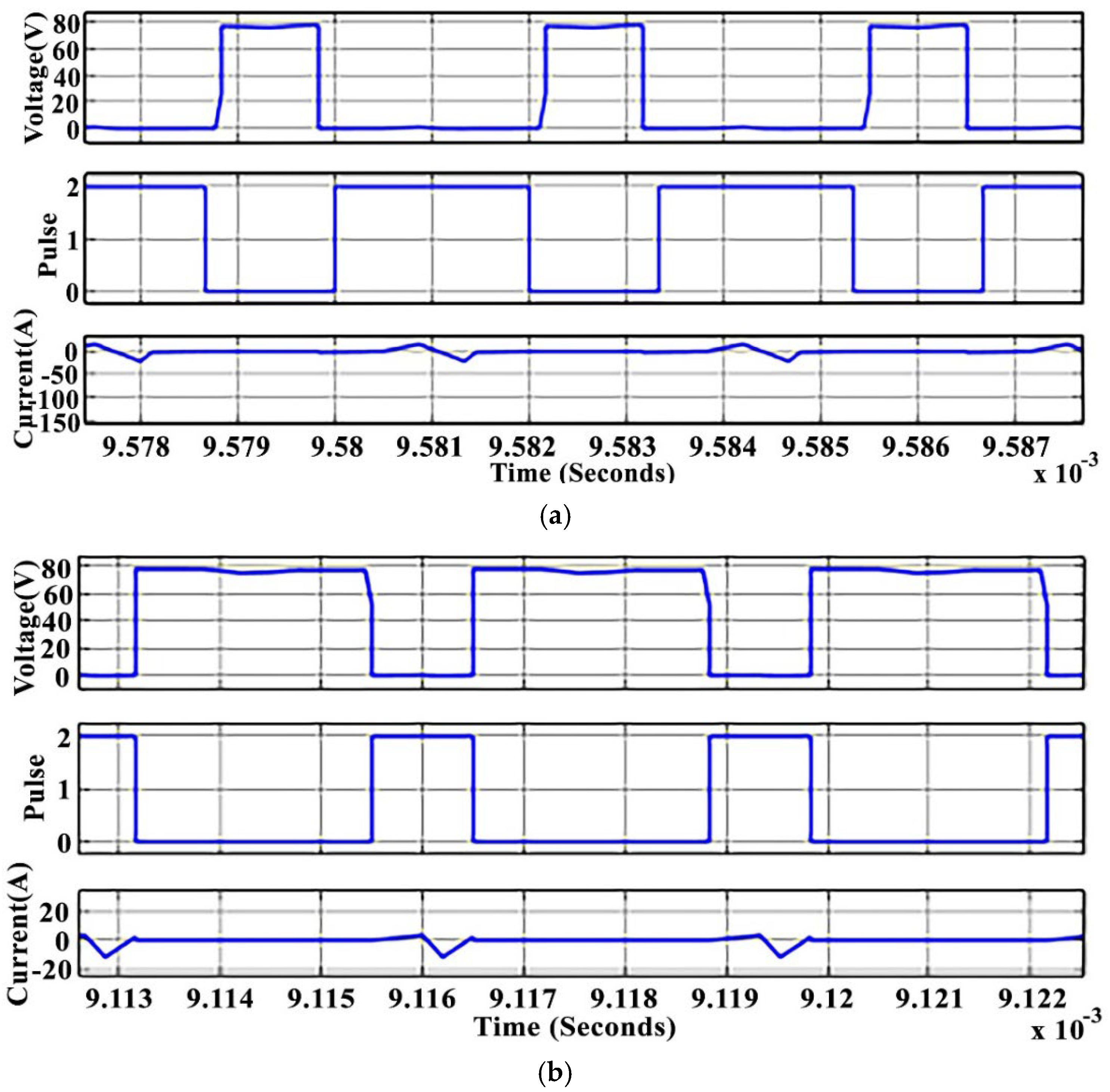
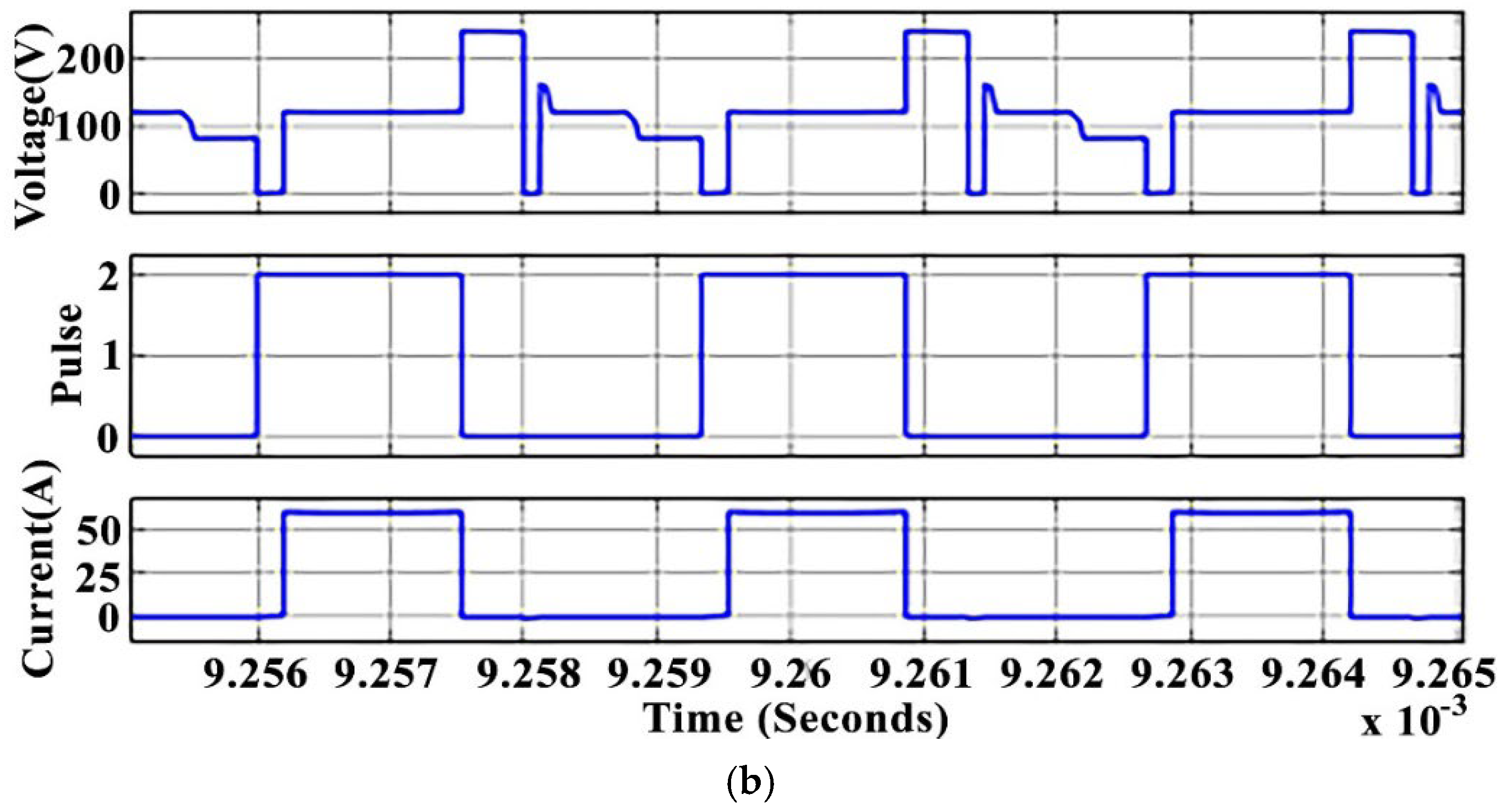
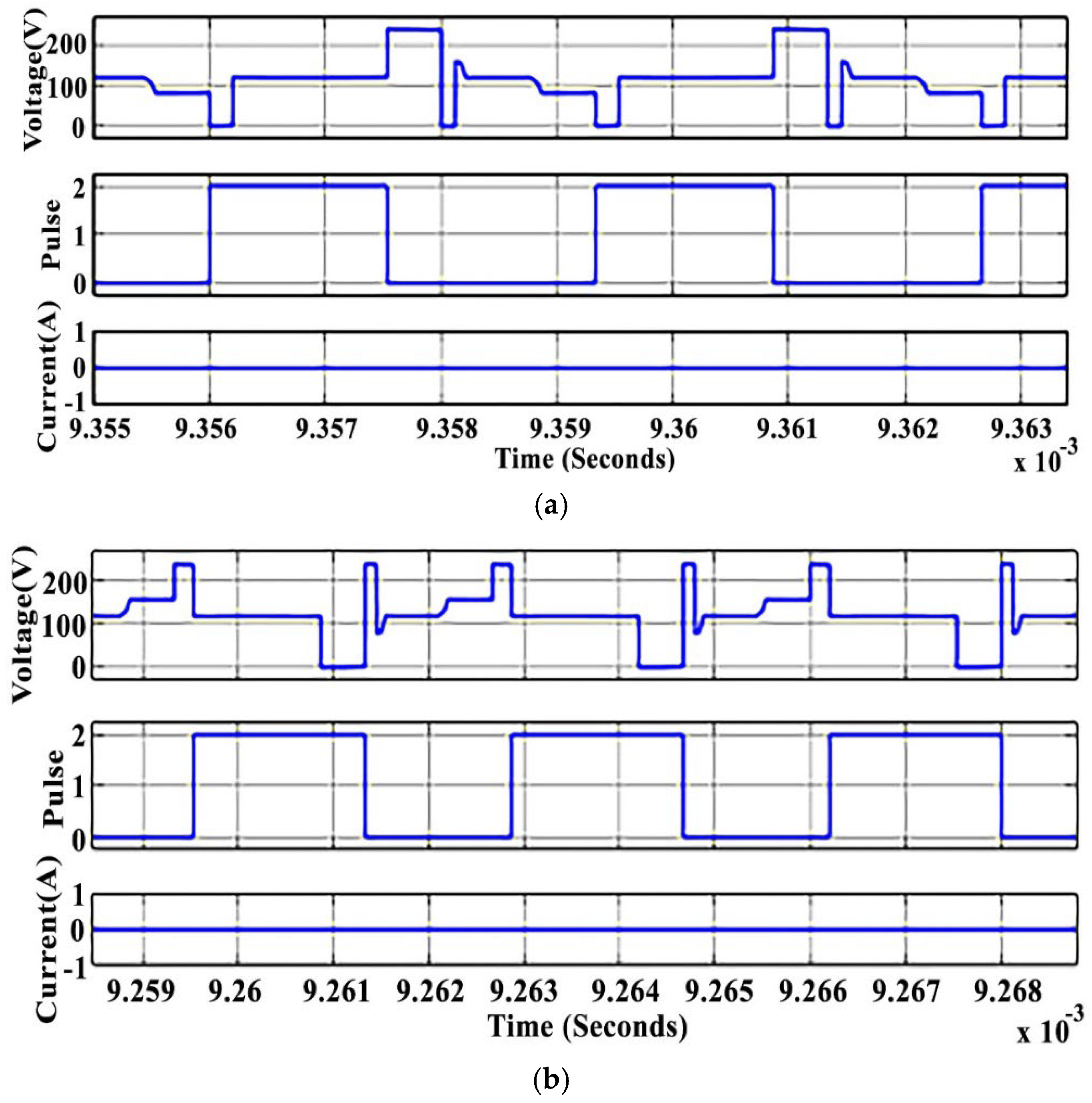
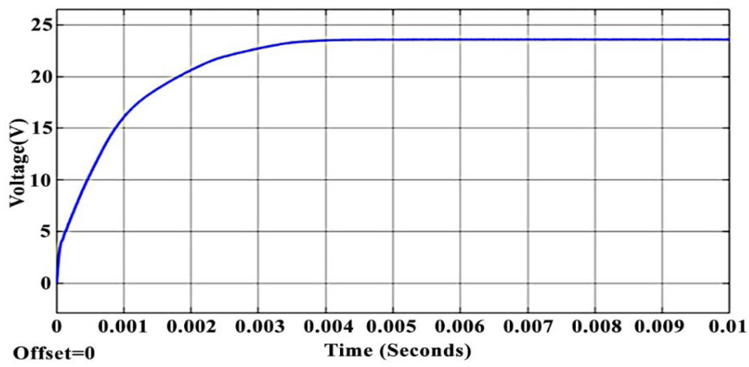
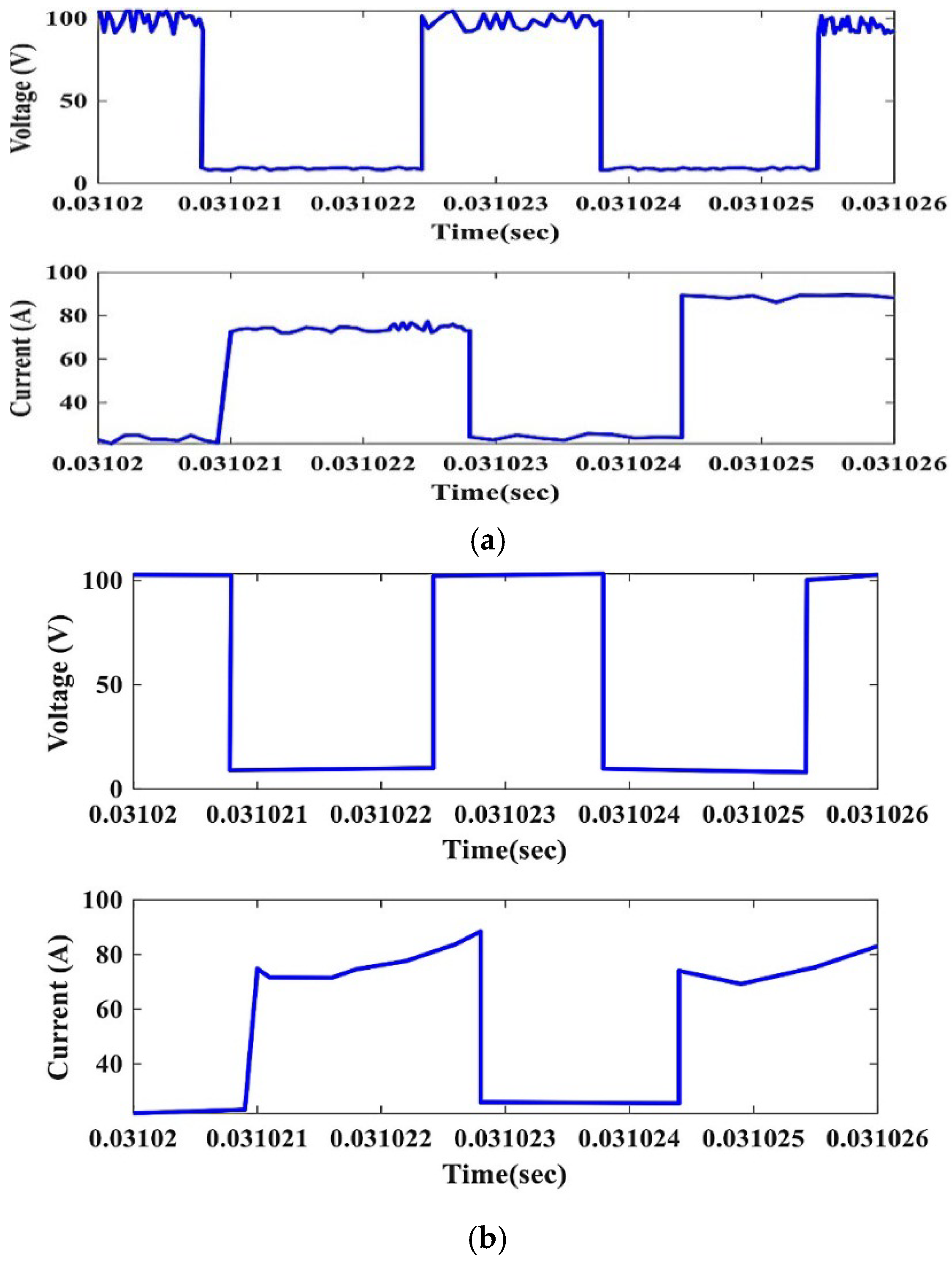
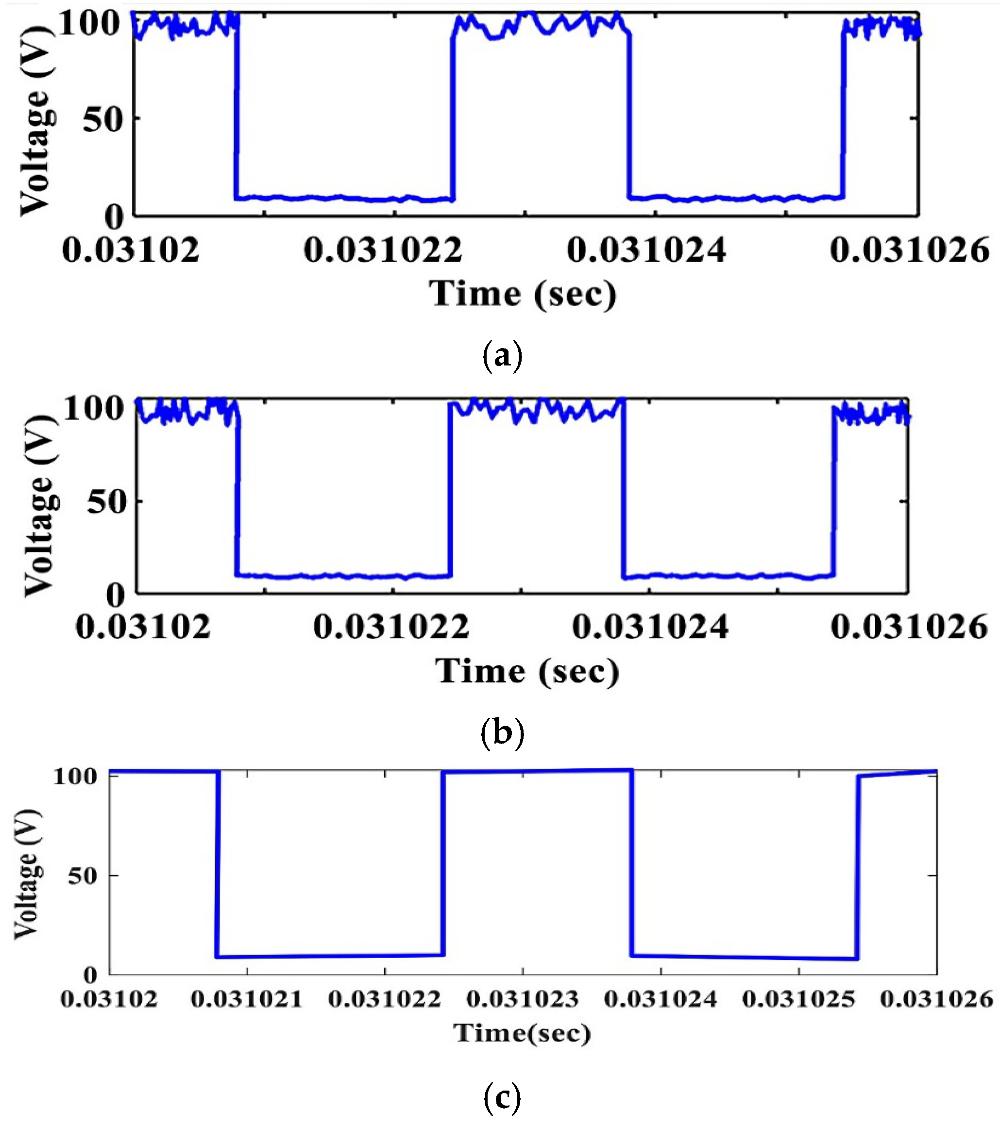
4. Simulation Results
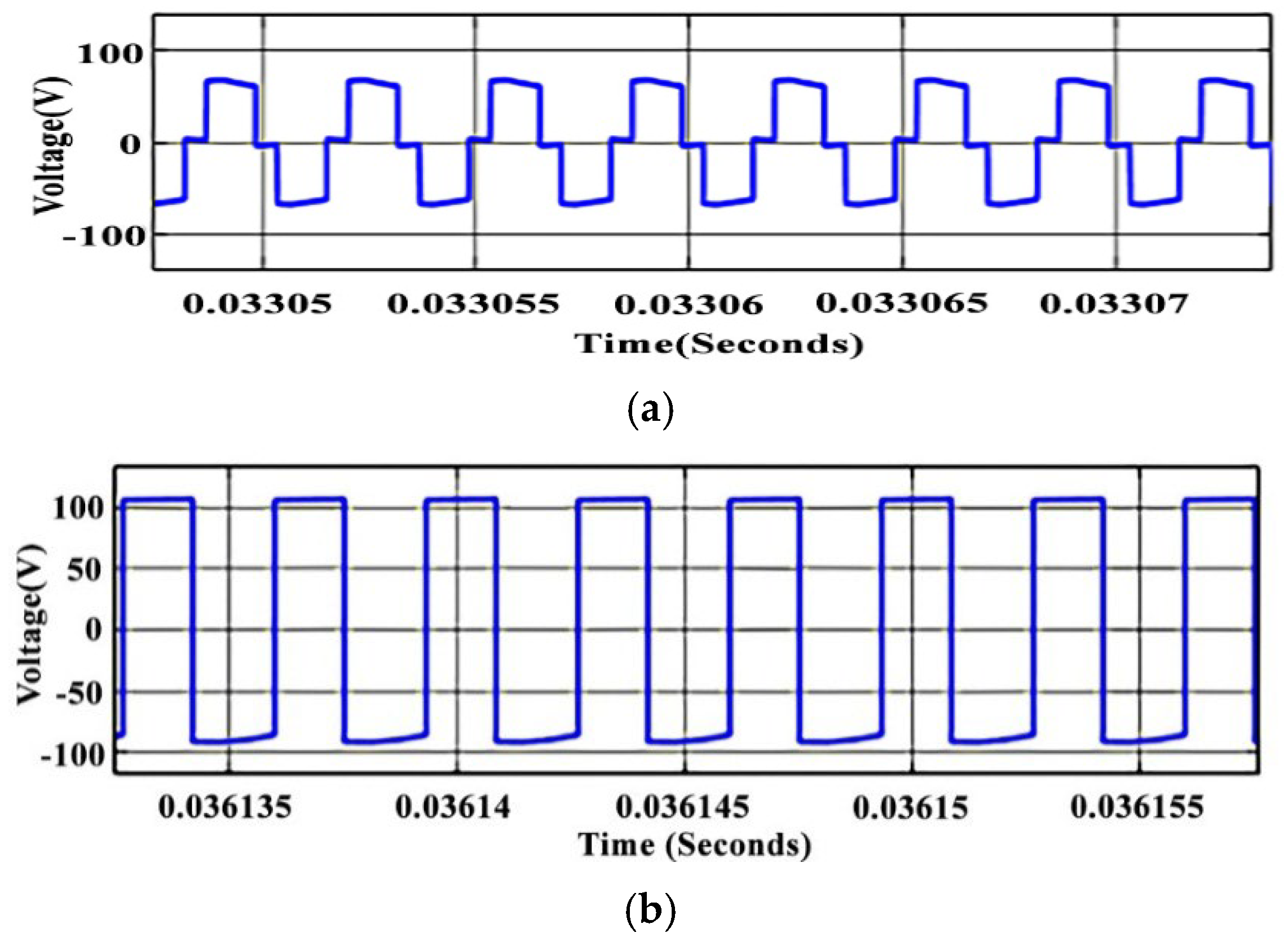
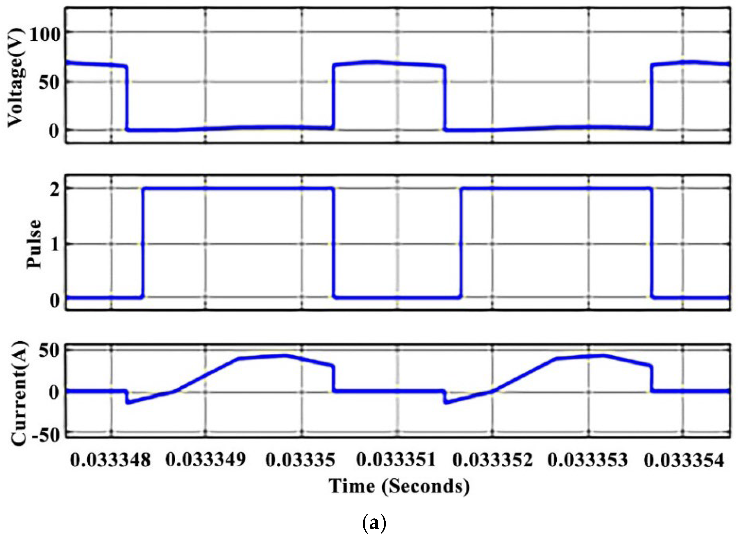
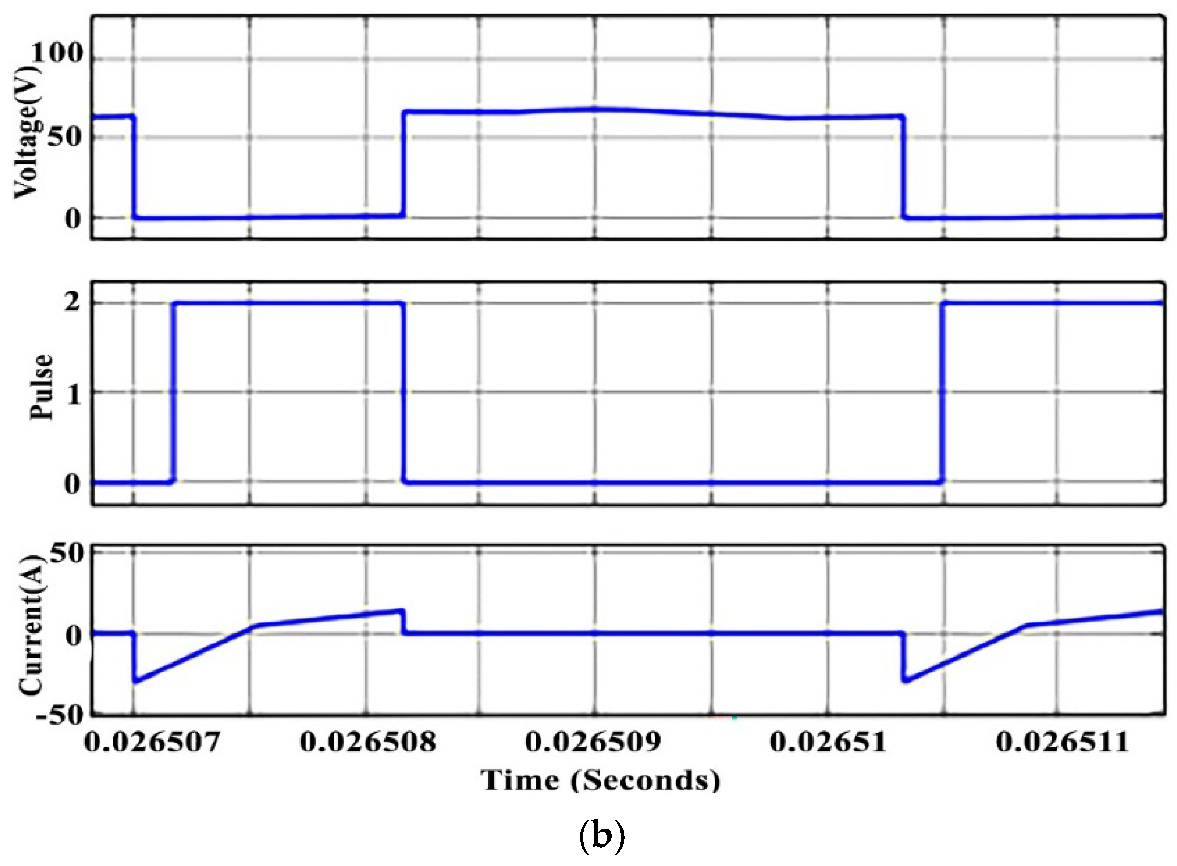
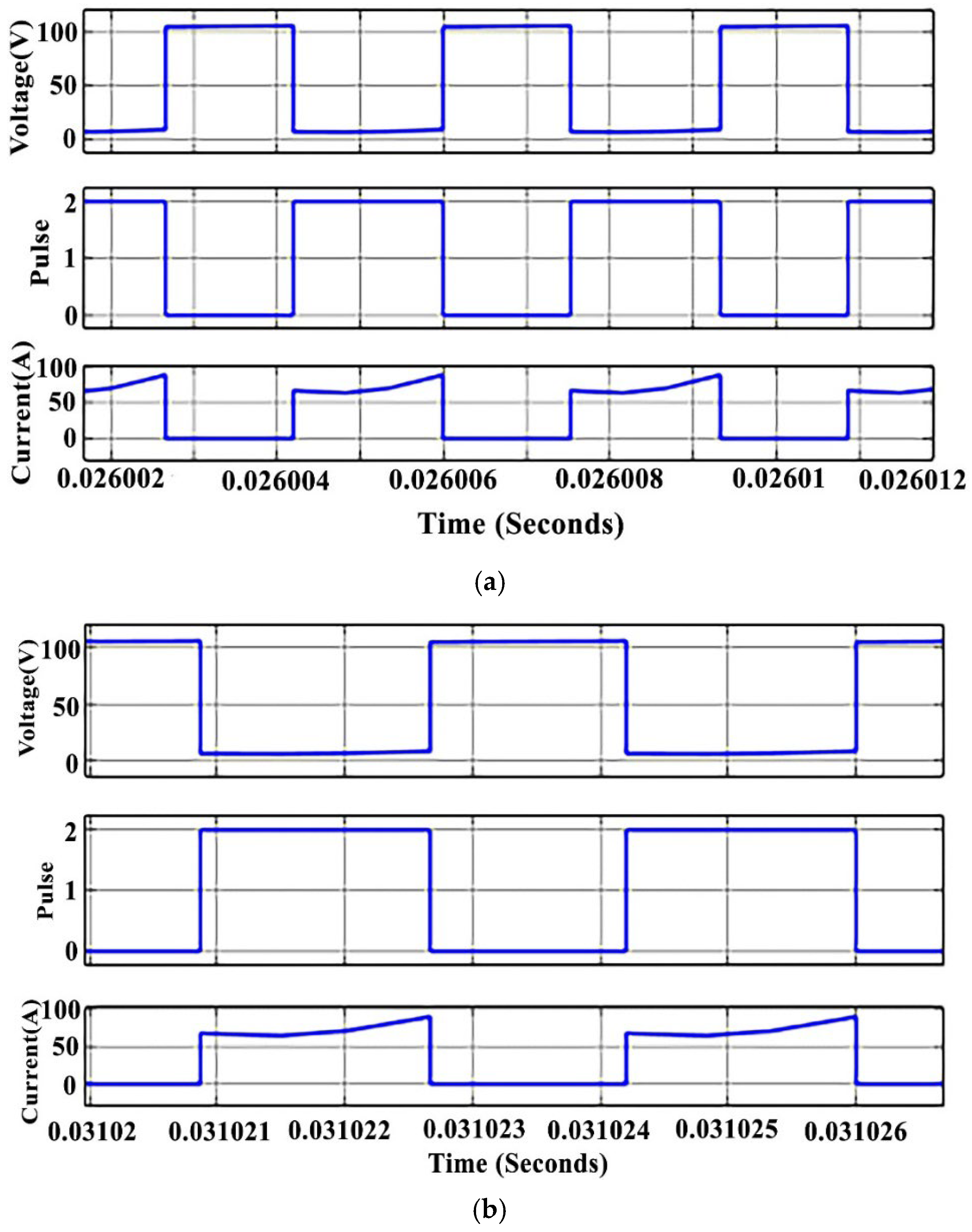
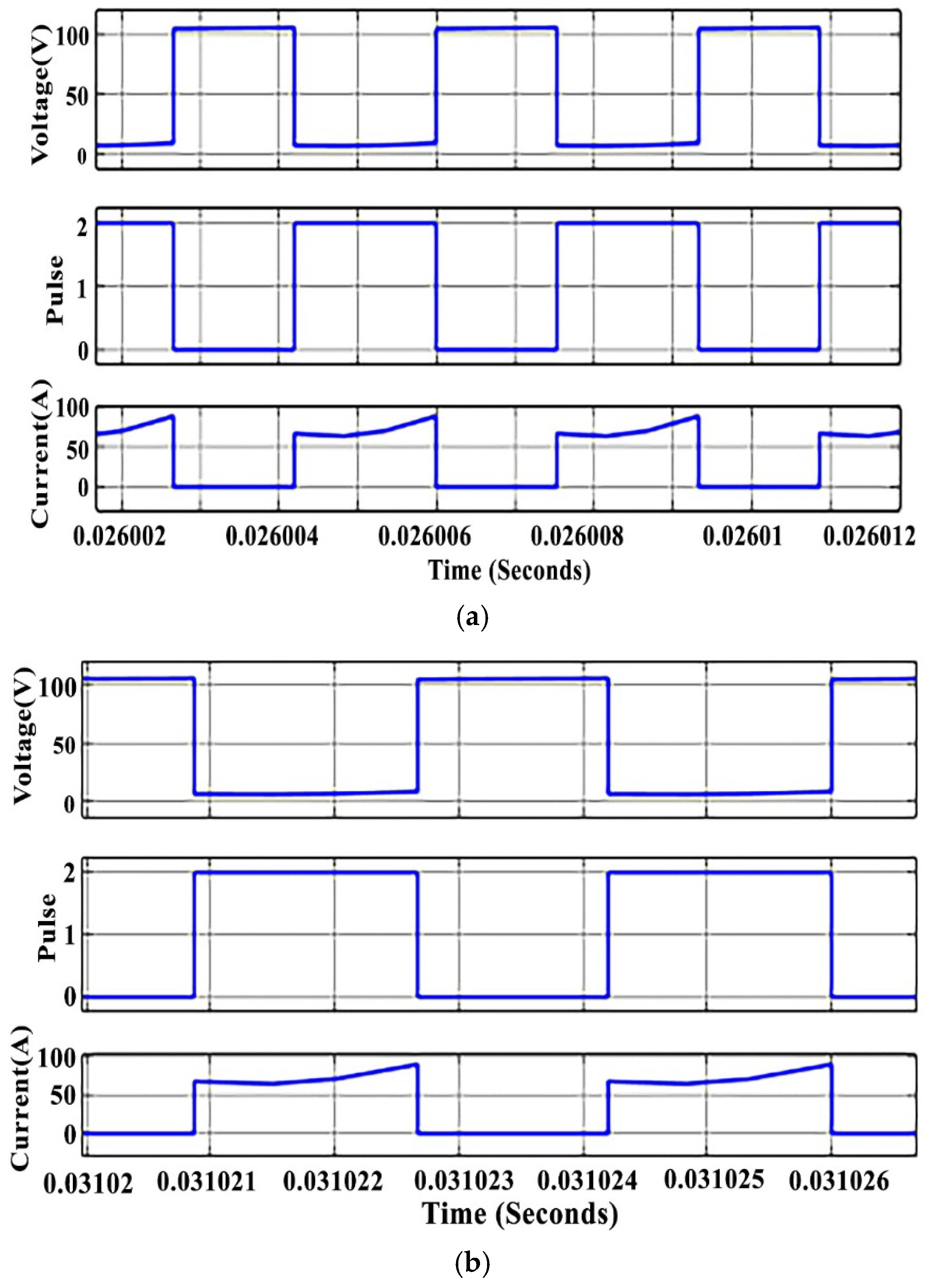
4.1. Discharging Boost Mode
4.2. Recharging Buck Mode
4.3. Discussion
5. Conclusions
Author Contributions
Funding
Data Availability Statement
Conflicts of Interest
References
- Zhang, G.; Li, Z.; Zhang, B.; Halang, W.A. Power electronics converters: Past, present and future. Renew. Sustain. Energy Rev. 2018, 81, 2028–2044. [Google Scholar] [CrossRef]
- Sharma, P.; Dhaked, D.K.; Sharma, A.K. Mathematical modeling and simulation of DC-DC converters using state-space approach. In Proceedings of the Second International Conference on Smart Energy and Communication: ICSEC 2020, Jaipur, India, 20–21 March 2020; Springer: Singapore, 2021; pp. 11–29. [Google Scholar]
- Lu, Y.; Wu, H.; Sun, K.; Xing, Y. A family of isolated buck-boost converters based on semiactive rectifiers for high-output voltage applications. IEEE Trans. Power Electron. 2015, 31, 6327–6340. [Google Scholar] [CrossRef]
- Sharma, P.; Sharma, A.K.; Priyadarshi, N.; Azam, F.; Padmanaban, S.; Bhoi, A.K. A comprehensive study on electrical vehicle in charging infrastructure, challenges and future scope. In Electric Vehicles: Modern Technologies and Trends; Springer: Singapore, 2021; pp. 271–285. [Google Scholar]
- Khan, M.A.; Ahmed, A.; Husain, I.; Sozer, Y.; Badawy, M. Performance analysis of bidirectional DC–DC converters for electric vehicles. IEEE Trans. Ind. Appl. 2015, 51, 3442–3452. [Google Scholar] [CrossRef]
- Rodríguez-Benítez, O.M.; Ponce-Silva, M.; Aquí-Tapia, J.A.; Claudio-Sánchez, A.; Vela-Váldes, L.G.; Lozoya-Ponce, R.E.; Cortés-García, C. Comparative performance and assessment study of a current-fed DC-DC resonant converter combining Si, SiC, and GaN-based power semiconductor devices. Electronics 2020, 9, 1982. [Google Scholar] [CrossRef]
- Dobakhshari, S.S.; Milimonfared, J.; Taheri, M.; Moradisizkoohi, H. A quasi-resonant current-fed converter with minimum switching losses. IEEE Trans. Power Electron. 2016, 32, 353–362. [Google Scholar] [CrossRef]
- Sha, D.; You, F.; Wang, X. A high-efficiency current-fed semi-dual-active bridge DC–DC converter for low input voltage applications. IEEE Trans. Ind. Electron. 2015, 63, 2155–2164. [Google Scholar] [CrossRef]
- Pan, X.; Li, H.; Liu, Y.; Zhao, T.; Ju, C.; Rathore, A.K. An overview and comprehensive comparative evaluation of current-fed-isolated-bidirectional DC/DC converter. IEEE Trans. Power Electron. 2019, 35, 2737–2763. [Google Scholar] [CrossRef]
- Sree, K.R.; Rathore, A.K.; Breaz, E.; Gao, F. Soft-switching non-isolated current-fed inverter for PV/fuel cell applications. IEEE Trans. Ind. Appl. 2015, 52, 351–359. [Google Scholar] [CrossRef]
- Samanta, S.; Rathore, A.K. Wireless power transfer technology using full-bridge current-fed topology for medium power applications. IET Power Electron. 2016, 9, 1903–1913. [Google Scholar] [CrossRef]
- Kosenko, R.; Husev, O.; Chub, A. Full soft-switching high step-up current-fed DC-DC converters with reduced conduction losses. In Proceedings of the 2015 IEEE 5th International Conference on Power Engineering, Energy and Electrical Drives (POWERENG), Riga, Latvia, 11–13 May 2015; IEEE: Piscataway, NJ, USA, 2015; pp. 170–175. [Google Scholar]
- Jin, L.; Liu, B.; Duan, S. ZVS soft switching operation range analysis of three-level dual-active bridge DC–DC converter under phase shift control strategy. IEEE Trans. Ind. Appl. 2018, 55, 1963–1972. [Google Scholar] [CrossRef]
- Xu, X.; Bishop, M.; Oikarinen, D.G.; Hao, C. Application and modeling of battery energy storage in power systems. CSEE J. Power Energy Syst. 2016, 2, 82–90. [Google Scholar] [CrossRef]
- Zhang, Z.; Xie, S.; Shang, X.; Qian, Q.; Xu, J. Modeling and controller optimization for current-fed isolated bidirectional DC–DC converters. J. Power Electron. 2020, 20, 1592–1603. [Google Scholar] [CrossRef]
- Guo, Z.; Sun, K.; Wu, T.F.; Li, C. An improved modulation scheme of current-fed bidirectional DC–DC converters for loss reduction. IEEE Trans. Power Electron. 2017, 33, 4441–4457. [Google Scholar] [CrossRef]
- Kondrath, N. Bidirectional DC-DC converter topologies and control strategies for interfacing energy storage systems in microgrids: An overview. In Proceedings of the 2017 IEEE International Conference on Smart Energy Grid Engineering (SEGE), Oshawa, ON, Canada, 14–17 August 2017; IEEE: Piscataway, NJ, USA, 2017; pp. 341–345. [Google Scholar]
- Zhu, L.; Bai, H.; Brown, A.; Keuck, L. A Current-fed Three-port DC/DC Converter for Integration of On-board Charger and Auxiliary Power Module in Electric Vehicles. In Proceedings of the 2021 IEEE Applied Power Electronics Conference and Exposition (APEC), Phoenix, AZ, USA, 14–17 June 2021; IEEE: Piscataway, NJ, USA, 2021; pp. 577–582. [Google Scholar]
- Weinert, T.; Oberschelp, W.; Schroder, G. A current-fed DC/DC converter for the efficient charging of HV capacitors in mobile applications. In Proceedings of the 2016 18th European Conference on Power Electronics and Applications (EPE’16 ECCE Europe), Karlsruhe, Germany, 5–9 September 2016; IEEE: Piscataway, NJ, USA, 2016; pp. 1–10. [Google Scholar]
- Shi, Y.; Li, R.; Xue, Y.; Li, H. Optimized operation of current-fed dual active bridge DC–DC converter for PV applications. IEEE Trans. Ind. Electron. 2015, 62, 6986–6995. [Google Scholar] [CrossRef]
- Kumar, N.; Panda, S.K. A multipurpose and power quality improved electric vessels charging station for the seaports. IEEE Trans. Ind. Inform. 2022, 19, 3254–3261. [Google Scholar] [CrossRef]
- Kumar, N.; Panda, S.K. Smart High Power Charging Networks and Optimal Control Mechanism for Electric Ships. IEEE Trans. Ind. Inform. 2022, 19, 1476–1483. [Google Scholar] [CrossRef]
- Siu, J.Y.; Kumar, N.; Panda, S.K. Attack detection and mitigation using multi-agent system in the deregulated market. In Proceedings of the 2021 IEEE 12th Energy Conversion Congress & Exposition-Asia (ECCE-Asia), Singapore, 24–27 May 2021; pp. 821–826. [Google Scholar]
- Siu, J.Y.; Kumar, N.; Panda, S.K. Command Authentication Using Multi-agent System for Attacks on the Economic Dispatch Problem. IEEE Trans. Ind. Appl. 2022, 58, 4381–4393. [Google Scholar] [CrossRef]
- Pragaspathy, S.; Rao, R.R.; Karthikeyan, V.; Bhukya, R.; Nalli, P.K.; Korlepara, K.P. Analysis and appropriate choice of power converters for electric vehicle charging infrastructure. In Proceedings of the 2022 2nd International Conference on Artificial Intelligence and Smart Energy (ICAIS), Coimbatore, India, 23–25 February 2022; pp. 1554–1558. [Google Scholar]
- Akhtar, M.F.; Raihan, S.R.; Rahim, N.A.; Akhtar, M.N.; Bakar, E.A. Recent Developments in DC-DC Converter Topologies for Light Electric Vehicle Charging: A Critical Review. Appl. Sci. 2023, 13, 1676. [Google Scholar] [CrossRef]
- Zheng, Y.; Li, S.; Smedley, K.M. Non-isolated high step-down converter with ZVS and low current ripples. IEEE Trans. Ind. Electron. 2018, 66, 1068–1079. [Google Scholar] [CrossRef]
- Liu, Z.; Lin, X.; Gao, Y.; Xu, R.; Wang, J.; Wang, Y.; Liu, J. Fixed-time sliding mode control for DC/DC buck converters with mismatched uncertainties. IEEE Trans. Circuits Syst. I Regul. Pap. 2022, 70, 472–480. [Google Scholar] [CrossRef]
- Shen, X.; Liu, J.; Liu, Z.; Gao, Y.; Leon, J.I.; Vazquez, S.; Wu, L.; Franquelo, L.G. Sliding Mode Control of Neutral-Point-Clamped Power Converters with Gain Adaptation. IEEE Trans. Power Electron. 2024, 39, 9189–9201. [Google Scholar] [CrossRef]
- Sharma, P.; Palwalia, D.K.; Sharma, A.K.; Priyadarshi, N.; Padmanaban, S. Coati optimized FOPID controller for non-isolated DC–DC converters in EV charging application. IET Power Electron. 2024. [Google Scholar] [CrossRef]
- Pramanik, R.; Pati, B.B. Modelling and control of a non-isolated half-bridge bidirectional DC-DC converter with an energy management topology applicable with EV/HEV. J. King Saud Univ.-Eng. Sci. 2023, 35, 116–122. [Google Scholar] [CrossRef]
- Wu, Y.E.; Tai, C.H. Novel Bidirectional Isolated DC/DC Converter with High Gain Ratio and Wide Input Voltage for Electric Vehicle Storage Systems. Batteries 2022, 8, 240. [Google Scholar] [CrossRef]
- Park, H.P.; Kim, M.; Jung, J.H. Bidirectional current-fed CLLC resonant converter employing asymmetric PWM. IEEE Trans. Energy Convers. 2021, 36, 3167–3177. [Google Scholar] [CrossRef]
- Tomar, P.S.; Srivastava, M.; Verma, A.K. An Improved Current-Fed Bidirectional DC–DC Converter for Reconfigurable Split Battery in EVs. IEEE Trans. Ind. Appl. 2020, 56, 6957–6967. [Google Scholar] [CrossRef]
- Wu, F.; Fan, S.; Luo, S. Elimination of Transient Current Mutation and Voltage Spike for Buck–Boost Current-Fed Isolated DC–DC Converter. IEEE Trans. Ind. Electron. 2020, 68, 10928–10937. [Google Scholar] [CrossRef]
- Piasecki, S.; Zaleski, J.; Jasinski, M.; Bachman, S.; Turzyński, M. Analysis of AC/DC/DC Converter Modules for Direct Current Fast-Charging Applications. Energies 2021, 14, 6369. [Google Scholar] [CrossRef]
- Liu, Y.; Chen, C.; Chen, K.; Syu, Y.; Dung, N.A. High-Frequency and High-Efficiency Isolated Two-Stage Bidirectional DC–DC Converter for Residential Energy Storage Systems. IEEE J. Emerg. Sel. Top. Power Electron. 2020, 8, 1994–2004. [Google Scholar] [CrossRef]
- Sharma, A.K.; Vyas, A.; Sharma, P. Comparative study of DC-DC converter with different control techniques. In Proceedings of the Recent Advances in Renewable Energy Sources—RARES2021, Engineering College, Banswara, India, 26–27 February 2021. [Google Scholar]
- Kang, T.; Kim, C.; Suh, Y.; Park, H.; Kang, B.; Kim, D. A design and control of bi-directional non-isolated DC-DC converter for rapid electric vehicle charging system. In Proceedings of the 2012 Twenty-Seventh Annual IEEE Applied Power Electronics Conference and Exposition (APEC), Orlando, FL, USA, 5–9 February 2012; pp. 14–21. [Google Scholar]
- Rahman, M.M.; Uddin, M.N.; Islam, M.K. Performance enhancement of a bi-directional DC-DC converter using a Ćuk converter for electric vehicle applications. In Proceedings of the 2015 IEEE 28th Canadian Conference on Electrical and Computer Engineering (CCECE), Halifax, NS, Canada, 3–6 May 2015; pp. 875–880. [Google Scholar]
- Tandon, S.; Rathore, A.K.; Narasimharaju, B.L. A ZVS series resonant current-fed PWM controlled DC-DC converter. In Proceedings of the 2020 IEEE Transportation Electrification Conference & Expo (ITEC), Chicago, IL, USA, 23–26 June 2020; pp. 320–325. [Google Scholar]
- Malek, H.; Dadras, S.; Yin, C.; Chen, Y.Q. Fractional order proportional-resonant controller. In Proceedings of the 2018 Annual American Control Conference (ACC), Milwaukee, WI, USA, 27–29 June 2018; IEEE: Piscataway, NJ, USA, 2018; pp. 3086–3091. [Google Scholar]
- Wu, Y.E.; Ke, Y.T. A novel bidirectional isolated DC-DC converter with high voltage gain and wide input voltage. IEEE Trans. Power Electron. 2020, 36, 7973–7985. [Google Scholar] [CrossRef]
- Packnezhad, M.; Farzanehfard, H. Soft-switching high step-up/down converter using coupled inductors with minimum number of components. IEEE Trans. Ind. Electron. 2020, 68, 7938–7945. [Google Scholar] [CrossRef]
- Mohammadi, M.R.; Amoorezaei, A.; Khajehoddin, S.A.; Moez, K. A high step-up/step-down LVS-parallel HVS-series ZVS bidirectional converter with coupled inductors. IEEE Trans. Power Electron. 2021, 37, 1945–1961. [Google Scholar]
- Shu, L.; Chen, W.; Shi, M.; Liu, R.; Gao, S.; Deng, F. Improved Control Strategy of Triple-Voltage Three-Phase DAB (T 2-DAB) Converter for Current Stress and Zero-Voltage-Switching Optimization. IEEE J. Emerg. Sel. Top. Power Electron. 2021, 10, 773–784. [Google Scholar] [CrossRef]
- Cúnico, L.M.; Alves, Z.M.; Kirsten, A.L. Efficiency-optimized modulation scheme for three-phase dual-active-bridge DC–DC converter. IEEE Trans. Ind. Electron. 2020, 68, 5955–5965. [Google Scholar] [CrossRef]


| Mode Number | Duration (s) | Conduction | Turn ON | Turn OFF |
|---|---|---|---|---|
| Mode 0 | - | - | ||
| Mode 1 | - | |||
| Mode 2 | - | |||
| Mode 3 | - | |||
| Mode 4 | - | |||
| Mode 5 | - | |||
| Mode 6 | - |
| Parameter | Symbol | Value |
|---|---|---|
| Input voltage | 25 V | |
| Output voltage | 111 V | |
| Switching frequency | 100 kHz | |
| Transformation ratio | N1: N2 | 1:2 |
| Input inductance | 8.5 µH | |
| Input inductance | 8.5 µH | |
| Leakage reactance | 90 µH | |
| Clamping capacitor | 2.6 µF | |
| Output capacitor | 10 µF | |
| Duty cycle | 0.55 | |
| Proportional constant | 0.5 | |
| Integral constant | 0.6 | |
| Fractional order | 0.6 | |
| Selected angular frequency | rad/s |
Disclaimer/Publisher’s Note: The statements, opinions and data contained in all publications are solely those of the individual author(s) and contributor(s) and not of MDPI and/or the editor(s). MDPI and/or the editor(s) disclaim responsibility for any injury to people or property resulting from any ideas, methods, instructions or products referred to in the content. |
© 2024 by the authors. Licensee MDPI, Basel, Switzerland. This article is an open access article distributed under the terms and conditions of the Creative Commons Attribution (CC BY) license (https://creativecommons.org/licenses/by/4.0/).
Share and Cite
Sharma, P.; Palwalia, D.K.; Sharma, A.K.; Gopal, Y.; Rosas-Caro, J.C. Novel Current-Fed Bidirectional DC-DC Converter for Battery Charging in Electric Vehicle Applications with Reduced Spikes. Electricity 2024, 5, 1022-1048. https://doi.org/10.3390/electricity5040052
Sharma P, Palwalia DK, Sharma AK, Gopal Y, Rosas-Caro JC. Novel Current-Fed Bidirectional DC-DC Converter for Battery Charging in Electric Vehicle Applications with Reduced Spikes. Electricity. 2024; 5(4):1022-1048. https://doi.org/10.3390/electricity5040052
Chicago/Turabian StyleSharma, Piyush, Dheeraj Kumar Palwalia, Ashok Kumar Sharma, Yatindra Gopal, and Julio C. Rosas-Caro. 2024. "Novel Current-Fed Bidirectional DC-DC Converter for Battery Charging in Electric Vehicle Applications with Reduced Spikes" Electricity 5, no. 4: 1022-1048. https://doi.org/10.3390/electricity5040052
APA StyleSharma, P., Palwalia, D. K., Sharma, A. K., Gopal, Y., & Rosas-Caro, J. C. (2024). Novel Current-Fed Bidirectional DC-DC Converter for Battery Charging in Electric Vehicle Applications with Reduced Spikes. Electricity, 5(4), 1022-1048. https://doi.org/10.3390/electricity5040052