1. Introduction
Radon gas (Rn-222) is a noble, odorless, invisible, and chemically inert radioactive gas that emerges naturally from soils and rocks. It represents one of the main sources of exposure to radioactivity in humans, as it emits alpha particles that may damage lung tissues after inhalation [
1]. It is by now well-established that radon gas is the second most important cause of lung cancer and the most important cause of lung cancer in non-smokers, while every 1 in 15 homes in the US suffers from high level of radon concentration [
2,
3].
The commercial solid state semiconductor radon sensors are reviewed in [
4,
5] and are implemented in PIN diodes. Low dark current PIN diodes are expensive since large area photodiodes often have defects leading to large dark currents; thus, the sensors are expensive.
The goals of this study were to specify the requirements for Radon gas sensors for smart homes and report how to meet these requirements. It is obvious that for consumer applications, the sensor must be low-cost, small, require low power, and exhibit high sensitivity and reliability. It is obvious to the authors that a standard CMOS technology is mandatory, and a transistor will exhibit higher sensitivity than a PIN diode.
The innovation of the new sensor, dubbed TODOS-Radon Sensor is outlined in the sections below:
Section 2.3 presents the new sensor and system architecture and innovations. Device characterization is reported in
Section 3.1.
Section 3.2 presents experimental results of Radon gas exposure.
Section 4 concludes this study.
2. Materials and Methods
2.1. Floating Gate Transisor
The operation principle to sense radiation using Floating Gate (FG) transistor is to first pre-charge the FG using Fowler–Nordheim (FN) Tunneling by applying a large enough electric field on the FG itself [
6]. Once the FG is charged, an alpha particle incident will generate e–h pairs that will be separated by an applied electrical field and will discharge the FG [
7]. Considering the fact that the threshold voltage of the device is proportional to the charge within the FG as described by Equation (1), an alpha incident will shift the device’s threshold voltage as illustrated in
Figure 1.
where
is the combined work function difference,
and
are the fixed charge densities in the read out oxide and in the control oxide respectively and
is the serial oxide-STI capacitance, given by (see
Figure 1a):
is the number of generated
e–
h pairs by a single alpha incident,
A is the sensing capacitor area and
is the sensing capacitor thickness.
The number of e–h pairs generated by an alpha incident-
, can be calculated by dividing the absorbed energy of a single alpha particle with the e–h pair generation energy. In the proposed Radon Sensor, the STI layer thickness is
. The absorbed energy is calculated using popular SRIM software [
8]. As shown in
Figure 2e–h pair generation energy in
is 17 eV [
9].
The total absorbed energy within the STI layer is 53.7 KeV, so the number of e–h pairs produced by an alpha particle is:
2.2. C-Sensor
Fabricating an FG transistor in standard CMOS process with a single polysilicon layer was done in the mature, well-proven TowerJazz High Voltage standard 180 nm CMOS Process [
10]. TowerJazz had been developing Floating-Gate technology for memory devices, which had been later further developed and extended for direct sensing of radiation and dubbed C-cell. This technology and its reliability have been documented in the open literature [
11,
12,
13,
14,
15,
16]. The essence of this technology is shown in
Figure 3.
2.3. System Implementation
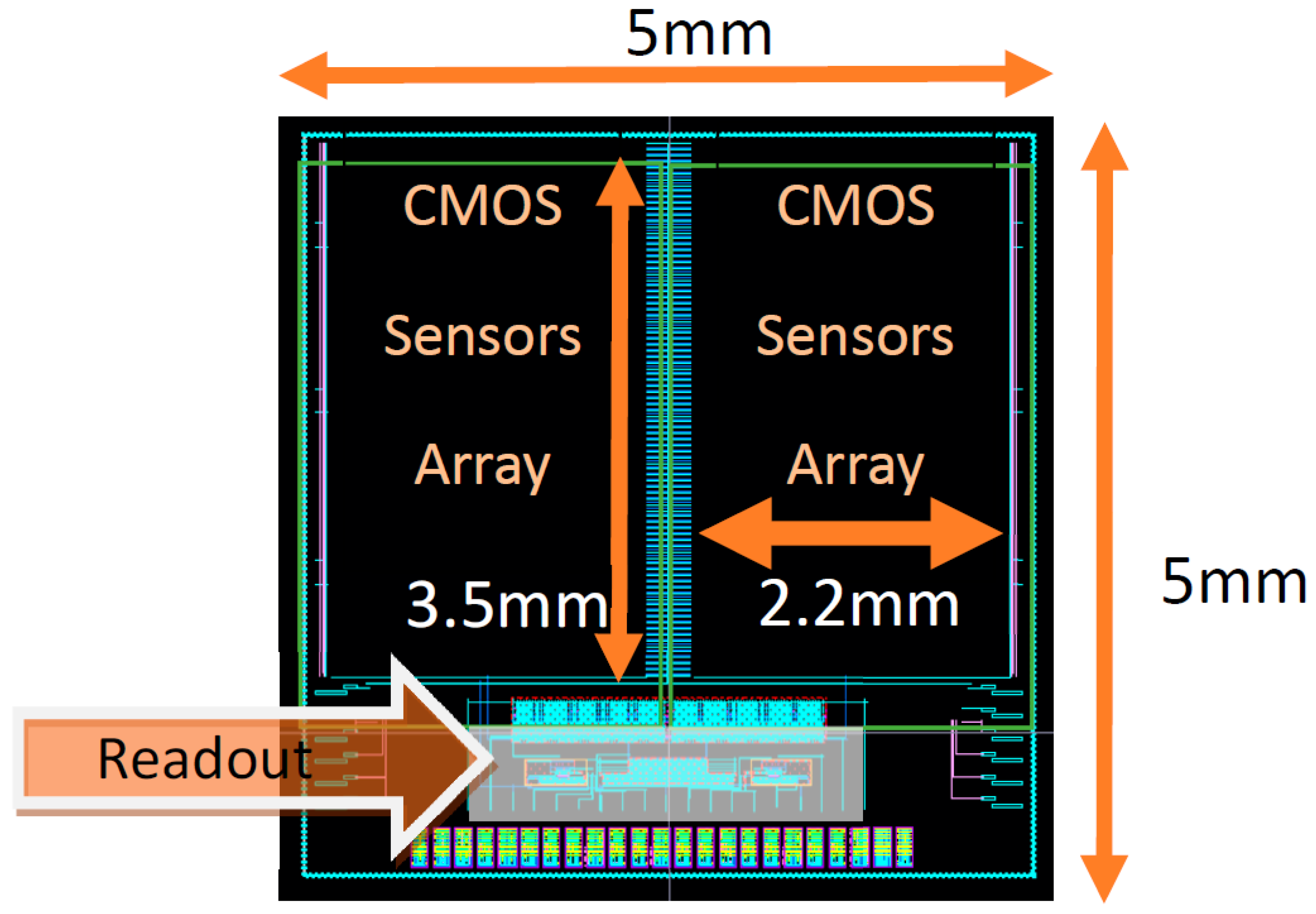
A way to effectively increase the sensing area of the device while keeping high yield, is by using a mosaic array of C-Sensors, where all cells are connected in parallel as shown in
Figure 4. Each cell in the mosaic array is considered as sub-pixel. Although a defect in a single sub-pixel will disable the sub-pixel itself, it will be negligible considering that there are thousands of sub-pixels.
The sensors array is built by sub-pixels, where each sub-pixel sensing area is , so that the entire array sensing area is .
In order to decrease DC and temperature dependencies, a differential measurement is performed using the concept of active and blind sensor arrays. Considering that alpha particle is a heavy particle, meaning its penetration depth is relatively small, few layers of Kapton film (~
) were used to cover one of the arrays so it could be considered as a blind detector. The device layout is shown in
Figure 5.
Another key concept in the proposed architecture is operating in the sub-threshold region, decreasing the power and noise, and also increasing the sensitivity due to the exponential relation
at subthreshold.
Operating in the subthreshold region introduces a linear relation between the output signal and the bias current—. This point is used as a feature to configure the sensitivity of the device, adapting it to long/short term measurements.
Since the power consumption of the device is dominated by the bias current of the sub-pixels, working in the subthreshold will result in low power consumption which will enable the device to be operated by standard AAA batteries.
An incident alpha particle on the active sensors array will increase current as shown in Equation (5). Subtracting the blind array’s current from the active array’s current provides a differential measurement. Hence, the readout circuit was designed as a precise current subtractor followed by a Trans Impedance Amplifier (TIA), to convert the output signal into output voltage (see
Figure 6). The difference between two adjacent samples of the readout voltage, meaning the output voltage derivative, reflects the amount of alpha particles incidents.
Considering Equation (3), the threshold shift of a single sub-pixel caused by a single alpha incident is given in Equation (6).
So that the average threshold voltage shift of the entire array is:
3. Results
3.1. Device Characterization
As the first part of the device characterization, the charging mechanism was tested to achieve controllability over the threshold voltage of each sensor array.
Figure 7 shows an initial calibration process to shift the sub-pixels threshold voltage into higher and positive values.
The need to have such controllability over the threshold voltage comes from the need to: (a) minimize the offset between the arrays, keeping the readout circuit out of saturation, (b) configure high threshold voltage, to increase the e–h separation ratio, and (c) perform a sort of reset stage once the readout circuit is close to saturation.
To characterize the device response to alpha particles radiation, the device was exposed to an alpha source, Po-210, with an alpha emission rate of 925 Bq for two periods of 6 min, with a reset stage before each exposure.
The number of alpha particles reaching the detector is given by:
where
is the detector active sensing area and R is the distance of the detector from the alpha source. Incident alpha ratio is calculated to be
, so that the expected threshold voltage shift can be calculated by multiplying the threshold voltage shift caused by a single alpha incident, with the number of alpha particles reaching the detector:
Figure 8 describes the experiment flow and the threshold voltage shift.
Table 1 summarizes the results over three different devices, where each device was exposed twice to the alpha source, while a reset stage was performed before each exposure (see
Figure 9).
Table 1 indicates the bias current of the active device in each exposure, the threshold voltage shift and the readout voltage change through the exposure.
3.2. Radon Gas Exposure
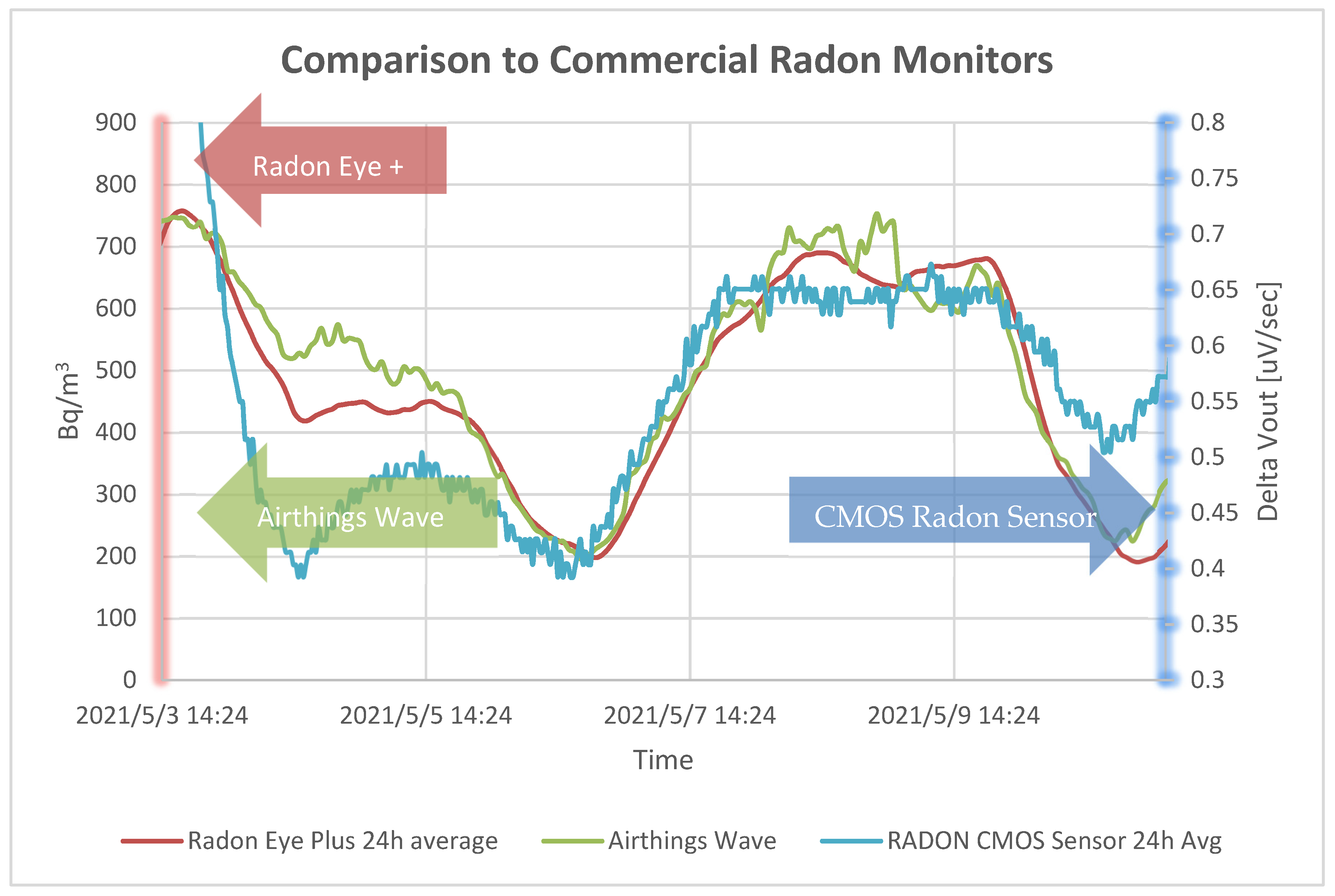
Four instances of the proposed radon sensors were exposed to radon gas in concentrations of up to for two periods of 9 days and 7 days respectively. The sensor results were compared with commercial detectors: Radon Eye plus and Airthings wave.
Figure 10 presents 27 mV threshold voltage shift after 9 days of radon exposure for a single sensor, while
Figure 11 presents the readout circuit derivative of all instances, which represents the voltage difference between two measures caused by alpha particles incident on the active detector. All instances present the same trend, while the distribution of the results reflects each sensor’s sensitivity, which is configured by the sensor’s bias current.
Figure 12 shows the comparison between commercial radon sensors to the proposed CMOS sensor. In order to convert the readout voltage into radon concentration, a calibration factor is suggested:
Calculating the calibration factor for the compared device in
Figure 12, is given by:
Figure 13 shows radon measurement of a different CMOS sensor device, with a higher sample rate, at a different period of time. Calibration factor is extracted again:
4. Conclusions
A new sensing system for detecting high energy alpha particle and Radon gas is reported. The system is based on a CMOS IC Sensor which was fabricated in a standard CMOS process with a single polysilicon layer. The sensor’s unique architecture is based on active and blind mosaic arrays of FG cells, operating in sub threshold region.
The sensing system was tested by exposure to an alpha radiation source in a controlled environment as well as to Radon gas and showed high sensitivity and good correlation to other commercial radon detectors.
In summary, the main advantages of the new Sensing System are: low cost compared to commercial radon sensors, enabling it to be applied in every smart home; low power and may be battery operated using standard AAA batteries; and the integrated digital sensor allows for continuous sampling of radon gas in indoor air providing hourly resolution of Radon levels. The CMOS die is passivated, and therefore insensitive to humidity.
5. Patents
Technion-TODOS Ltd. Patent Application; # provisional July 2019, Current July 2021.
Author Contributions
Conceptualization, Y.N.; methodology, Y.N. and R.S.; software, R.S.; validation, R.S.; formal analysis, Y.N. and R.S.; investigation, Y.N. and R.S.; writing—original draft preparation, R.S.; writing—review and editing, Y.N. and R.S.; supervision, Y.N.; project administration, Y.N.; funding acquisition, Y.N. Both authors have read and agreed to the published version of the manuscript.
Funding
This research was funded by TODOS TECHNOLOGIES Ltd. (
https://www.todos-technologies.com, (accessed on 1 August 2021)) TODOS TECHNOLOGIES holds exclusively the IP related to this work, Technion grant number “2024790”. The die fabrication was funded by TowerJazz. The patents related to the technology of fabrication are held exclusively by TowerJazz.
Institutional Review Board Statement
Not applicable.
Informed Consent Statement
Not applicable.
Data Availability Statement
Not applicable.
Acknowledgments
The authors would like to thank all the people who contributed to this work: Igor Brouk, Tanya Blank, Sara Stolyarova, Sharon Bar-Lev, and Gavriel Amar. Last but not least, the enormous contribution of Lena Zugman, the library of the ECE Dept. at Technion-Israel Institute of Technology is appreciated.
Conflicts of Interest
The authors declare no conflict of interest. Roy Shor pursued this research as part of his M.Sc. thesis at Technion- Israel Institute of Technology. Yael Nemirovsky supervised the research and thesis.
References
- Kutz, M. Handbook of Environmental Engineering, 1st ed.; John Wiley & Sons: Hoboken, NJ, USA, 2018; pp. 546–553. [Google Scholar]
- US Environmental Protection Agency. A Citizen’s Guide to Radon: The Guide to Protecting Yourself and Your Family from Radon. Available online: https://www.epa.gov/radon/citizens-guide-radon-guide-protecting-yourself-and-your-family-radon (accessed on 17 September 2021).
- Suzuki, G.; Yamaguchi, I.; Ogata, H.; Sugiyama, H.; Yonehara, H.; Kasagi, F.; Fujiwara, S.; Tatsukawa, Y.; Mori, I.; Kimura, S. A nation-wide survey on indoor radon from 2007 to 2010 in Japan. J. Radiat. Res. 2010, 51, 683–689. [Google Scholar] [CrossRef] [PubMed] [Green Version]
- Kim, J.H.; Yun, S.H.; Kim, G.S. Accuracy Improvement of a PIN Photodiode Radon Counter. Int. J. Innov. Sci. Eng. Technol. 2017, 4, 129–133. [Google Scholar]
- Hofmann, M.; Richter, M.; Jann, O. Use of commercial radon monitors for low level radon measurements in dynamically operated VOC emission test chambers. Radiat. Prot. Dosim. 2017, 177, 16–20. [Google Scholar] [CrossRef] [PubMed]
- Pavan, P.; Larcher, L.; Marmiroli, A. Floating Gate Devices: Operation and Compact Modeling, 1st ed.; Springer Science: Boston, MA USA, 2004; pp. 24–29. [Google Scholar]
- Cellere, G.; Paccagnella, A.; Larcher, L.; Chimenton, A.; Wyss, J.; Candelori, A.; Modelli, A. Anomalous charge loss from floating-gate memory cells due to heavy ions irradiation. IEEE Trans. Nucl. Sci. 2002, 49, 3051–3058. [Google Scholar] [CrossRef]
- SRIM—The Stopping and Range of Ions in Matter. Available online: http://www.srim.org/ (accessed on 1 August 2021).
- Ausman, G.A., Jr.; McLean, F.B. Electron-Hole pair Creation Energy in SiO2. Appl. Phys. Lett. 1975, 26, 173–175. [Google Scholar] [CrossRef]
- TowerJazz–Radiation and UV Sensors. Available online: https://towersemi.com/technology/non-imaging-sensors/radiation-sensors (accessed on 1 August 2021).
- Pikhay, E.; Roizin, Y.; Nemirovsky, Y. Degradation study of single poly radiation sensors by monitoring charge trapping. Microelectron. Reliab. 2016, 59, 18–25. [Google Scholar] [CrossRef]
- Pikhay, E.; Roizin, Y.; Nemirovsky, Y. Ultra-low power consuming direct radiation sensors based on floating gate structures. J. Low Power Electron. Appl. 2017, 7, 20. [Google Scholar] [CrossRef]
- Villani, E.G.; Crepaldim, M.; DeMarchi, D.; Gabrielli, A.; Khan, A.; Pikhay, E.; Roizin, Y.; Rosenfeld, A.; Zhang, Z. A monolithic 180 nm CMOS dosimeter for wireless In Vivo Dosimetry. Radiat. Meas. 2016, 84, 55–64. [Google Scholar] [CrossRef]
- Pikhay, E.; Roizin, Y.; Gatti, U.; Calligaro, C. Re-usable 180 nm CMOS dosimeter based on a floating gate device. In Proceedings of the IEEE International Conference on Electronics, Circuits and Systems (ICECS), Monte Carlo, Monaco, 11–14 December 2016. [Google Scholar]
- Gatti, U.; Calligaro, C.; Parlato, A.; Tomarchio, E.A.G.; Pikhay, E.; Roizin, Y. Silicon dosimeters based on Floating Gate Sensor: Design, implementation and characterization. In Proceedings of the IEEE 20th Mediterranean Electrotechnical Conference (MELECON), Palermo, Italy, 16–18 June 2020. [Google Scholar]
- Pikhay, E.; Roizin, Y.; Nemirovsky, Y. Characterization of Single Poly Radiation Sensors. IEEE Electron Device Lett. 2015, 36, 618–620. [Google Scholar] [CrossRef]
- Airthings Wave Detector. Available online: https://www.airthings.com/wave-radon (accessed on 1 August 2021).
- Radon Eye Detector. Available online: http://radoneye.com/ (accessed on 1 August 2021).
| Publisher’s Note: MDPI stays neutral with regard to jurisdictional claims in published maps and institutional affiliations. |
© 2021 by the authors. Licensee MDPI, Basel, Switzerland. This article is an open access article distributed under the terms and conditions of the Creative Commons Attribution (CC BY) license (https://creativecommons.org/licenses/by/4.0/).


