Article

Microstructural Examination of Molten Marks on Copper Wire for Fire Investigation

Department of Materials, Faculty of Engineering, Kyushu University, Fukuoka 819-0395, Japan
*
Author to whom correspondence should be addressed.
Forensic Sci. 2023, 3(1), 12-19; https://doi.org/10.3390/forensicsci3010002
Submission received: 6 December 2022 / Revised: 4 January 2023 / Accepted: 4 January 2023 / Published: 6 January 2023

Abstract

:
Fire investigators have attempted to study fire behaviors through microstructural examination of molten marks on copper wire. However, there have not been many studies on the metallurgical examination of real-world cases. This research examined the surface morphology and microstructure in the longitudinal section of molten marks on copper wire from various fire scenes to explain how they formed and identify the surrounding materials. The results show that the foreign elements discovered via EDS on the surface of molten marks vary depending on their environment. Molten mark microstructures differed even if they were collected from the same fire scene; a distinct microstructure implies different molten mark formations. Moreover, the presence of residual elements in the microstructure indicates the existence of surrounding materials during formation in a fire. Therefore, microstructural diversity and the presence of residual elements may guide fire investigators in explaining the formation of molten marks and the fire environment for fire investigation.

1. Introduction

Currently, fire investigation using metallurgical inspection of molten marks on copper wire is rarely reported. This could be because the study of molten marks on copper wire cannot be comprehensive enough to understand all of the fire behaviors discovered in fire accidents due to the complexity and diversity of fire [1]. However, researchers have simulated molten marks on copper wire in the laboratory to study their microstructure through metallurgical inspection [2,3,4,5,6]. Liu et al. [3,5] reported the solidification structure of molten marks on copper simulated by short-circuiting in the atmosphere. They proposed that Cu dendrites and a (Cu + Cu2O) eutectic structure underneath the cuprous oxide (Cu2O) surface layer are the primary molten mark (PMM) fingerprint. Mei et al. [7,8] studied various annealing conditions on copper wire without melting to simulate a fire environment. They found that the structure of copper wire was transformed from fibrous into an equiaxed crystal after annealing. Unfortunately, except for the proponents, none of the microstructures have been successfully recreated in the laboratory. Furthermore, almost all of the molten marks generated in the laboratory differed from those in real fire scenes [9]. As a result, real-world fire scene samples were examined from a metallurgical standpoint in this study.
In real-world fire scenes, various molten marks have been discovered, including fire molten marks (FMMs) and electrical molten marks (EMMs). A FMM is a mark on the copper conductor caused by fire melting. An EMM is a melting mark caused by an electrical current. EMMs are further classified into two types: primary molten marks (PMMs) and secondary molten marks (SMMs) [4,10]. Therefore, it is difficult to distinguish them. According to Lee et al. [2,4], PMMs are produced at or near room temperature and suddenly cooled, whereas SMMs are produced at the fire temperature during a fire and slowly cooled down. Thus, the cooling rate of SMMs should be much slower than that of PMMs. As a result, Lee et al. proposed that PMMs and SMMs can be distinguished through microstructural observation [4]. It can be seen that different molten mark formation conditions have a direct impact on microstructure formation. Therefore, the aims of this research are to describe the formation of molten marks on copper wire collected from real fire scenes using microstructural analysis, as well as to describe the fire environment for fire investigation.

2. Materials and Methods

The molten marks on the copper wire of six samples randomly gathered from real-world fire scenes in Thailand between 2019 and 2021 were analyzed in this study. These samples came from four different fire scenes, denoted by fire scene (FS) numbers as shown in Table 1 and Figure 1. The samples from FS1 and FS2 have two samples labeled as FS1-1/FS1-2 and FS2-1/FS2-2, respectively, each pair of which was collected from the same field. As depicted in Table 1, the wire type and wire diameter of all samples were determined.
The microstructure of all samples was investigated using the metallurgical examination method as follows. A HITACHI, model SU3500 scanning electron microscope (SEM) with energy-dispersive X-ray spectroscopy (EDS) were used to examine the surface morphology and chemical composition on the surface of the samples. For microstructural observation, each sample was mounted with a copper conductive resin (Technovit) and cut longitudinally. They were then ground with abrasive paper ranging from #500 to #4000 and mirror-polished with 0.1 μm diamond paste. After polishing, the samples were soaked in an ultrasonic bath to clean them with ethanol. The chemical composition of each sample in the longitudinal section after polishing was identified via SEM/EDS again. To obtain a clearer microstructure, all samples were etched with a solution of 120 mL distilled water, 30 mL HCl, and 10 g FeCl3 for a few minutes [11,12,13]. Finally, etched microstructures were observed using an optical microscope.

3. Results

3.1. Typical Appearance

Initially, the typical exterior features of the molten marks on copper wire from real fire accidents were evaluated. Figure 1 shows stranded wires melted together across wires in cases FS1-1 and FS1-2. In case FS2-1, the molten mark had irregular melting and a rough surface. In case FS2-2, the two strands of wire were melted together at the wire’s end. The stranded wire was melted onto another wire at a specific contact point and formed a round shape in case FS3. The molten mark shape in case FS4 was round, and the boundary between the unmelted/melted interface was noticed. These common appearances will be interpreted in conjunction with other investigations and summarized later.

3.2. Surface Morphology

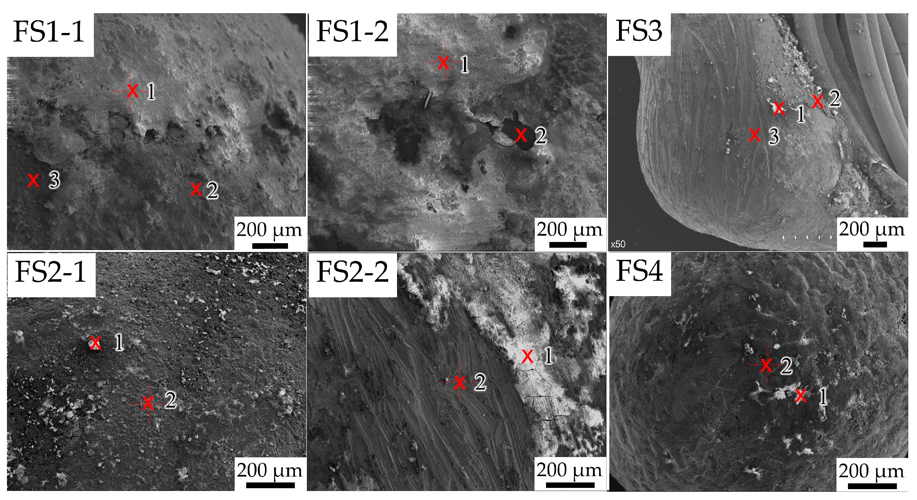
The exterior surface of the samples from real fire scenes was severely damaged and contaminated. It could be caused by fire events or while collecting evidence, as depicted in Figure 2. They were not in an adequate condition to observe the original surface characteristics. Nevertheless, elemental analysis via EDS on the surface is a preliminary examination to determine which elements are contained on the molten mark’s surface, and experimental results might well reveal the source of these samples. EDS analysis was carried out from the molten mark’s outer layer (labeled with 1) to its inner layer (labeled with 2 or 3).
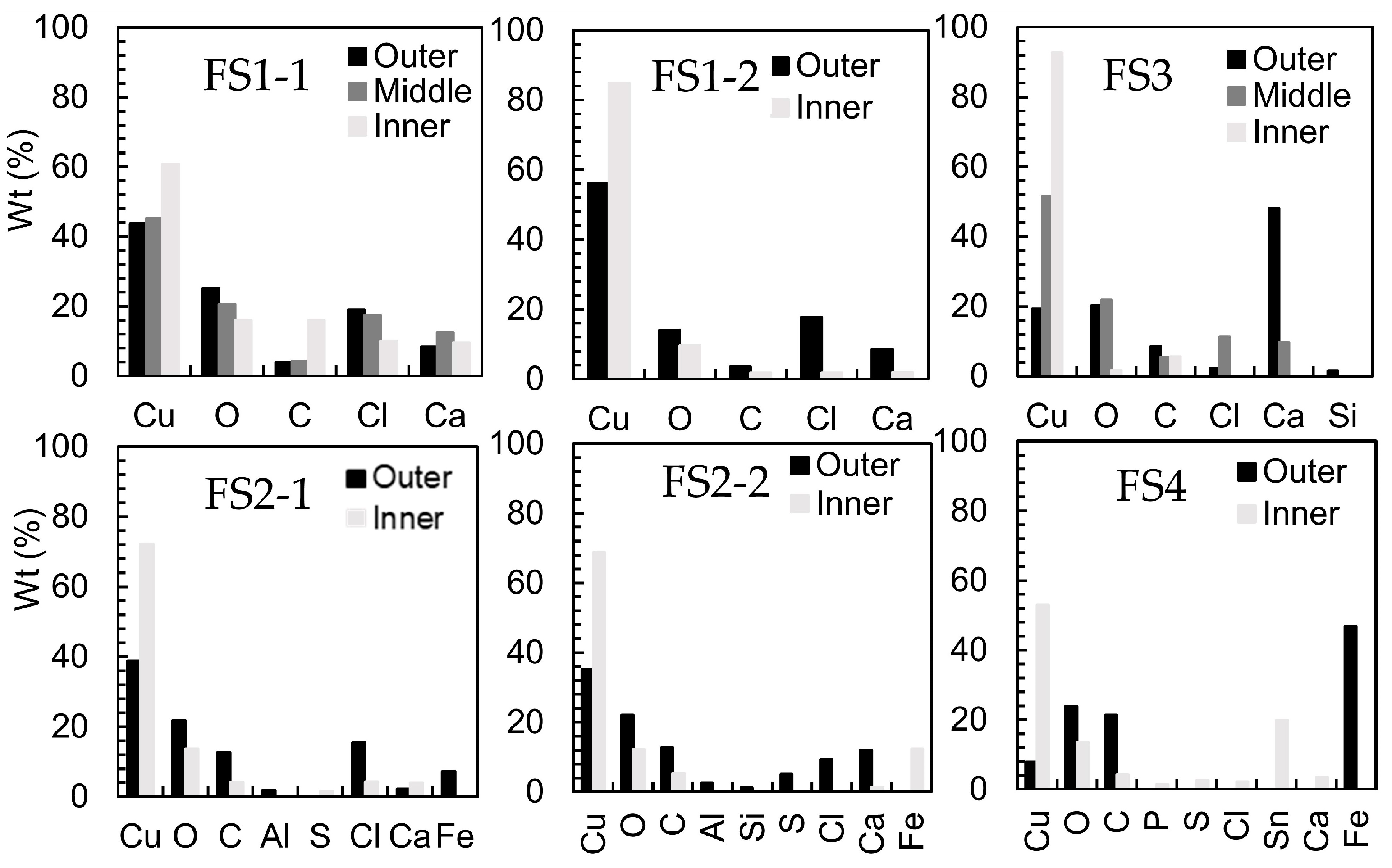
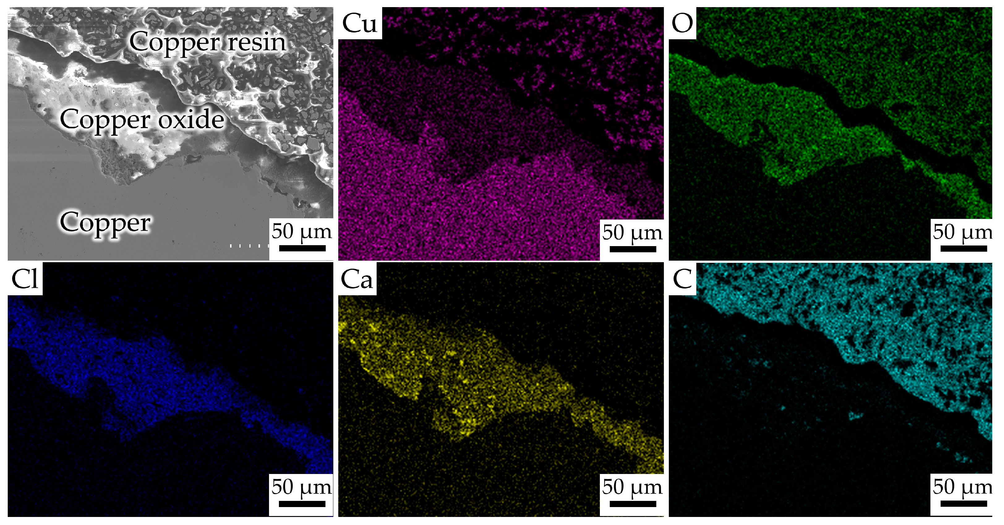
Figure 3 depicts the elemental analysis results on the surface of molten marks from actual fire sites. Copper and oxygen are the two major elements in all molten marks. Oxygen content, in most cases, is clearly the highest at the outer surface and gradually reduces at the inner surface, whereas the reverse applies for copper content. This is the result of oxygen absorption from the surrounding air into the molten mark [5,9]. Carbon, chlorine, and calcium are the minor elements. Figure 4 shows the elemental mapping of Cl and Ca, concentrating on the copper oxide layer. Cl was reported to be emitted from burning PVC insulation, while Ca was released into the atmosphere by ash-forming processes such as wood combustion [14,15,16]. C mostly comes from ambient CO2 during the fire, and the remaining C on the wire’s surface is due to wire combustion [10]. Additionally, several residual elements were detected via EDS on the surface of the molten mark from real fire accidents, including Al, Si, P, Fe, S, and Sn. The residual elements are almost similar in samples collected from the same fire scenes (FS1-1 and FS1-2, and FS2-1 and FS2-2).
In conclusion, the major elements discovered on the surface of the molten mark are Cu and O. C, Cl, and Ca are the minor elements. Depending on their environment, the foreign elements have different elements. Molten marks from the same fires have almost identical foreign elements.

3.3. Microstructural Characterization

The microstructures of all molten marks from real fire sites were analyzed via metallurgical examination. The unetched and etched surfaces were prepared for composition investigation via EDS and microstructure observation, respectively. Figure 5 depicts the microstructural compositions of the unetched molten marks. The following results were observed.
Cases FS1-1 and FS1-2 have comparable compositions because they were obtained from the same fire sites. Case FS2-1 revealed the presence of Cu2O precipitates due to the heat treatment of copper and oxygen in fire and Pb. Pb has been used as a component in electronics [17,18]. In the microstructure, this Pb has a noticeably different metallic color. This could imply that copper wire is directly beneath the material, including Pb, that melted and fell onto the copper wire during a fire and cooling process [15]. On the other hand, case FS2-2, which was collected from the same fire scene as case FS2-1, reveals different alloying elements, including S, but no Cu2O. The two samples could have been gathered from various locations within the same fire scene. The existence of various residual elements in the microstructure could reflect the surrounding materials during molten mark formation. In the case of FS3, the microstructure has no other residual elements. This is identical to the structure of cases FS1-1 and FS1-2. The unetched microstructure of case FS4 is different from those of the others, having Cu in the bright area and Cu + Sn in the dark area. In general, Sn-Pb has been utilized as a solder for connecting electronic components [14,17,19]. Thus, the copper wire with solder may have an alloying area and a rounded end. These effects are caused by the interaction of copper and solder from rapid melting and solidification in the atmosphere [15].
Figure 6 and Figure 7 show the microstructure in the longitudinal section of molten marks on copper wire after etching. The structure of each of the samples differs as follows.
Cases FS1-1, FS1-2, and FS2-2 in Figure 6 show similar equiaxed grain structures as a result of annealing in a firing atmosphere and slowly cooling down [7,8,20,21]. In case FS2-1, oxygen-richer grains are discovered, which may imply a high level of ambient oxygen at the fire site during formation. Interestingly, Figure 7 depicts the microstructure of case FS3, which appears to be a blurred dendrite in a columnar grain. The columnar grain formed in the longitudinal section indicates a rapid heat transfer from one side to the other. This structure indicates a rapidly solidified molten mark. The fire effect causes the blurred dendrite. Because of imperfect dissolution, traces of dendrite still remain in the structure [22,23,24,25]. In addition, small black points within the grain represent gas porosities caused by the dissolution of hydrogen, oxygen, or nitrogen into liquid copper during solidification. Furthermore, the microstructure of case FS4 is unfamiliar, and grain boundaries are not visible. A grain boundary commonly appears after etching with FeCl3 solution if the molten mark contains major elements of copper and oxygen. However, the presence of copper and tin was a major element in this sample, instead of copper and oxygen, and as inspected via EDS, the microstructure of this sample is different from others.

4. Discussion

From examinations, all results were interpreted together to explain the fire environment and the formation of molten marks on copper wire for fire investigation. The discussion of each case is explained as follows.
Cases FS1-1 and FS1-2 exhibit the same grain structure and composition, as depicted in Figure 5, Figure 6 and Figure 7, because they were collected from the same fire scene. The presence of a grain structure indicates that these two molten marks were melted above the melting point and solidified.
For cases FS2-1 and FS2-2, although these two samples were gathered from the same field, the typical microstructure is entirely different. FS2-1 contains oxygen-rich grains, implying that it was melted above the melting temperature in a powerful oxygen environment and slowly solidified. On the other hand, FS2-2 has no oxygen-rich grains, but the residual element S was found in the microstructure in addition to Pb, as illustrated in Figure 5. It was claimed that they were obtained from different surrounding areas but from the same fire scene. Moreover, the presence of residual elements implies that the fire accident occurred before these molten marks were generated on copper, then the surrounding materials were melted and dropped onto that copper wire. Thus, this molten mark was not caused by the fire accident [15].
In case FS3, there is a localized point of contact between two copper conductors, as pointed out by the arrow in Figure 1. The exterior of this molten mark exhibits sharp demarcation between the melted and unmelted areas of the conductor and a round shape. These features are normally exhibited for electrical arc-damaged conductors, as reported by NFPA 921 [15]. In the overview photographs, columnar grains can be seen developing from one side to the other due to rapid solidification. The microstructures at high magnification exhibit blurred copper dendrites inside the columnar grains. The copper dendrites are hardly noticeable because the sample was exposed to fire. From the definition of PMMs by Lee et al. [2,4,6], PMMs are generated at room temperature and rapidly cooled to room temperature before a fire that is located at the fire origin. As a result, this sample has columnar grains growing from one side to the other. Therefore, it is likely to be a PMM formed at the fire origin.
In case FS4, the microstructure of the sample differs from those of the others, which are primarily composed of Cu and Cu + Sn. In general, Sn has been used as a solder composition for joining two electronic components [18,19]. Consequently, Cu and Sn might be melted during metal connection. Nevertheless, the external morphology is rounded, similar to case FS3, and if the external morphology is examined only visually, without a microstructure examination, the judgment of that damage may be inaccurate. Thus, metallurgical examination under the longitudinal section of molten marks on copper wire from real-world fire scenes is necessary for fire investigation.
Therefore, this work was presented as a foundation on which other researchers and fire investigators can investigate fires in different settings. The microstructure as well as the presence (or absence) of residual elements might be useful as guides for fire investigators in explaining and understanding the formation of molten marks and the fire environment. However, a shortcoming of this research is that it is not possible to compare the microstructures with those of other studies because there are no prior works that utilized samples from real-world fire scenes. In the future, it is expected that similar research will be presented and compared to what is presented in this paper.

5. Conclusions

The surface morphology and microstructure of molten marks on copper wire were examined to describe the formation of molten marks on copper wire collected from real fire scenes as well as to identify the surrounding materials. The results provide valuable fire investigation information for the following:
  • The major elements discovered on the surface of molten marks are Cu and O. C, Cl, and Ca are the minor elements. Depending on their environment, the foreign elements have different elements.
  • The surrounding materials during molten mark formation can be evaluated using elemental analysis via EDS of the polished sample without etching.
  • The formation of molten marks on copper wire can be described through microstructural observation in the longitudinal section of the polished sample with etching.
Because of the identical typical appearance on the outer surface, if the external morphology is examined only visually, without a microstructure examination, the judgment of that damage may be inaccurate. Thus, metallurgical examination under the longitudinal section of molten marks on copper wire from real-world fire scenes is necessary for fire investigation.

Author Contributions

Conceptualization, S.S. and H.M.; methodology, S.S. and H.M.; software, S.S., K.M. and H.M.; validation, S.S.; formal analysis, S.S.; investigation, S.S.; resources, H.M. and K.M.; data curation, S.S.; writing—original draft preparation, S.S.; writing—review and editing, S.S. and H.M.; visualization, K.M. and H.M.; supervision, K.M. and H.M. All authors have read and agreed to the published version of the manuscript.

Funding

This research was funded from The Royal Thai Government scholarship.

Institutional Review Board Statement

Not applicable.

Informed Consent Statement

Not applicable.

Data Availability Statement

Not applicable.

Conflicts of Interest

The authors declare no conflict of interest.

References

  1. Wang, Y.; Su, X. Study on Pores Distribution Laws in Secondary Short Circuited Melted Beads of Copper Wires. Procedia Eng. 2014, 84, 887–892. [Google Scholar] [CrossRef] [Green Version]
  2. Lee, E.P.; Ohtani, H.; Matsubara, Y.; Seki, T.; Hasegawa, H.; Imada, S.; Yashiro, I. Study on Discrimination between Primary and Secondary Molten Marks Using Carbonized Residue. Fire Saf. J. 2002, 37, 353–368. [Google Scholar] [CrossRef]
  3. Liu, K.H.; Shih, Y.H.; Chen, G.J.; Chou, J.M. Microstructural Study on Molten Marks of Fire-Causing Copper Wires. Materials 2015, 8, 3776–3790. [Google Scholar] [CrossRef] [Green Version]
  4. Lee, E.P.; Ohtani, H.; Seki, T.; Hasegawa, H.; Imada, S.; Yashiro, I. Study on Discrimination between Primary and Secondary Molten Marks by DAS. Bull. Japan Assoc. Fire Sci. Eng. 2000, 50, 1–12. [Google Scholar]
  5. Liu, K.H.; Shih, Y.H.; Chen, G.J.; Chou, J.M. Microstructural Study on Oxygen Permeated Arc Beads. J. Nanomater. 2015, 2015, 373861. [Google Scholar] [CrossRef] [Green Version]
  6. Lee, E.P.; Ohtani, H.; Seki, T.; Hasegawa, H.; Imada, S.; Yashiro, I. A Fundamental Study on Electrical Molten Marks. Bull. Japan Assoc. Fire Sci. Eng. 2001, 51, 1–10. [Google Scholar] [CrossRef]
  7. Wei, M.M.; Zhao, Z.; Liang, D. Experiment of Electrical Fire Burned Copper Wire and Parameters Analysis on Metallographic Test of Melted Mark. Procedia Eng. 2011, 11, 496–503. [Google Scholar] [CrossRef] [Green Version]
  8. Wei, M.M.; Mo, S.J.; Liang, D.; Li, J.B. The Experiment on Melted Mark Formed by Copper Wire in Electrical Fire and the Analytic Researcher on the Feature Parameters of Metallographic Structure. Procedia Eng. 2011, 11, 504–513. [Google Scholar] [CrossRef] [Green Version]
  9. Babrauskas, V. Arc Beads from Fires: Can “cause” Beads Be Distinguished from “Victim” Beads by Physical or Chemical Testing? J. Fire Prot. Eng. 2004, 14, 125–147. [Google Scholar] [CrossRef]
  10. Wu, Y.; Zhao, C.Z.; Di, M.; Gao, W. The Surface Analysis of Melted Arc Copper Beads. Mater. Sci. Forum 2007, 561, 2455–2458. [Google Scholar] [CrossRef]
  11. Rawdon, H.S.; Lorentz, M.G. Metallographic Etching Reagents for Copper. Sci. Papres Bur. Stand. 1920, 16, 641–668. [Google Scholar] [CrossRef]
  12. Oetzow, G. Metallographic Etching, 2nd ed.; ASM International: Materials Park, OH, USA, 1999; p. 88. [Google Scholar]
  13. Scott, D.A. Metallography and Microstructure of Ancient and Historic Metals; Getty Conservation Institute Publications: Los Angeles, CA, USA, 1991; p. 72. [Google Scholar]
  14. Gramatyka, P.; Nowosielski, R.; Sakiewicz, P. WEEE Recycling of Waste Electrical and Electronic Equipment. J. Achiev. Mater. Manuf. Eng. 2020, 20, 535–538. [Google Scholar]
  15. NFPA 921. Guide for Fire and Explosion Investigations; National Fire Protection Association: Quincy, MA, USA, 2017; pp. 119–135. [Google Scholar]
  16. de Carvalho, A.V. Effects of Potassium and Calcium on the Combustion Behaviour of Biomass. Master’s Thesis, University of Lisbon, Lisboa, Portugal, July 2017. [Google Scholar]
  17. Properties of Solders—2019, Farnell. Available online: https://www.farnell.com/datasheets/315929.pdf (accessed on 31 October 2022).
  18. Howell, K.; Sweatman, K.; Miyaoka, M.; Nishimura, T.; Tran, X.Q.; Mcdonald, S.; Nogita, K. Microalloyed Sn-Cu Pb-Free Solder for High Temperature Applications. In Proceedings of the Surface Mount Technology Association (SMTA), Fort Worth, TX, USA, 13–17 October 2013; SMTA: Eden Prairie, MN, USA, 2013. [Google Scholar]
  19. Mohd, N.M.; Bukhari, M.Z.; Noor, N.A.M.; Jamaludin, S.B. Effect of Temperature to the Microstructure of Sn-Pb Solder Alloy. In Proceedings of the National Metallurgical Conference, Kangar, Malaysia, 9–10 December 2006. [Google Scholar] [CrossRef]
  20. Michael, A.; Hugh, S.; David, C. Materials Engineering, Science, Processing and Design; Butterworth-Heinemann Elsevier Ltd.: Oxford, UK, 2007; pp. 390–392. [Google Scholar]
  21. Kurz, W.; Fisher, D.J. Fundamentals of Solidification, 3rd ed.; Trans Tech Publications Ltd.: Stafa-Zurich, Switzerland, 1989; p. 86. [Google Scholar]
  22. Qin, S.; Bendo, A.; Tsuchiya, T.; Lee, S.; Zou, Y.; Matsuda, K. Effect of Cooling Rate on Precipitation during Homogenization Cooling in Balanced AlMg2Si Alloy. Mater. Trans. 2020, 61, 2115–2120. [Google Scholar] [CrossRef]
  23. Flemings, M.C. Coarsening in Solidification Processing. Mater. Trans. 2005, 46, 895–900. [Google Scholar] [CrossRef] [Green Version]
  24. Glicksman, M.E.; Voorhees, P.W. Ostwald Ripening and Relaxation in Dendritic Structures. Metall. Trans. A Phys. Metall. Mater. Sci. 1984, 15, 995–1001. [Google Scholar] [CrossRef]
  25. William, D.; Callister, J.; Rethwisch, D.G. Fundamentals of Materials Science and Engineering; John Wiley & Sons, Inc.: Hoboken, NJ, USA, 2012; pp. 459–466. [Google Scholar]
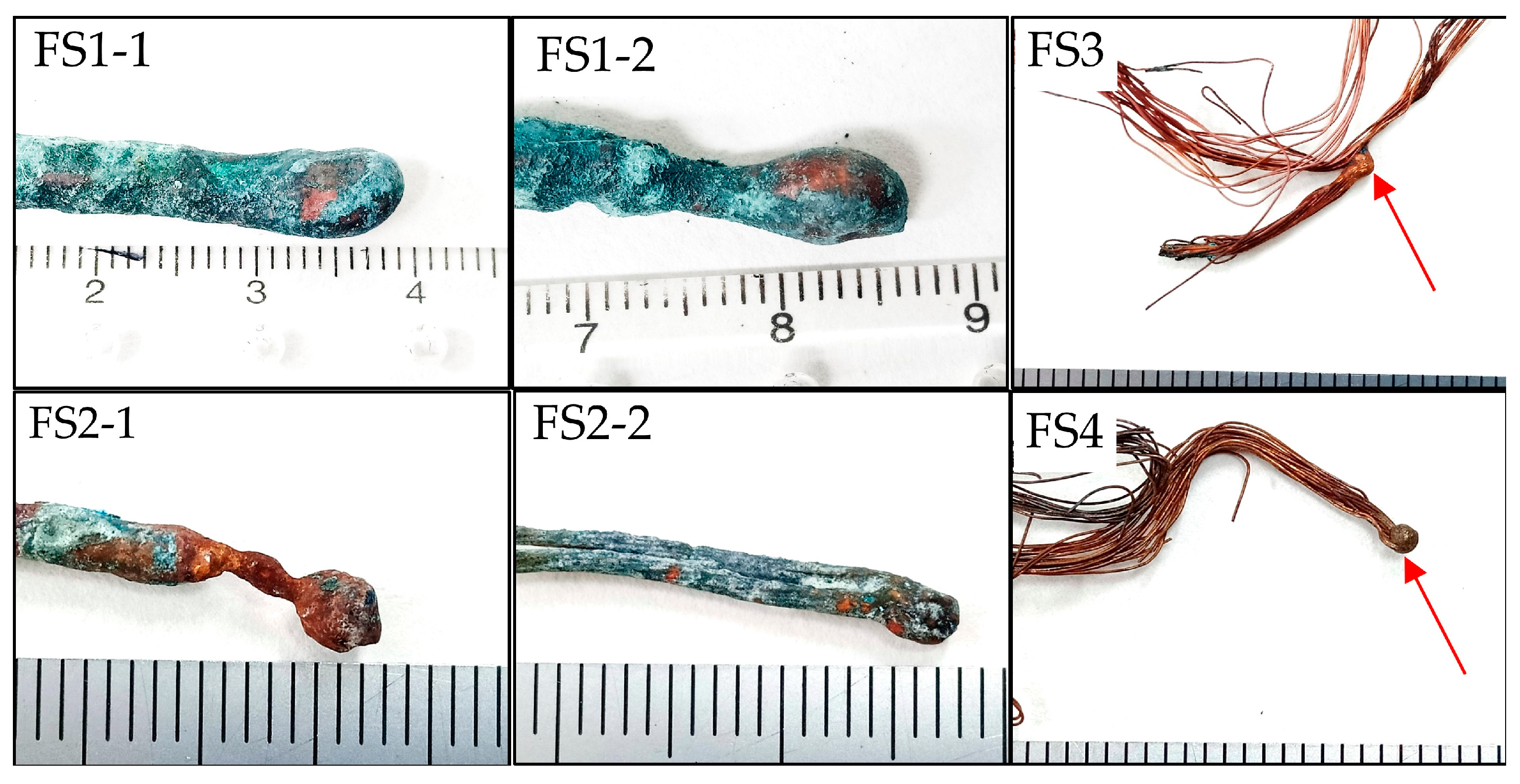
Figure 1. The molten marks on copper wires collected from real-world fire scenes.
Forensicsci 03 00002 g001
Figure 2. Surface morphology of the molten marks on copper wire.
Forensicsci 03 00002 g002
Figure 3. Elemental analysis via EDS on the surface of molten marks.
Forensicsci 03 00002 g003
Figure 4. Elemental mapping on the longitudinal section of the molten mark in case FS1-1.
Forensicsci 03 00002 g004
Figure 5. Microstructural compositions of the molten marks.
Forensicsci 03 00002 g005
Figure 6. Etched microstructure of the molten marks (overview).
Forensicsci 03 00002 g006
Figure 7. Etched microstructure of the molten marks under magnification 200×.
Forensicsci 03 00002 g007
Table 1. Specification of the fire scene samples.
Fire Scene NumberWire TypeWire Diameter (mm)
FS1-1stranded wire4.65
FS1-2stranded wire4.65
FS2-1single1.7
FS2-2stranded wire1
FS3stranded wire1
FS4stranded wire1
Disclaimer/Publisher’s Note: The statements, opinions and data contained in all publications are solely those of the individual author(s) and contributor(s) and not of MDPI and/or the editor(s). MDPI and/or the editor(s) disclaim responsibility for any injury to people or property resulting from any ideas, methods, instructions or products referred to in the content.