Article

Effect of Textured Glasses on Conversion Efficiency in Dye-Sensitized Solar Cells

Graduate School of Engineering, Nagoya University, Nagoya 464-8603, Japan
*
Author to whom correspondence should be addressed.
Nanomanufacturing 2023, 3(3), 315-325; https://doi.org/10.3390/nanomanufacturing3030020
Submission received: 28 April 2023 / Revised: 20 May 2023 / Accepted: 3 July 2023 / Published: 5 July 2023

Abstract

:
In this paper, three types of optical textured glass substrates were prepared at the glass/transparent conductive oxide interface using polydimethylsiloxane nanoimprint lithography to increase the conversion efficiency of dye-sensitized solar cells (DSSCs). There were three types of textures: nanotexture, microtexture, and micro/nano double texture. In terms of optical characteristics, it was confirmed that the reflectance of all of the textured glass substrates was lower than that of flat glass in the mean value of the 400–800 nm wavelength band. Further, the diffuse transmittance was higher than that of flat glass for all of the textured glass substrates, and the D-Tx was particularly high. DSSCs were fabricated using N749 and N719 dyes; their size was 6 mm2. The conversion efficiencies of the N749 DSSCs were improved by 11% for the N-Tx (η of 2.41%) and 10% for the D-Tx (η of 2.38%) compared with flat glass (η of 2.17%) DSSCs. On the other hand, the M-Tx did not improve it. The conversion efficiencies of the N719 DSSCs with textured glass substrates were improved by 7.5% for the M-Tx (η of 2.74%), 18% for the N-Tx (η of 3.01%), and 26% for the D-Tx (η of 3.22%) compared with flat glass (η of 2.55%) DSSCs.

1. Introduction

Nowadays, the contribution of installed photovoltaics to the global electricity demand has been accelerating and reached more than 2.7% in 2020. This trend is expected to continue growing [1]. Dye-sensitized solar cells (DSSCs) have a simple structure and have attracted attention owing to their relatively low material cost compared with various other photovoltaic solar cells [2,3,4,5,6]. DSSCs are solar cells that excite dye and extract electrons from them and generate electricity so they can use only dye-absorbable wavelengths, whereas Si photovoltaics use almost all visible wavelengths. Another characteristic of DSSCs not found in other solar cells is that DSSCs have various colors. It is because they tend to absorb certain wavelengths in visible light. Thus, they are beautiful like stained glasses, which collect some of the wavelengths and allow the others to pass through.
Figure 1 shows schematics of (A) the conventional and (B) the proposed DSSCs. For photoexcitation, the titanium dioxide (TiO2) light absorption layer [7], which has a bandgap of 3.2 eV [8], must be irradiated by light with a wavelength of 390 nm or less. However, in the spectral distribution of sunlight, the wavelengths below 390 nm are few in terms of total energy [9]. Therefore, to use light in the visible wavelength, which is the main wavelength of sunlight, TiO2 is colored with dye that absorbs visible light and sensitizes the layer. A colored solar cell can be manufactured by arbitrarily selecting a dye, and DSSCs are expected to be used differently from other solar cells. However, the conversion efficiency of DSSCs (11.9 ± 0.4%) is lower than that of other solar cells such as ordinary silicon-based crystalline solar cells (26.7 ± 0.5%), perovskite solar cells (22.6 ± 0.6%), and CIGS solar cells (23.35 ± 0.5%) [10].
The conversion efficiency of DSSCs was improved by the optical and electrical characteristics of the front and back glass. Typical approaches of optical engineering include optical management to increase the light utilization rate. Light management includes roles such as antireflection (AR) [11,12,13,14], light trapping (LT) [15,16], and light scattering (LS) [17,18]. One of the electrical approaches is a way to change the counter electrode at a back glass of DSSCs from Pt to a better catalyst, such as FeS2 [19]. Another approach for electrical properties is to introduce a block layer such as a TiO2/ZnO bilayer to interfere with the recombination at the electrode/nanoparticle interface [20].
Antireflection techniques are classified as either antireflection coating (ARC) [11,12] or antireflection texture (ART) [13,14]. In an ARC, the change in the refractive index at the interface can be moderated by coating the sun-facing glass with a material that has an intermediate refractive index and an appropriate thickness, which reduces reflection. On the other hand, in an ART, the average refractive index can be made gentle by forming a microstructure in the subwavelength order at the interface, which also reduces reflection. In general, reflection occurs at the air/glass substrate interface, so the sun-facing glass in all photovoltaic solar cells is treated with an ARC or ART. We defined these AR techniques as outer AR.
Furthermore, in thin-film solar cells fabricated on a glass substrate with transparent conductive oxide (TCO), AR techniques that are applied to the bottom side of the front glass (i.e., the inner surface of the solar cell on the power generation layer side) is defined as inner AR. In thin-film solar cells such as thin-film Si solar cells and DSSCs, reflection also occurs at the interface between the glass/TCO layer and the TCO absorption layer. To reduce this reflection, inner AR techniques are adopted. These techniques are classified as either inner ARC or inner ART. In principle, outer AR is superior to inner AR, so it has many applications. However, because outer AR is formed on the outer surface of the solar cell, it tends to deteriorate over time owing to external factors [21,22]. On the other hand, inner AR is protected inside the solar cell, so long-term effects can be expected. In particular, the function of inner ART can also include LT or LS. It is possible to trap part of the incident light and increase the optical path length in the light absorption layer. The glass substrates that have these functions are called textured glasses.
Previous research [2] (see Figure 1B) fabricated a nano-order dimple texture (N-Tx) and a micro/nano-order double dimple texture (D-Tx) made from SiO2 at the glass/TCO interface as LS and inner ART. The study confirmed that the utilization rate of light improved owing to the LS and AR effects and that the conversion efficiency of the DSSCs was also improved. Dyes for DSSCs have various colors and absorption wavelengths. Therefore, in this paper, we created a new M-Tx with microdimples for the simple purpose of increasing the diffuse transmittance. DSSCs using two dyes were fabricated on three types of textured glass. We also investigated the relationship between the textured glasses and the dye.

2. Methods

2.1. Master and Replica Molds Preparation

In the previous research, we fabricated DSSCs (N749 dye) using N-Tx- and D-Tx-textured glasses, and both cells had improved conversion efficiencies. However, the improved performance parameters of both cells were very different. It was thought that these differences were caused by the optical and ohmic characteristics of the textured glass with fluorine-doped tin oxide (FTO). Therefore, in this study, we created a microtexture (M-Tx) with the simple aim of increasing the diffuse transmittance. This microdimple structure was the same as that of a D-Tx.
M-Tx was prepared by one-time anodizing and wet etching. First, a pretreated 1 mm thick Al sheet was electropolished [23]. Then, the Al sheet was anodized at 185 V in a 1:4 v/v solution of ethanol (C2H5OH) and 1 wt.% phosphoric acid (H3PO4), which was stirred at 600 rpm. The solution temperature at that time was in the range of 0 °C–15 °C, and the anodization was carried out for 45 min. Finally, wet etching was performed with 6 wt.% H3PO4 at room temperature for 11 h. This M-Tx mold was anodized again to become the master mold of D-Tx [2].
Before making a replica of the polydimethylsiloxane (PDMS) mold, the master mold was coated with a release agent (OPTOOL HD 2100, Daikin Co., Ltd., Osaka, Japan). A hard PDMS (X-32-3095, Shin-Etsu Chemical Co., Ltd., Tokyo, Japan) was used for the replica molds. We poured an appropriate amount of PDMS onto the master mold and performed vacuum defoaming of the PDMS for 30 min. After defoaming, the PDMS was cured by heating on a hot plate at 150 °C for 30 min. The size of the replica mold was made to be slightly smaller (approximately 18–19 mm2) than the glass substrate (20 mm2) for easy imprinting.

2.2. PDMS Nanoimprinting Process

Figure 2 shows the process of fabricating the textured glass. The conditions are shown in Table 1. We used both the master and replica molds made in the previous research. Borosilicate glass (Eagle XG, Corning Inc., New York, NY, USA) was used as the substrate, and the size was 20 mm × 20 mm × 0.4 mm. The textures were formed on the substrate by PDMS NIL at room temperature using an organosilsesquioxane (OSQ, TOKYO OHKA KOGYO CO. Ltd. Kawasaki, Japan) solution under a pressure of about 0.1 MPa (Figure 2(1),(2)). The PDMS mold and substrate were kept pressed for several hours to absorb the solvent (Figure 2(3)). After demolding (Figure 2(4)), the imprinted glass substrates were baked in the air (Figure 2(5)). The baking conditions were 150 °C for 60 min, 250 °C for 30 min, and 480 °C for 30 min, continuously. During the baking, the OSQ became SiO2, which had the same optical properties as the glass substrate.

2.3. Fabrication of DSSCs

TCO film was prepared on the textured substrate to impart conductivity. An FTO film was formed as a TCO film. The FTO film was deposited to a thickness of 700–800 nm using the spray pyrolysis deposition (SPD) method at SPD Laboratory, Inc. The FTO has a resistance of approximately 9.3 Ω/sq on a flat substrate and a refractive index of about 2.006. Next, a TiO2 electrode was prepared on textured glass with FTO.
Using the screen-printing method, using a desktop hand rubbing table for screen printing (“WHT-LAB”, MINO GROUP Co., Ltd., Gujo, Japan) and a screen mask (screen mask, Mitani Micronics Co., Tama, Japan), paste-like TiO2 with 15 to 20 nm diameter nanoparticles was coated onto the glass substrates and baked at 120 °C for 30 min and at 480 °C for 30 min, with a heating rate of 20 °C/min, continuously with an electric muffle furnace (small programmable electric furnace, AS ONE Co., Osaka, Japan). After baking, the substrate with TiO2 was cooled as well as the furnace. The thickness of the TiO2 electrode after heating was about 4.5 µm. We also prepared a flat TiO2 electrode (TiO2 electrode on flat glass) as a reference.
Then, the substrates were immersed in N719 dye (cis-diisothiocyanato-bis(2,2′-bipyridyl-4,4′-dicarboxylato) ruthenium (II) bis(tetrabutylammonium), Solaronix SA) solution for 24 h. Following their removal from the dye solution, the substrates were rinsed with ethanol and manually sealed with a hot melt film (Meltonix 1170-60, Solaronix SA) at a temperature of 110 °C using a platinum electrode. Finally, an electrolyte (Iodolyte HI-30, Solaronix SA) was filled between the TiO2 and platinum electrode, and the electrolyte spout was closed with a seal. This produced DSSCs with an active area of 0.36 cm2 (0.6 cm × 0.6 cm).

3. Results

3.1. Textured Glass Substrates

Figure 3 shows an SEM image of the produced M-Tx master mold. Surface observations were performed using SEM (Miniscope® TM3030, Hitachi High-Tech Corp.Tokyo, Japan). The dimple diameter was about 1–3 µm, and the depth was about 0.5–1.0 µm; therefore, we succeeded in producing the target texture.
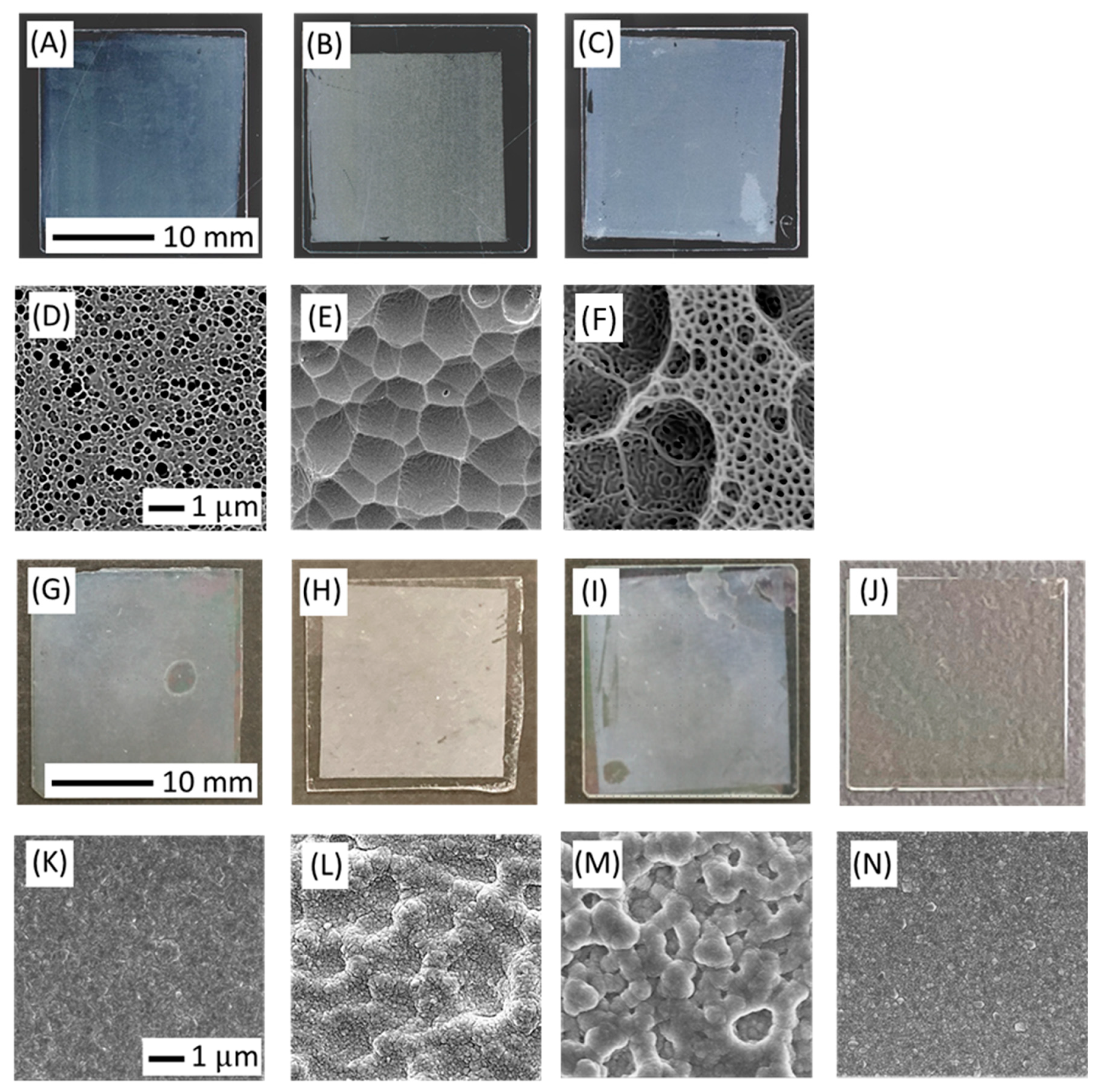
Figure 4 shows optical and SEM images of the three types of textured glass, with and without FTO. The optical images were made using an optical microscope (VHX-2000, Keyence Corp., Osaka, Japan), and the SEM images were made using a field emission scanning electron microscope (FE-SEM, JSM-7500FA, JEOL Ltd., Tokyo, Japan). The surface of each textured glass with FTO became white, like frosted glass, and it could be seen that the light was scattered. The optical properties of each textured glass are shown in the optical properties section.
Figure 4D–F shows the SEM images of the textured glass substrates. In Figure 4D, the N-Tx had nano-size dimples with a diameter of about 200–400 nm and a depth of about 200–400 nm. In Figure 4E, the M-Tx had micro-size dimples with a diameter of about 1–3 µm and a depth of 0.5–1.0 µm. This structure was similar to that of the master mold, as shown in Figure 3, and the master mold could be well replicated. The SEM image of the D-Tx in Figure 4F shows double dimples. The micro-size dimples had a diameter of about 1–3 µm and a depth of 0.5–1.0 µm. The nano-size dimples had a diameter of about 200–400 nm and a depth of about 200–400 nm. It was confirmed that the structures of the N-Tx and D-Tx were the same as those in the previous work [2].
Figure 4K–N shows the SEM images of textured and flat glass substrates with FTO. As shown in Figure 4N, in the surface morphology of FTO on the flat glass fabricated by SPD, there is a fine texture that consists of nanoparticles with a diameter of about several 10–100 nm. As shown in Figure 4K, such a fine texture was also formed in the N-Tx but the texture seen in the imprinted substrate disappeared. Probably, the texture could not be maintained because the nanodimpling was buried during the FTO film formation and the film was formed on top of it.
In Figure 4L, the FTO on the M-Tx shows dimples with a diameter of about 1–3 µm, which is close to the original texture. However, it is believed that there were spherical micro-size bumps at the edge of the microdimpling on the textured glass. Moreover, a fine texture was also formed in the M-Tx. In Figure 4M, the FTO structure consists of spherical micro-size bumps, similar to those in the M-Tx. However, unlike the M-Tx, the FTO did not form a fine texture.
Figure 5 shows the SEM images of the cross-sectional shapes of the textured and flat glass substrates with FTO. Although the surfaces show original nano-size textures from the FTO deposited by SPD, the morphologies of the FTO on flat glass (Figure 5A) and N-Tx (Figure 5B) had nearly flat and uniform thicknesses. This indicates that the texture was buried by the FTO on the N-Tx. On the other hand, it was observed that the FTO film was greatly undulated on both the M-Tx (Figure 5C) and D-Tx (Figure 5D). These results seem to have been largely caused by the microdimples in the texture. However, the morphology of the FTO on the M-Tx is different from the textured glass. With the SPD method, more FTO precursors tended to be deposited at the edge of the dimple structure because of the wettability effect of the FTO precursor. Then, the shape of the FTO at the edge of the micro-size dimple structure became rounded, as shown in Figure 4L,M.

3.2. Optical Properties

The optical properties of the textured glass substrates with FTO were measured using a UV/vis spectrophotometer equipped with an integrating sphere system (V-570, JASCO Corp., Hachioji, Japan). For optical characteristics evaluation, the transmittance and reflectance were measured and evaluated.
Figure 6 shows the optical properties of each textured substrate. Regarding the diffuse transmittance (Figure 6A), its mean value in the 400–800 nm wavelength band was 17.8% for the M-Tx, 5.8% for the N-Tx, and 43.3% for the D-Tx. The diffuse transmittance of the D-Tx was the highest. It was shown that the nanotexture had a weak diffusion effect and that of the microtexture was strong. However, the D-Tx, which combined micro and nanotextures, could obtain an even greater diffuse effect. It is assumed that this was because the wavelength bands of light diffused by the microtexture and nanotexture were different and a complicated diffuse effect was produced within the D-Tx.
Regarding reflectance (Figure 6B), the mean value of the total reflectance in the wavelength band of 400–800 nm was 7.9% for flat glass without a texture. Meanwhile, it was 6.7% for the M-Tx, 6.4% for the N-Tx, and 7.2% for the D-Tx. The reflectance of the textured glass substrates was about 1% lower than that of flat glass. These results indicate the two effects of texture. One is the effect of the ARC. The refractive index of the textured SiO2 was about 1.41, which was lower than that of the glass substrate at about 1.5. Therefore, the reflectance of the M-Tx and D-Tx was reduced by the ARC effect. In addition, it is believed that the N-Tx had an ART effect and showed the lowest reflectance. Therefore, the total transmittance (Figure 6A) was significantly different between textures for the same reason as reflectance.
Figure 7 shows the optical characteristics of the textured substrate with FTO. In terms of total transmittance (Figure 7A), the D-Tx clearly had a lower total transmittance than the other textures. This was due to the increased absorption in the FTO layer caused by the effect of LS. It is speculated that the light scattered by the texture increased the optical path length in the FTO layer, owing to the spherical formation of FTO, and was absorbed by the FTO. Similarly, an increase in the optical path length in the TiO2 layer, which is a light absorption layer, could be expected. In terms of diffuse transmittance (Figure 7B), its mean value in the wavelength band of 400–800 nm was 1.8% for flat glass, 41.1% for the M-Tx, 7.2% for the N-Tx, and 38.5% for the D-Tx. Compared with the textured glass substrates, it increased in the M-Tx and N-Tx but decreased in the D-Tx. These results are also considered to be caused by the formation of FTO film. For the M-Tx and N-Tx, the FTO had a fine texture. It is believed that this fine FTO texture produced a further diffuse effect. On the other hand, in the D-Tx, it is suggested that the coarsening of the FTO did not produce a further LS effect and reduced the diffuse effect originally seen in the texture without FTO.
In terms of reflectance (Figure 7B), the formation of FTO causes light interference, and the graph is a waveform. The mean value of reflectance in the wavelength band of 400–800 nm was 11.1% for flat glass, 13.3% for the M-Tx, 10.6% for the N-Tx, and 14.2% for the D-Tx. All these substrates had higher reflectance than the textured substrate without FTO. These results were caused by the high reflectance at the interface between the FTO and air, which had a large difference in the refractive index. In the actual DSSCs structure, because the FTO was coated with TiO2, high reflectance at FTO/air interface was not observed.

3.3. Characteristics of DSSCs

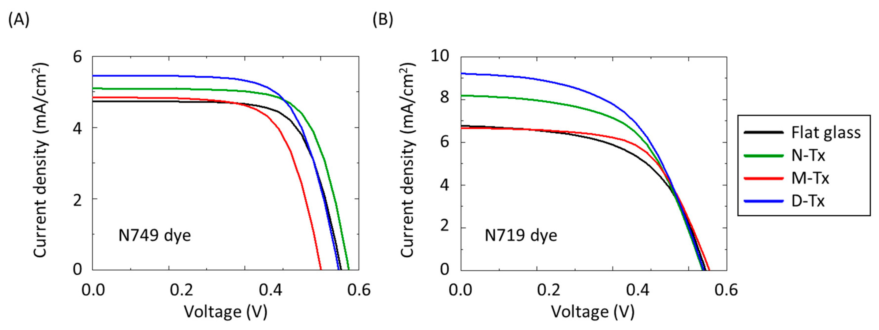
Figure 8 shows the I–V curves of the DSSCs with the (A) N749 and (B) N719 dyes. Table 1 shows a summary of the DSSCs’ performances. These evaluations were measured using a solar simulator (XES-155S1, SAN-EI ELECTRIC Co., Ltd., Tokyo, Japan) under standard test conditions (AM1.5G, 1SUN (100 mW/cm2), 25 °C). The experiment temperature was kept constant by taking time between every measurement to appropriately cool the measurement device and samples because the conversion efficiency of DSSCs is affected by the temperature. The performances of DSSCs with textured glass substrates were compared with those that had flat glass. In Table 2, the rate of change of each dye from flat glass is shown below each characteristic value, such as conversion efficiency (η), short-circuit current density (Jsc), open-circuit voltage (Voc), and fill factor (FF). However, the absolute values cannot be simply compared between N749 and N719 because the absolute performance, such as the best conversion efficiency, is different.
In the case of N749, as shown in Figure 8A, the performance parameters of flat glass were a Jsc of 4.75 mA/cm2, Voc of 0.65 V, FF of 0.70, and η of 2.17%. The Jsc of the N-Tx increased to 5.11 mA/cm2 (rate of change was 8%). Moreover, the Voc and FF of N-Tx remained near value. In addition, the η of the N-Tx improved and was 2.41%. Meanwhile, the Jsc of D-Tx increased to 5.48 mA/cm2 (rate of change was 15%), which was higher than that of the N-Tx, and its Voc remained nearly in value. In addition, the η of D-Tx had improved and was 2.38%. The performance parameters, except for Jsc, decreased, so the M-Tx did not improve cell performance. The tendencies of the cell performances of the N-Tx and D-Tx were similar to the results of previous works [2]. Therefore, in the DSSCs with N749 dye, the N-Tx had the most improved conversion efficiency.
In the case of N719, as shown in Figure 8B, the performance parameters of flat glass were a Jsc of 6.83 mA/cm2, Voc of 0.65 V, FF of 0.57, and η of 2.55%. The Jsc of the N-Tx increased to 8.19 mA/cm2 (rate of change was 20%). In addition, the Voc and FF of the N-Tx remained near value. In addition, the η of N-Tx improved and was 3.01%. Meanwhile, the Jsc of the D-Tx increased to 9.22 mA/cm2 (rate of change was 35%), and its Voc remained near value. Moreover, the η of the D-Tx improved and was 3.22%. In addition, the Jsc and Voc of the M-Tx remained nearly value, and its FF improved to 0.62 (rate of change was 9%). Finally, the η of the D-Tx improved to 2.74%. Therefore, in the DSSCs with N719 dye, the D-Tx had the most improved conversion efficiency. In both dyes’ solar cells, the FF of DSSCs using rough textures (M-Tx, D-Tx) was far from those using flat textures (flat glass, N-Tx). It is suggested that this was caused by variation in resistance across the textured surfaces. In the future, we should focus on the study of not only the optical but also the electrical properties of FTO on the textured substrate.

4. Discussion

It is believed that the effect of a textured structure on cell performance depends on the dye used on the DSSCs. As shown in Figure 4K and Figure 5B, the morphology of the FTO on the N-Tx was that of a fine nanocrystal of uniform thickness because the imprinted simple nanostructure was buried by FTO. However, the results of Figure 6B and Figure 7B indicate that LS occurred and was enhanced by the N-Tx. On the other hand, the effect of textured glass on the Voc is hardly shown in Figure 8. Moreover, it is believed that the ohmic loss between the FTO on the N-Tx and the TiO2 did not change from flat glass; therefore, the FF did not change either. From these results, the N-Tx enhanced the optical light path in the TiO2 absorption layer without degrading the FF. Therefore, the Jsc was enhanced by the N-Tx, and the conversion efficiency of the DSSCs with N749 and N719 dyes on the N-Tx increased.
In the case of the M-Tx, the morphology of the FTO on the M-Tx was a fine nanocrystal with a wavy micro-size surface caused by microdimples. From the results in Figure 6B and Figure 7B, although the M-Tx also had enhanced LS and increased diffuse transmittance, its total transmittance slightly decreased. It was indicated that the light absorption in the FTO layer was low. From the results in Figure 8, Jsc, of the DSSCs with N749 and N719 dyes on the M-Tx were not enhanced, although the M-Tx showed high diffuse transmittance. It was suggested that the LS caused by the M-Tx did not enhance the optical light path in the TiO2 absorption layer. This might have been the effect of the micro/nano structure on the scattering angle. Therefore, the Jsc was not enhanced by the M-Tx and the conversion efficiency of the DSSCs with M-Tx was not improved to the extent we expected.
In the case of the D-Tx, the morphology of FTO on the D-Tx was very complicated and consisted of coarse spherical micro-size FTO particles and nanocrystals on the surface. In addition, there was a bumpy structure caused by microdimples. From the results of Figure 6B and Figure 7B, the D-Tx also had enhanced LS and increased diffuse transmittance by micro- and nano-size textures. In addition, the total transmittance of the D-Tx greatly decreased because light absorption in the FTO layer was high. However, from the results of Figure 8, the Jsc of the DSSCs with N749 and N719 dye on the D-Tx were greatly enhanced, although the amount of light that reached the TiO2 layer was decreased by light absorption in the FTO. In particular, the effect of the D-Tx on the Jsc of the N719 dye was remarkable compared with the N749 dye. It is believed that these results were caused by the absorption wavelength of the dye used [24]. It might also have been caused by the effect of the wavelength on the scattering angle. In addition, it is considered that the ohmic loss between the FTO on the D-Tx and TiO2 was significant; therefore, the FF decreased. However, because the improvement of the Jsc exceeded the degradation of the FF, the D-Tx had the highest conversion efficiency among the N719 dyes. On the other hand, the N-Tx had the highest conversion efficiency among the N749 dyes.
From these results, simply increasing the diffused light did not improve the conversion efficiency regardless of the dye. It was confirmed that the conversion efficiencies of both dyes were significantly improved in the DSSCs with textured substrates (N-Tx, D-Tx) that contained nanotextures. In addition, because the micro/nano double texture (D-Tx) showed an LT effect, it might have been caused by the optimized combination of the double texture with the low degradation of the FF. For the Voc, no significant effect on the textures was observed to be related to the difference in dyes. This suggests that the Voc was unaffected by the dye and texture combination.

5. Conclusions

In summary, we prepared three types of textured glass substrates and applied them to DSSCs using two types of dye (N749 and N719). Compared with flat glass, the N-Tx increased most (11%) with the N749 dye and D-Tx increased most (26%) with the N719 dye in terms of conversion efficiency. On the other hand, although the M-Tx showed the highest diffuse transmittance (41.1%) on the textured substrate with FTO, no significant improvement in conversion efficiency was confirmed for both dyes. Therefore, simply increasing the diffused light did not contribute to an improvement in conversion efficiency regardless of the dye. These results suggest that each dye had a suitable texture, which might be a simple nanostructure or an optimized combination of double texture with low degradation of the FF.

Author Contributions

J.S. proposed the concept, provided overall instructions, and revised this manuscript. R.K. performed experiments and wrote this manuscript. Y.N., S.H. and C.O. gave some advice on the process and experiment. All authors have read and agreed to the published version of the manuscript.

Funding

This research received no external funding.

Data Availability Statement

Not applicable.

Conflicts of Interest

The authors declare no conflict of interest.

References

  1. Jacak, J.; Jacak, W. Routes for Metallization of Perovskite Solar Cells. Materials 2022, 15, 2254. [Google Scholar] [CrossRef] [PubMed]
  2. Yang, N.; Oka, C.; Hata, S.; Sakurai, J. Fabrication of textured substrates for dye-sensitized solar cells using polydimethylsiloxane nanoimprint lithography. Adv. Opt. Technol. 2019, 8, 491. [Google Scholar] [CrossRef]
  3. O’regan, B.; Grätzel, M. A low-cost, high-efficiency solar cell based on dye-sensitized colloidal TiO2 films. Nature 1991, 353, 737. [Google Scholar] [CrossRef]
  4. Hagfeldt, A.; Boschloo, G.; Sun, L.; Kloo, L.; Pettersson, H. Dye-sensitized solar cells. Chem. Rev. 2010, 110, 6595. [Google Scholar] [CrossRef]
  5. Karim, N.A.; Mehmood, U.; Zahid, H.F.; Asif TKarim, N.A.; Mehmood, U.; Zahid, H.F.; Asif, T. Nanostructured photoanode and counter electrode materials for efficient Dye-Sensitized Solar Cells (DSSCs). Sol. Energy 2019, 185, 165. [Google Scholar] [CrossRef]
  6. Gnanasekar, S.; Kollu, P.; Jeong, S.K.; Grace, A.N.; Gnanasekar, S.; Kollu, P.; Jeong, S.K.; Grace, A.N. Pt-free, low-cost and efficient counter electrode with carbon wrapped VO2 (M) nanofiber for dye-sensitized solar cells. Sci. Rep. 2019, 9, 5177. [Google Scholar] [CrossRef] [Green Version]
  7. Yang, X.; Yanagida, M.; Han, L. Reliable evaluation of dye-sensitized solar cells. Energy Environ. Sci. 2013, 6, 54. [Google Scholar] [CrossRef]
  8. Dette, C.; Pérez-Osorio, M.A.; Kley, C.S.; Punke, P.; Patrick, C.E.; Jacobson, P.; Giustino, F.; Jung, S.J.; Kern, K. TiO2 anatase with a bandgap in the visible region. Nano Lett. 2014, 14, 6533. [Google Scholar] [CrossRef]
  9. Griffith, M.J.; Mozer, A.J. Porphyrin Based Dye Sensitized Solar Cells; IntechOpen: London, UK, 2011. [Google Scholar]
  10. Green, M.; Dunlop, E.; Hohl-Ebinger, J.; Yoshita, M.; Kopidakis, N.; Hao, X. Solar cell efficiency tables (version 57). Prog. Photovolt. 2021, 27, 3. [Google Scholar] [CrossRef] [Green Version]
  11. Prado, R.; Beobide, G.; Marcaide, A.; Goikoetxea, J.; Aranzabe, A. Development of multifunctional sol–gel coatings: Anti-reflection coatings with enhanced self-cleaning capacity. Sol. Energy Mater. Sol. Cells 2010, 94, 1081. [Google Scholar] [CrossRef]
  12. Menna, P.; Di Francia, G.; La Ferrara, V. Porous silicon in solar cells: A review and a description of its application as an AR coating. Sol. Energy Mater. Sol. Cells 1995, 37, 13. [Google Scholar] [CrossRef]
  13. Zhang, J.; Shen, S.; Dong, X.X.; Chen, L.S. Low-cost fabrication of large area sub-wavelength anti-reflective structures on polymer film using a soft PUA mold. Opt. Express 2014, 22, 1842. [Google Scholar] [CrossRef] [PubMed]
  14. Tsai, J.K.; Tu, Y.S. Fabrication of polymeric antireflection film manufactured by anodic aluminum oxide template on dye-sensitized solar cells. Materials 2017, 10, 296. [Google Scholar] [CrossRef] [PubMed] [Green Version]
  15. Müller, J.; Rech, B.; Springer, J.; Vanecek, M. TCO and light trapping in silicon thin film solar cells. Sol. Energy 2004, 77, 917. [Google Scholar] [CrossRef]
  16. Winz, K.; Fortmann, C.M.; Eickhoff, T.; Beneking, C.; Wagner, H.; Fujiwara, H.; Shimizu, I. Novel light-trapping schemes involving planar junctions and diffuse rear reflectors for thin-film silicon-based solar cells. Sol. Energy Mater. Sol. Cells 1997, 49, 195. [Google Scholar] [CrossRef]
  17. Mustafa, M.N.; Sumlaimah, Y. Fully flexible dye-sensitized solar cells photoanode modified with titanium dioxide-graphene quantum dot light scattering layer. Sol. Energy 2020, 212, 332. [Google Scholar] [CrossRef]
  18. Tsai, C.-H.; Hsu, S.-Y.; Huang, T.-W.; Tsai, Y.-T.; Chen, Y.-F.; Jhang, Y.; Hsieh, Y.; Wu, C.-C.; Chen, Y.-S.; Chen, C.-W.; et al. Influences of textures in fluorine-doped tin oxide on characteristics of dye-sensitized solar cells. Org. Electronics 2011, 12, 2003. [Google Scholar]
  19. Huang, S.; He, Q.; Chen, W.; Zai, J.; Qiao, Q.; Qian, X. 3D hierarchical FeSe2 microspheres: Controlled synthesis and applications in dye-sensitized solar cells. Nano Energy 2015, 15, 205. [Google Scholar] [CrossRef]
  20. Ahmad, Z. Increasing the efficiency of TiO2-based DSSC by means of a double layer RF-sputtered thin film blocking layer. Optik 2020, 207, 164419. [Google Scholar]
  21. Klimm, E.; Lorenz, T.; Weiss, K.-A. Can Anti-Soiling Coating on Solar Glass Influence the Degree of Performance Loss over Time of PV Modules Drastically? In Proceedings of the 28th EU PVSEC, Paris, France, 30 September–4 October 2013; p. 3099. [Google Scholar]
  22. Midtdal, K.; Jelle, B.P. Self-cleaning glazing products: A state-of-the-art review and future research pathways. Sol. Energy Mater. Sol. Cells 2013, 109, 126. [Google Scholar] [CrossRef] [Green Version]
  23. Wu, J.T.; Chang, W.Y.; Yang, S.Y. Fabrication of a nano/micro hybrid lens using gas-assisted hot embossing with an anodic aluminum oxide (AAO) template. J. Micromech. Microeng. 2010, 20, 075023. [Google Scholar] [CrossRef]
  24. Swati, S.; Mohan, P.; Kumar, V.A.; Prakash, S.S.; Sanjay, T. Enhanced photovoltaic performance via co-sensitization of Ruthenium (II)-based complex sensitizers with metal-free indoline dye in dye-sensitized solar cells. Org. Photonics Photovolt. 2017, 5, 9. [Google Scholar]
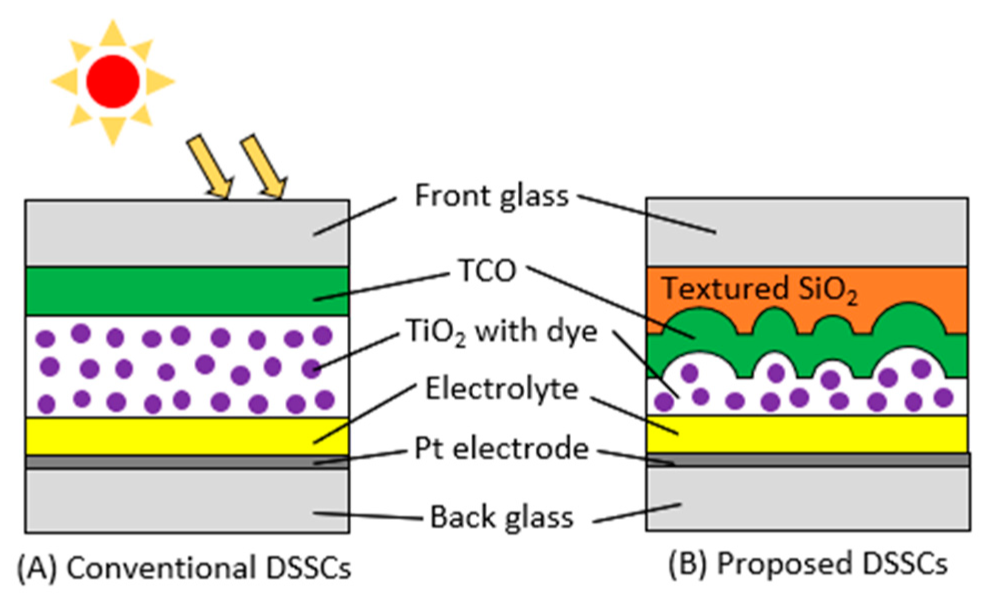
Figure 1. Schematic diagram of DSSCs.
Nanomanufacturing 03 00020 g001
Figure 2. Process of fabricating the textured substrate.
Nanomanufacturing 03 00020 g002
Figure 3. SEM images of M-Tx master mold.
Nanomanufacturing 03 00020 g003
Figure 4. Textured substrates with SEM images: (A) N-Tx, (B) M-Tx, (C) D-Tx, (D) SEM image of N-Tx, (E) SEM image of M-Tx, (F) SEM image of D-Tx, (G) N-Tx with FTO, (H) M-Tx with FTO, (I) D-Tx with FTO, (J) flat glass with FTO, (K) SEM image of N-Tx with FTO, (L) SEM image of M-Tx with FTO, (M) SEM image of D-Tx with FTO, and (N) SEM image of flat glass.
Nanomanufacturing 03 00020 g004
Figure 5. Cross-sectional shape of substrates with FTO: (A) flat glass, (B) N-Tx, (C) M-Tx, and (D) D-Tx.
Nanomanufacturing 03 00020 g005
Figure 6. Optical characteristics of textured substrates: (A) transmittance, (B) reflectance.
Nanomanufacturing 03 00020 g006
Figure 7. Optical characteristics of textured substrates with FTO: (A) transmittance, (B) reflectance.
Nanomanufacturing 03 00020 g007
Figure 8. I-V curve of DSSCs: (A) N749 dye (B) N719 dye.
Nanomanufacturing 03 00020 g008
Table 1. Conditions of nanoimprinting with OSQ.
ProcessConditions
Spin coat 6000 rpm × 10 s
Press0.1 Mpa for Several hours
baking1st: 150 °C × 1 h
2nd: 250 °C × 30 min
3rd: 480 °C × 30 min
Heating rate: 20 °C/min
Furnace cooling
Table 2. Characteristics of DSSCs.
Dye
Texture
N749N719
Flat GlassN-txM-txD-txFlat GlassN-txM-txD-tx
η % 2.172.411.972.382.553.012.743.22
Rate of change %-11−910-18726
Jsc (mA/cm2)4.755.114.855.486.838.196.699.22
Rate of change %-8215-20−235
Voc (V)0.650.670.600.640.650.640.660.64
Rate of change %-3−8−2-−22−2
FF0.700.700.680.670.570.580.620.54
Rate of change %-0−3−4-29−5
Disclaimer/Publisher’s Note: The statements, opinions and data contained in all publications are solely those of the individual author(s) and contributor(s) and not of MDPI and/or the editor(s). MDPI and/or the editor(s) disclaim responsibility for any injury to people or property resulting from any ideas, methods, instructions or products referred to in the content.