Article

Atomic Force Microscopy’s Application for Surface Structure Investigation of Materials Synthesized by Laser Powder Bed Fusion

by
Ivan A. Pelevin
1,*,
Tatiana P. Kaminskaya
2,
Stanislav V. Chernyshikhin
1,
Kirill B. Larionov
1 and
Ella L. Dzidziguri
1
1
Laboratory of Catalysis, National University of Science and Technology «MISIS», 119991 Moscow, Russia
2
Department of General Physics, M.V. Lomonosov Moscow State University, 119991 Moscow, Russia
*
Author to whom correspondence should be addressed.
Compounds 2024, 4(3), 562-570; https://doi.org/10.3390/compounds4030034
Submission received: 27 June 2024 / Revised: 19 August 2024 / Accepted: 9 September 2024 / Published: 13 September 2024

Abstract

:
Article presents a comparison of surface structure study methods, such as atomic force microscopy, scanning and transition electron microscopy in terms of metallic materials 3D-printed using the laser powder bed fusion technique. The main features, advantages, disadvantages of atomic force microscopy as a research method for the LPBF synthesized samples are discussed in the context of hard magnetic material, specifically Nd-Fe-B. The ability to provide qualitative grain structure analysis with the high-resolution images of atomic force microscopy is comprehensively studied. For confirmation good applicability of the above-mentioned method for LPBF sample analysis images of a magnetic domain structure obtained via atomic force microscopy are presented. Thus, the applicability of atomic force microscopy to the quality microstructural investigation of metallic materials obtained by LPBF is demonstrated.

1. Introduction

Laser powder bed fusion (LPBF) is one of the most common methods for metal additive manufacturing (MAM) [1,2]. Fine powder material is used as the initial material. The 3D-sample synthesis is carried out layer-by-layer according to a 3D CAD model under high-power laser irradiation. A laser spot scans each layer of the powder bed according to the CAD model and forms a volumetric 3D object. Preheating of the powder is not essential in most cases of LPBF synthesis. Under the laser impact, the molten pool quickly (order of 102–103 mm/s) moves through the layer, and the dimensions of the pool are about 100 μm [3,4]. As the result a high temperature gradients are formed in the vicinity of a molten pool, which, in turn, leads to rapid solidification (cooling rate 104–106 K/s) [5,6]. High rate of crystallization of the material usually leads to fine grain structure, nonequilibrium state, meta-stable phase formation, etc. [7,8,9].
A wide range of metal matrix composites (MMC) are adopted to be synthesized via the LPBF method with the addition of various micro- and nano-sized reinforcing phases, which remain solid during melting and spread in the synthesized structure as inclusions [10,11,12]. LPBF is utilized for various high-tech applications in aerospace and automotive industries [13,14,15,16]. The ability to rapidly and easily promote customization of each item along with high accuracy of the method has made LPBF indispensable for specific biomedical applications [17,18,19]. For a further increase in the LPBF resolution, the so-called micro LPBF approach was developed, which combines the usage of a finer initial powder (<10 μm), as well as a reduction in the laser beam diameter (usually ~20 μm) and in the layer thickness (<10 μm) [20]. This combination of printing parameters allows improving the resolution of the printing track from ~200 to 100 μm, which makes it possible to produce specific devices, for example, stents for anatomic vessels [21,22], microfluidic devices [23], etc. [24]. The accuracy of the printing along with its control are of great importance in these cases.
Based on the above mentioned, a thorough microstructure and surface analysis is of high importance in case of LPBF synthesis. There are a large variety of common analytical methods for these purposes. First of all, optical microscopy (OM) is usually used for printing quality control, i.e., for the study of polished cross sections of the investigated material [25]. The defects in the synthesis (pores, cracks, voids, etc.) can be easily defined by OM [26]. Scanning electron microscopy (SEM) is also a widely used method to study the microstructure of materials, including ones synthesized via LPBF [27,28,29]. The high resolution and the relatively simple preparation of the samples makes the SEM method convenient for a wide range of material sciences research. Moreover, SEM machines are often equipped with energy-dispersive X-ray spectroscopy (EDS) and/or electron backscatter diffraction (EBSD), which allows significantly expand SEM facilities. EDS method provides thorough investigations of the chemical composition at specific points or within a certain area set by operator [29]. EBSD analysis gives comprehensive information about the grain structure of the investigated material including crystal lattice orientation of each grain, high-angle and low-angle grain boundaries, texture, etc. [28,30,31]. While EDS analysis is simple to operate, EBSD is much more complicated time-consuming method, which requires a highly-qualified operator. Generally, high price of SEM equipment could limits its utilization in everyday analytical practice.
Transmission electron microscopy (TEM) is also a widely used method for detailed analysis with a high resolution. TEM allows investigating nano-scale objects as well [27]. Electron diffraction patterns can be applied for certain small regions for crystal structure analysis, which is a unique advantage of the TEM method [31]. Complicated sample preparation, high requirements for operator skills and competencies, limited sample dimensions, and high cost of TEM equipment are main disadvantages of the method.
One more analytical method, which is rarely used to investigate density, shape distortion, and volumetric distribution of pores and voids, is tomography [32]. It is a non-destructive method realizing in various types, such as X-ray tomography, ultrasound tomography, electron tomography, etc. Nevertheless, X-ray-type tomography is the most suitable and applicable method for metallic material investigations. The 3D image of a metallic object with details of its inner structure can be obtained with relatively high resolution (depending on the equipment), which makes this approach useful and attractive method to control LPBF materials and complex volumetric structures (like cells, gyroids, foams, etc.), their porosity, and their shape deviations. Moreover, X-ray tomography allows receiving information about the phase distribution, deformation, crack formation, propagation during failure, etc.
Atomic force microscopy (AFM) is one of the analytical methods possessing high resolution and various operating modes, which provides comprehensive microstructural studies along with the ability to obtain the surface profile [33]. AFM is a type of scanning probe microscopy, which operates as follows: a small cantilever with sharp tip scans the surface of the investigated sample, while a laser beam falls on it. The laser beam is reflected from the cantilever and detected by a photodiode. The movement of the cantilever over the surface leads to its hesitation and bending, which changes the amount of the laser light detected by the photodiode. It permits the measurement of the profile height along the line with high accuracy, and the reiteration of the measurement along the adjacent trajectories gives the 2D and/or 3D image of the studied surface area. The AFM method is widely used in biophysics [34], and it has advantages and disadvantages; however, it is rarely mentioned in the literature as being applied to 3D-printed metallic materials. This study is an attempt to analyze the applicability of the AFM method for different tasks of LPBF materials investigation taking into account the main features and advantages of the AFM methodology.

2. Materials and Methods
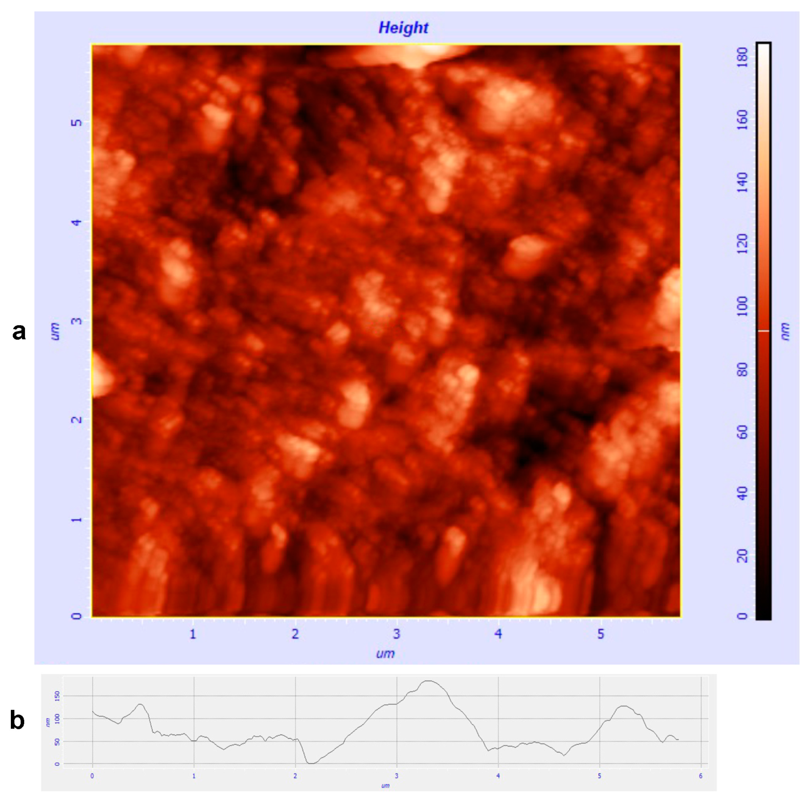
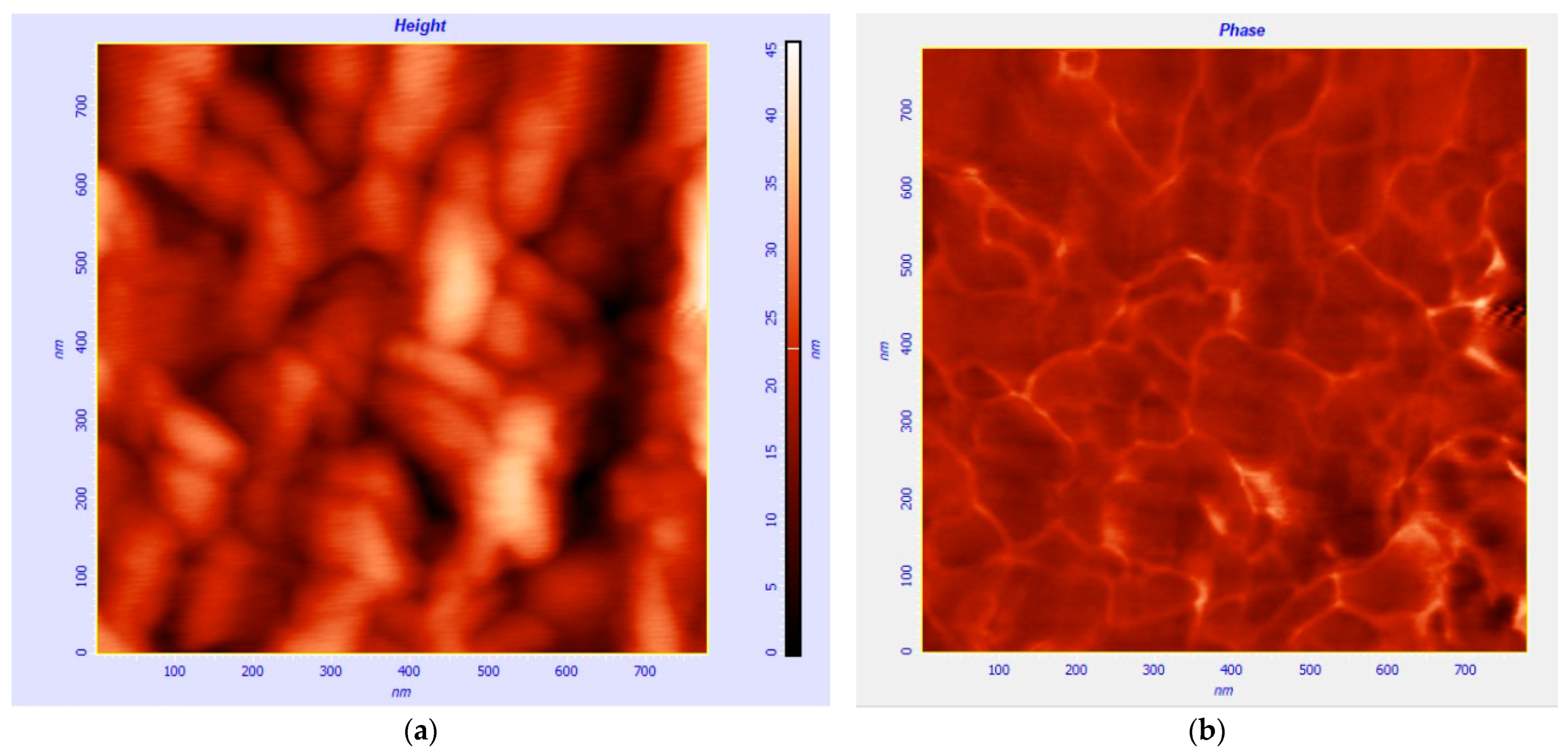
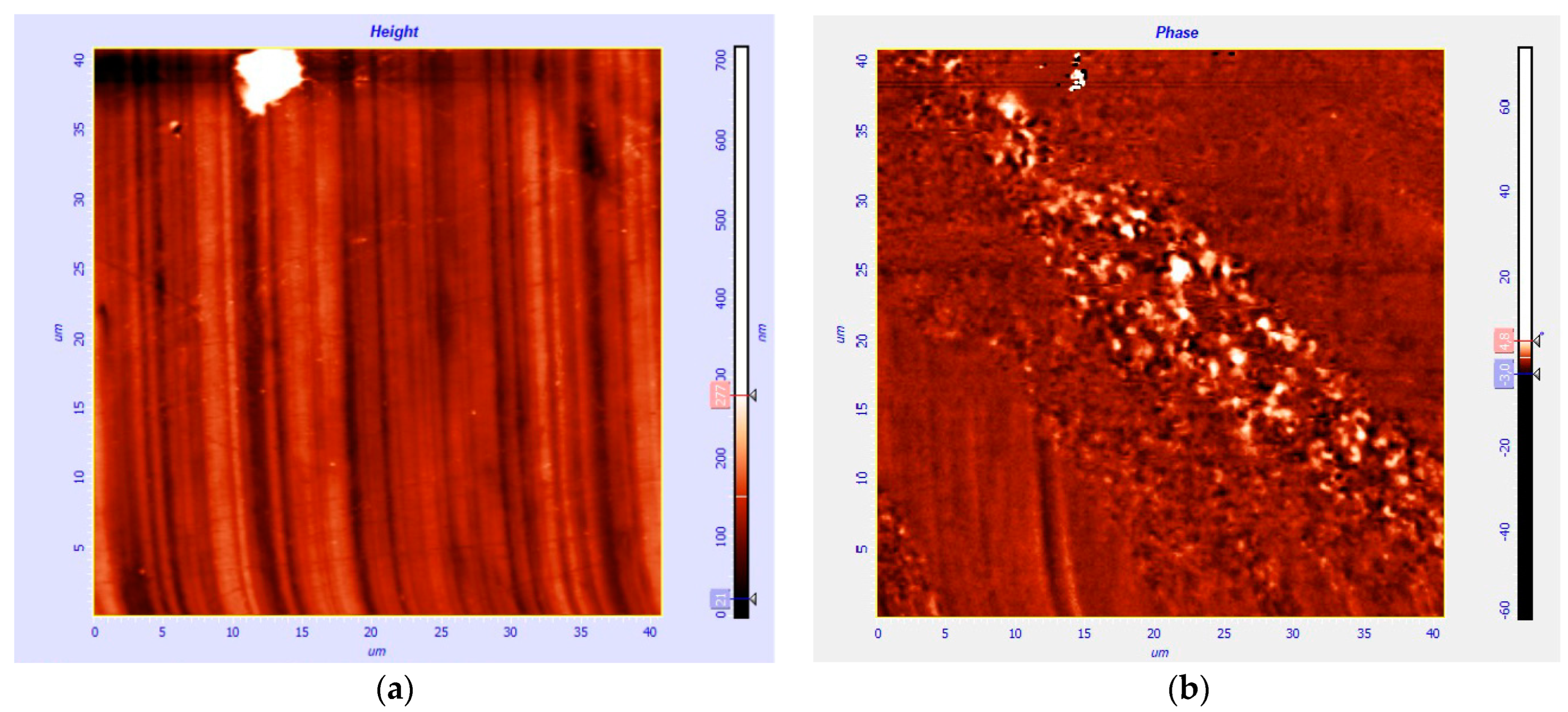
An intermetallic Nd-Pr-Fe-Co-Ti-Zr-B material with stoichiometry close to Nd2Fe14B was chosen as a convenient model material to show the wide possibilities of AFM analysis. Specifically, MQP-S-11-9-20001 [35] magnetic powder with spherical particles was used to synthesize volumetric 3D samples by means of the LPBF technique. A detailed analysis of the powder was performed in a previous study [36], including the morphology, flowability, particle size distribution, and elemental and phase composition analyses. An Addsol D50 (Moscow, Russia) 3D printing machine equipped with a 400 W power ytterbium fiber laser (IPG Photonics, Oxford, MA, USA) of 1064 nm wavelength and a 80 μm laser spot size was used for LPBF synthesis. Cubic samples with a size of 5 mm × 5 mm × 5 mm were printed using a double exposure scanning strategy, as described in [36] (sample 2.16).
Images of the surface morphology were obtained via AFM analysis using a SMENA-A scanning probe microscope (Solver platform, ZAO NT-MDT, Russia). Standard HA_NC ETALON silicon cantilevers with resonant frequencies from 110 to 235 kHz and NSG 03 frequencies of 300–400 kHz were utilized. To identify the shape and size of the grain structure of the synthesized 3D samples, the surface was etched with a 5% solution of HCl in alcohol. Magnetic force microscopy (MFM) was conducted on the smoothing of the areas of the sample’s surface using MFM01 cantilevers with 70–110 kHz frequencies and a 40 nm curvature radius. The AFM studies were carried out in semi-contact mode using the phase contrast method. NOVA software was used to process the images.
SEM images of the sample surface were taken using TESCAN Vega 3 (Brno, Czech Republic) equipment in back-scattering electron mode with 5000× magnification.

3. Results

The Nd-Fe-B material is based on a brittle intermetallic phase with poor processability via LPBF, which leads to low density in the as-built state in view of cracks, pores, and voids. In addition, the high cooling rates (~105–107 K/s) inherent in the LPBF predetermine the ultrafine grain structure of the material, including nano-sized grains and sub-grains, what is a complicated task using ordinary analytical equipment such as SEM [37]. The formation of nano-sized grains in Nd-Fe-B material after LPBF was also shown by Kim et al. [38]. AFM analysis is appropriate for this purpose due to its higher resolution and other advantages including its easy sample preparation. The Nd-Fe-B material was chosen as a suitable one to show the capabilities and limitations of AFM analysis applied to a LPBF substance. Figure 1a represents the microstructure of a 3D sample after etching, and the area of 6 μm × 6 μm was scanned. The fine grain structure is clearly visible, and the average grain size was estimated as ~100 nm. It should be noted that the grain size analysis via AFM can be considered as reliable based on the previous studies, which are in good agreement with the results obtained via AFM and X-ray diffraction [39,40]. In addition, AFM allows visualization of the height profile of the surface along the chosen line (see Figure 1b), giving additional information about the surface morphology and microstructure features, which is generally impossible to demonstrate using SEM and/or TEM methods.
AFM, in comparison with SEM facilities, possesses higher resolution up to the atomic level [41]. The maximum SEM resolution is close to AFM; however, SEM is more expensive equipment, and it is not always easily accessible to users. In comparison to AFM, an SEM image of the same surface is presented in Figure 2. A 5000× magnification was set, which gives a 40 μm × 40 μm area. However, even for the higher magnification of SEM images, a significant increase in detailing would not be achieved for the specific high-resolution mode of SEM, which was used here. No grain structure can be discerned, since the average size of the structural element was smaller than the resolution. This example shows that the main advantage of the AFM method compared to the SEM is the better resolution of the microstructure of the LPBF materials, since most of them have a fine grain structure because of the high cooling range inherent in this synthesis approach.
Moreover, the AFM image shown in Figure 1 did not represent the maximum resolution of the AFM. A square area with an 800 nm edge was scanned via AFM, and it is depicted in Figure 3a. Small grains are clearly visible; however, the used magnification is close to the limit since the edges of the elements are not sharp. A further magnification increase will not give any significant improvement in structural detail. Thus, it can be concluded that the AFM method opens the possibility to investigate fine structures with grain size up to ~10 nm and larger. The resolution depends on the specific equipment and other factors (generally, the resolution of AFM reaches 1 nm); however, the mentioned approximate value could be taken into account for structural investigations in the case of working with average equipment. It should be noted that this resolution is suitable for most cases of LPBF material analysis, since high cooling rates during the LPBF process are still lower than that for rapid quenching/melt spinning, which often leads to nano-sized grain formation (less than 10 nm) and even amorphization. The disadvantage of AFM compared to SEM is the small scanning field size, which makes the method unsuitable for observation of structural defects like pores and cracks.
AFM resolution is comparable with TEM analysis, which works on a near-atomic level. However, AFM has a few essential advantages. The AFM method is much easier to perform due to easier sample preparation (only the flat surface of the sample and etching are needed). In addition, it is much more affordable and requires less-experienced staff to operate. Thus, AFM can be a good replacement for TEM analysis when mostly surface morphology and grain structure analysis are needed without demand to thoroughly investigate the microstructure and phase composition.
Taking into account the microstructure anisotropy of 3D-printed materials synthesized via LPBF, the simplicity of the sample preparation for AFM analysis becomes significant. In most cases, both the XY and XZ cross sections of a printed sample should be studied. For AFM, only polishing/cutting and etching are needed, and it could be conducted on one cubic sample. For TEM, where thin foil is explored, and analysis can be executed only in one plane, more samples are needed to provide full data.
Another feature of AFM should be noted: magnetic cantilevers allow scanning a picture of the magnetic forces’ distribution over a surface (see Figure 3b for example), which is essential in the case of magnetic materials study. It is not a common task in the context of LPBF, however, the 3D-printing of magnetic materials and permanent magnets is now a scientific focus [36,42,43]. Thus, this feature can be crucial for some specific research. The comparison of AFM and MFM analysis, in particular, makes it is easy to control the magnetic state of grains (single- or multidomain). An interesting case of structural analysis is presented in Figure 4. Figure 4a shows an area of a not-etched surface, where no grain structure is visible, while Figure 4b is the MFM picture of the same area. Different regions with finer domains and boundary regions with larger domains are clearly visible, thus giving an approximate picture of the grain structure and melt pool boundaries of the magnetic material after LPBF without etching of its surface.
Summarizing the above discussion, the most significant advantages and disadvantages of AFM analysis are given in Table 1 in comparison with SEM and TEM. Another advantage of AFM, which should be noticed, is a tabletop size of the equipment, which does not require inert gas and/or a vacuum to operate. As a result of this, AFM equipment is more affordable than any SEM or especially TEM. The only issue concerns the frequent cantilever replacement, which is the main consumable and has a relatively high cost. It should be noted that the discussion and conclusions are given in terms of its application for 3D-printed metallic materials via the LPBF method. Other materials science fields for these analytical methods could imply other specific tasks, and other features of each microscopic method may be indispensable. Additionally, SEM extensions should be noted, such as EDS and EBSD, which expand the scope of SEM application significantly allowing investigation of the chemical composition and crystallographic orientation of grains in the scanned area.

4. Conclusions

The comprehensive research and given examples show the promise of using the AFM technique for LPBF material microstructure investigations. The high resolution, easy sample preparation, low price, and size of the equipment make the AFM investigation process facile and fast, all of which are among the main advantages of the method. It enables observing the grain structure of the metallic material after 3D-printing in the grain size range from ~10 nm. For some specific research tasks, MFM analysis is essential. The impossibility of carrying out chemical and phase composition analysis is an undeniable limitation of the AFM method; however, in many practical cases there is no need for this research. Thus, it was shown that the AFM analytical method can be used more often than it is now in the metal additive manufacturing industry, especially in small laboratories and enterprises due to the affordable equipment of atomic force microscopy compared to SEM and TEM.

Author Contributions

Conceptualization, writing—original draft preparation, I.A.P.; methodology, T.P.K.; writing—review and editing, E.L.D.; investigation, S.V.C. and K.B.L. All authors have read and agreed to the published version of the manuscript.

Funding

The study was supported by the Russian Science Foundation, project No. 19-79-30025.

Data Availability Statement

The data presented in this study are available on request from the corresponding author. The data are not publicly available due to privacy.

Conflicts of Interest

The authors declare no conflicts of interest.

References

  1. Durai Murugan, P.; Vijayananth, S.; Natarajan, M.P.; Jayabalakrishnan, D.; Arul, K.; Jayaseelan, V.; Elanchezhian, J. A Current State of Metal Additive Manufacturing Methods: A Review. Mater. Today Proc. 2022, 59, 1277–1283. [Google Scholar] [CrossRef]
  2. Attaran, M. The Rise of 3-D Printing: The Advantages of Additive Manufacturing over Traditional Manufacturing. Bus. Horiz. 2017, 60, 677–688. [Google Scholar] [CrossRef]
  3. Zhang, H.; Vallabh, C.K.P.; Zhao, X. Registration and Fusion of Large-Scale Melt Pool Temperature and Morphology Monitoring Data Demonstrated for Surface Topography Prediction in LPBF. Addit. Manuf. 2022, 58, 103075. [Google Scholar] [CrossRef]
  4. Chowdhury, S.; Yadaiah, N.; Prakash, C.; Ramakrishna, S.; Dixit, S.; Gupta, L.R.; Buddhi, D. Laser Powder Bed Fusion: A State-of-the-Art Review of the Technology, Materials, Properties & Defects, and Numerical Modelling. J. Mater. Res. Technol. 2022, 20, 2109–2172. [Google Scholar] [CrossRef]
  5. Aboulkhair, N.T.; Simonelli, M.; Parry, L.; Ashcroft, I.; Tuck, C.; Hague, R. 3D Printing of Aluminium Alloys: Additive Manufacturing of Aluminium Alloys Using Selective Laser Melting. Prog. Mater. Sci. 2019, 106, 100578. [Google Scholar] [CrossRef]
  6. Ahn, B. Microstructural Tailoring and Enhancement in Compressive Properties of Additive Manufactured Ti-6Al-4V Alloy through Heat Treatment. Materials 2021, 14, 5524. [Google Scholar] [CrossRef]
  7. Jeyaprakash, N.; Saravana Kumar, M.; Yang, C.-H.; Cheng, Y.; Radhika, N.; Sivasankaran, S. Effect of Microstructural Evolution during Melt Pool Formation on Nano-Mechanical Properties in LPBF Based SS316L Parts. J. Alloys Compd. 2024, 972, 172745. [Google Scholar] [CrossRef]
  8. Rani, S.U.; Kesavan, D.; Kamaraj, M. Evaluation of Influence of Microstructural Features of LPBF Ti-6Al-4 V on Mechanical Properties for an Optimal Strength and Ductility. J. Alloys Compd. 2023, 960, 170575. [Google Scholar] [CrossRef]
  9. Herzog, D.; Seyda, V.; Wycisk, E.; Emmelmann, C. Additive Manufacturing of Metals. Acta Mater. 2016, 117, 371–392. [Google Scholar] [CrossRef]
  10. Zheng, T.; Pan, S.; Murali, N.; Li, B.; Li, X. Selective Laser Melting of Novel 7075 Aluminum Powders with Internally Dispersed TiC Nanoparticles. Mater. Lett. 2022, 319, 132268. [Google Scholar] [CrossRef]
  11. Liu, G.; Zhou, S.; Wang, C.; Chen, S.; Sun, D.; Chen, A.; Li, Z.; Yan, C.; Shi, Y. Fabrication and Characterization of SiC/Al Composites Prepared by Laser Powder Bed Fusion (LPBF) Combined with Vacuum Pressure Infiltration. Mater. Des. 2023, 236, 112495. [Google Scholar] [CrossRef]
  12. Spierings, A.B.; Ozherelkov, D.Y.; Kneubühler, F.; Eremin, S.A.; Pelevin, I.A.; Nalivaiko, A.Y.; Petrov, E.A.; Gromov, A.A.; Wegener, K. Laser Powder Bed Fusion of AlSi10Mg-Based Composites with Graphene and Nanodiamond Additions. J. Alloys Compd. 2023, 947, 169421. [Google Scholar] [CrossRef]
  13. Li, S.; Yue, X.; Li, Q.; Peng, H.; Dong, B.; Liu, T.; Yang, H.; Fan, J.; Shu, S.; Qiu, F.; et al. Development and Applications of Aluminum Alloys for Aerospace Industry. J. Mater. Res. Technol. 2023, 27, 944–983. [Google Scholar] [CrossRef]
  14. Bai, J.; Yang, Y.; Wen, C.; Chen, J.; Zhou, G.; Jiang, B.; Peng, X.; Pan, F. Applications of Magnesium Alloys for Aerospace: A Review. J. Magnes. Alloys 2023, 11, 3609–3619. [Google Scholar] [CrossRef]
  15. Sanchez, S.; Smith, P.; Xu, Z.; Gaspard, G.; Hyde, C.J.; Wits, W.W.; Ashcroft, I.A.; Chen, H.; Clare, A.T. Powder Bed Fusion of Nickel-Based Superalloys: A Review. Int. J. Mach. Tools Manuf. 2021, 165, 103729. [Google Scholar] [CrossRef]
  16. Alkhatib, S.E.; Sercombe, T.B. High Strain-Rate Response of Additively Manufactured Light Metal Alloys. Mater. Des. 2022, 217, 110664. [Google Scholar] [CrossRef]
  17. Qin, Y.; Wen, P.; Guo, H.; Xia, D.; Zheng, Y.; Jauer, L.; Poprawe, R.; Voshage, M.; Schleifenbaum, J.H. Additive Manufacturing of Biodegradable Metals: Current Research Status and Future Perspectives. Acta Biomater. 2019, 98, 3–22. [Google Scholar] [CrossRef]
  18. Bernhardt, A.; Schneider, J.; Schroeder, A.; Papadopoulous, K.; Lopez, E.; Brückner, F.; Botzenhart, U. Surface Conditioning of Additively Manufactured Titanium Implants and Its Influence on Materials Properties and in Vitro Biocompatibility. Mater. Sci. Eng. C 2021, 119, 111631. [Google Scholar] [CrossRef]
  19. Chernyshikhin, S.V.; Mahato, B.; Shiverskii, A.V.; Pelevin, I.A.; Dubinin, O.N.; Egorov, V.Y.; Abaimov, S.G.; Shishkovsky, I.V. In-Plane Measurements and Computational Fluid Dynamics Prediction of Permeability for Biocompatible NiTi Gyroid Scaffolds Fabricated via Laser Powder Bed Fusion. Int. J. Bioprinting 2023, 10, 0119. [Google Scholar] [CrossRef]
  20. Nagarajan, B.; Hu, Z.; Song, X.; Zhai, W.; Wei, J. Development of Micro Selective Laser Melting: The State of the Art and Future Perspectives. Engineering 2019, 5, 702–720. [Google Scholar] [CrossRef]
  21. Finazzi, V.; Berti, F.; Guillory II, R.J.; Petrini, L.; Previtali, B.; Demir, A.G. Patient-Specific Cardiovascular Superelastic NiTi Stents Produced by Laser Powder Bed Fusion. Procedia CIRP 2022, 110, 242–246. [Google Scholar] [CrossRef]
  22. Wu, Y.; Liu, J.; Kang, L.; Tian, J.; Zhang, X.; Hu, J.; Huang, Y.; Liu, F.; Wang, H.; Wu, Z. An Overview of 3D Printed Metal Implants in Orthopedic Applications: Present and Future Perspectives. Heliyon 2023, 9, e17718. [Google Scholar] [CrossRef] [PubMed]
  23. Whitesides, G.M. The Origins and the Future of Microfluidics. Nature 2006, 442, 368–373. [Google Scholar] [CrossRef]
  24. Hirt, L.; Reiser, A.; Spolenak, R.; Zambelli, T. Additive Manufacturing of Metal Structures at the Micrometer Scale. Adv. Mater. 2017, 29, 1604211. [Google Scholar] [CrossRef]
  25. Gale, W.F.; Newcomb, S.B.; Totemeier, T.C.; Vander Voort, G.F. Metallography. In Smithells Metals Reference Book; Elsevier: Amsterdam, The Netherlands, 2004; pp. 10-1–10-87. [Google Scholar]
  26. Pelevin, I.A.; Ozherelkov, D.Y.; Nalivaiko, A.Y.; Bodyakova, A.I.; Chernyshikhin, S.V.; Zotov, B.O.; Korshunov, A.V.; Gromov, A.A. AlSi10Mg/AlN Interface Grain Structure after Laser Powder Bed Fusion. Metals 2022, 12, 2152. [Google Scholar] [CrossRef]
  27. Keya, T.; Bikmukhametov, I.; Shmatok, A.; Harvill, G.; Brewer, L.N.; Thompson, G.B.; Andurkar, M.; Thompson, S.M.; O’Donnell, V.; Gahl, J.; et al. Evolution of Microstructure and Its Influence on the Mechanical Behavior of LPBF Inconel 625 upon Direct Aging. Manuf. Lett. 2023, 35, 732–742. [Google Scholar] [CrossRef]
  28. Qin, H.; Fallah, V.; Dong, Q.; Brochu, M.; Daymond, M.R.; Gallerneault, M. Solidification Pattern, Microstructure and Texture Development in Laser Powder Bed Fusion (LPBF) of Al10SiMg Alloy. Mater. Charact. 2018, 145, 29–38. [Google Scholar] [CrossRef]
  29. Abd Mutalib, M.; Rahman, M.A.; Othman, M.H.D.; Ismail, A.F.; Jaafar, J. Scanning Electron Microscopy (SEM) and Energy-Dispersive X-Ray (EDX) Spectroscopy. In Membrane Characterization; Elsevier: Amsterdam, The Netherlands, 2017; pp. 161–179. [Google Scholar]
  30. Ernould, C.; Beausir, B.; Fundenberger, J.-J.; Taupin, V.; Bouzy, E. Applications of the Method. In Advances in Imaging and Electron Physics; Elsevier: Amsterdam, The Netherlands, 2022; Volume 223, pp. 155–215. [Google Scholar]
  31. Barmak, K. Crystal Orientation Mapping in Scanning and Transmission Electron Microscopes. In Metallic Films for Electronic, Optical and Magnetic Applications; Elsevier: Amsterdam, The Netherlands, 2014; pp. 39–66. [Google Scholar]
  32. García-Moreno, F.; Neu, T.R.; Kamm, P.H.; Banhart, J. X-ray Tomography and Tomoscopy on Metals: A Review. Adv. Eng. Mater. 2023, 25, 2201355. [Google Scholar] [CrossRef]
  33. Gulati, K.; Adachi, T. Profiling to Probing: Atomic Force Microscopy to Characterize Nano-Engineered Implants. Acta Biomater. 2023, 170, 15–38. [Google Scholar] [CrossRef]
  34. Li, M. Fundamentals and Methods of Atomic Force Microscopy for Biophysics. In Atomic Force Microscopy for Nanoscale Biophysics; Elsevier: Amsterdam, The Netherlands, 2023; pp. 1–42. [Google Scholar]
  35. MQP-S-11-9-20001. Available online: https://mqitechnology.com/product/mqp-s-11-9-20001/ (accessed on 30 August 2024).
  36. Pelevin, I.A.; Terekhin, E.A.; Ozherelkov, D.Y.; Tereshina, I.S.; Karpenkov, D.Y.; Bochkanov, F.Y.; Chernyshikhin, S.V.; Nalivaiko, A.Y.; Gromov, A.A. New Scanning Strategy Approach for Laser Powder Bed Fusion of Nd-Fe-B Hard Magnetic Material. Metals 2023, 13, 1084. [Google Scholar] [CrossRef]
  37. Hooper, P.A. Melt Pool Temperature and Cooling Rates in Laser Powder Bed Fusion. Addit. Manuf. 2018, 22, 548–559. [Google Scholar] [CrossRef]
  38. Kim, H.-J.; Jang, Y.R.; Lee, H.-S.; Cho, J.-W.; Jang, T.; Eo, D.-R.; Lee, W. Microstructural Investigation of Nanocrystalline Nd-Fe-B Magnets Fabricated by Laser Powder Bed Fusion. Mater. Charact. 2024, 216, 114228. [Google Scholar] [CrossRef]
  39. Tereshina, I.S.; Pelevin, I.A.; Tereshina, E.A.; Burkhanov, G.S.; Rogacki, K.; Miller, M.; Kudrevatykh, N.V.; Markin, P.E.; Volegov, A.S.; Grechishkin, R.M.; et al. Magnetic Hysteresis Properties of Nanocrystalline (Nd,Ho)-(Fe,Co)-B Alloy after Melt Spinning, Severe Plastic Deformation and Subsequent Heat Treatment. J. Alloys Compd. 2016, 681, 555–560. [Google Scholar] [CrossRef]
  40. Andreeva, N.V.; Filimonov, A.V.; Rudskoi, A.I.; Burkhanov, G.S.; Tereshina, I.S.; Politova, G.A.; Pelevin, I.A. A Study of Nanostructure Magnetosolid Nd–Ho–Fe–Co–B Materials via Atomic Force Microscopy and Magnetic Force Microscopy. Phys. Solid State 2016, 58, 1862–1869. [Google Scholar] [CrossRef]
  41. Ohnesorge, F.; Binnig, G. True Atomic Resolution by Atomic Force Microscopy Through Repulsive and Attractive Forces. Science 1993, 260, 1451–1456. [Google Scholar] [CrossRef]
  42. Tosoni, O.; Mendonça, E.B.; Reijonen, J.; Antikainen, A.; Schäfer, L.; Riegg, S.; Gutfleisch, O. High-Coercivity Copper-Rich Nd-Fe-B Magnets by Powder Bed Fusion Using Laser Beam Method. Addit. Manuf. 2023, 64, 103426. [Google Scholar] [CrossRef]
  43. Goll, D.; Trauter, F.; Bernthaler, T.; Schanz, J.; Riegel, H.; Schneider, G. Additive Manufacturing of Bulk Nanocrystalline FeNdB Based Permanent Magnets. Micromachines 2021, 12, 538. [Google Scholar] [CrossRef]
Figure 1. AFM image of the Nd-Fe-B etched surface (a) and its height profile along the top edge of the scanned area (b).
Compounds 04 00034 g001
Figure 2. SEM image of the same LPBF sample’s surface shown in Figure 1.
Compounds 04 00034 g002
Figure 3. High resolution AFM image (a) and MFM image of the same area (b).
Compounds 04 00034 g003
Figure 4. AFM (a) and MFM (b) images of the same region of the Nd-Fe-B sample on a not-etched surface.
Compounds 04 00034 g004
Table 1. Advantages and disadvantages of the AFM, SEM, and TEM methods applied to the microstructure analysis of LPBF metallic materials.
CharacteristicAFMSEMTEM
Advantages
-
High resolution
-
Easy sample preparation
-
Ability to investigate magnetic domain structure
-
Small size and affordable equipment
-
Easy sample preparation
-
Ability to investigate chemical composition (+EDX)
-
High resolution
-
Ability to investigate phase composition (+XPS)
Disadvantages
-
Expensive consumables (cantilevers)
-
Impossibility of investigating chemical and phase composition
-
Relatively low resolution
-
Expensive and large equipment
-
Expensive and large equipment
-
Difficult sample preparation
Disclaimer/Publisher’s Note: The statements, opinions and data contained in all publications are solely those of the individual author(s) and contributor(s) and not of MDPI and/or the editor(s). MDPI and/or the editor(s) disclaim responsibility for any injury to people or property resulting from any ideas, methods, instructions or products referred to in the content.

