Article

Synthesis and Functionalities of Blade-Coated Nanographite Films

by
Paloma E. S. Pellegrini
1,*,†,
Luana de Moraes Leitão Gonçalves Vaz
2,
Silvia Vaz Guerra Nista
1,*,†,
Hugo Enrique Hernández-Figueroa
2 and
Stanislav Moshkalev
1,†
1
Center for Semiconductor Components and Nanotechnology, Universidade Estadual de Campinas, Campinas 13083-870, Brazil
2
School of Electrical and Computer Engineering, Universidade Estadual de Campinas, Campinas 13083-852, Brazil
*
Authors to whom correspondence should be addressed.
Current address: João Pandia Calógeras, 90, Campinas 13083-870, SP, Brazil.
Micro 2024, 4(3), 460-473; https://doi.org/10.3390/micro4030029
Submission received: 6 June 2024 / Revised: 11 July 2024 / Accepted: 17 July 2024 / Published: 27 July 2024
(This article belongs to the Special Issue Advances in Micro- and Nanomaterials: Synthesis and Applications)

Abstract

:
The manufacturing and characterization of nanographite films on substrates form the foundation for advances in materials science. Conductive graphite films are challenging products, as isolating graphite oxide is often necessary. In this study, nanographite suspensions containing non-oxidized graphite flakes were used to fabricate novel thin and ultrathin films via blade coating on industry-standard substrates. Films as thin as 346 nm were successfully fabricated. Moreover, it was possible to induce the orientation of the graphite nanoflakes via blade coating. This orientation led to electrical anisotropy; thus, the electrical behavior of the films in each orthogonal direction differed. After adjusting the coating parameters and the concentration of the nanographite flakes, the electrical conductivity ranged from 0.04 S/cm to 0.33 S/cm. In addition, with such adjustments, the transparency of the films in the visible range varied from 20% to 75%. By establishing a methodology for the tuning of both electrical and optical properties via adjustments in the nanographite suspension and coating parameters, we can fabricate resistant, conductive, and transparent films satisfying certain requirements. The results presented here can be extrapolated to enhance applications, especially for photonics and solar cells, in fields that require electrical conductive materials with high levels of transparency.

1. Introduction

Graphitic materials have revolutionized materials science and play a crucial role in myriad fields, such as nano- and micro-technology, energy, and even biosensing. Through comprehending and shaping their properties, carbon materials have had a significant impact on science, and efforts to manufacture graphite-based thin films have changed the roadmap in microelectronics for the better [1].
Bulk graphite is composed of a layered hexagonal carbon structure that is coupled because of van der Waals interactions, where the carbon atoms in each layer are strongly linked via covalent bonds. One of the greatest breakthroughs in carbon science was to find that a few layers or a single layer of graphite (i.e., graphene) presents distinct and peculiar properties compared to the bulk material [2]. Among its many characteristics, the room temperature Hall effect, the anisotropic electric field, and the degeneration between the conduction and valence band at the K point [3,4] stand out. These extraordinary properties make graphite films advantageous materials in science. The challenge is to produce thin and stable films that can be used to explore these properties, ideally at large scales.
Several techniques to fabricate ultrathin graphite and graphene films have been proposed and used over the years, such as mechanical exfoliation [5], chemical vapor deposition (CVD) [6], layer-by-layer assembly [7], lithography [8], colloidal suspensions [9], and spin coating [10].
Mechanical exfoliation was the first top-down alternative for fabricating graphene sheets [4], with large areas and high quality, although its major drawbacks include reproducibility and scalability difficulties. The same reasoning is applied to mechanical cleavage, while milling can cause defects in the graphene structure [11].
It has been reported that CVD is a well-established bottom-up fabrication method for thin films. Its high quality, reproducibility, and large-area (up to centimeters) deposition are required characteristics for practical applications [6]; however, the complexity of the method makes scalability a challenge.
Nanographite flakes are graphite grains that have been exfoliated, so each flake consists of only a few layers of graphene. Although their surface area can reach a few square micrometers, the thickness of each flake is nanometric. The development of suspensions of nanographite broadens the available fabrication techniques to include well-established film formation through spin coating. Usually, to prepare graphite oxide (GO), the colloidal suspensions are based on mineral acids with agents to achieve oxidation [12]. Among the preparation methods, the Hummers–Offeman method stands out [13,14,15]. Typically using graphite flakes, acidic agents diffuse in the interlayers of graphite to form pristine oxidized graphite. After rinsing with water, the GO is obtained in solution in nano- and micro-metric grains. Although the manufacturing process has been well-reported, GO films exhibit electrical insulating properties with little room for improvement.
The formation of ultrathin graphite films via spin coating from suspensions began to produce significant research once it became possible to explore the peculiar characteristics of graphite in a practical film, for example, its non-linearities and thermal and electric conductivity [16,17,18]. Nonetheless, the stability and homogeneity of the solution are still issues to be overcome.
In this work, we propose an alternative for fabricating thin and ultrathin graphitic films and, thereby, tune the electric direct current (DC) response and transparency in the visible range.
Contrary to usual suspensions based only on deionized water, we propose the addition of sodium silicate (Na2SiO3) in graphitic suspensions to form resistant films. It is water soluble, and its transparency makes it a viable solution for photonic and solar cell applications. However, its addition introduces some areas of concern, such as homogeneity and pH control [19]. We innovatively utilize a non-oxidized nanographite suspension that contains sodium silicate and a surfactant to fabricate thin films [20].
We novelly integrate this suspension with the blade-coating technique to fabricate thin films on standard substrates such as silica. In addition, to the best of our knowledge, this is the first time that the conductivity and transparency of graphite films have been tuned as a result of adjustments in the concentration of nanographite in the suspension and the optimization of parameters from blade coating.
Blade coating, on the other hand, brings advantages of scalability, large-area deposition, and homogeneity when compared to spin coating and is much less complex than CVD. With a unidirectional roll, a blade drags the meniscus of the fluid at a controlled velocity while a hot plate evaporates the solvents. Thickness control of the films is usually achieved by controlling the speed and the height of the blade [21,22].
In this study, different parameters are optimized to perform thickness control, including the volume of the deposited fluid and the shape of the blade utilized. An efficient thickness control leads to a better understanding of the electrical and optical properties of the fabricated films.
In addition, because of the deposition method, the orientation of the nanographite flakes is controlled during coating. This organization of the nanographite flakes significantly affects the electric field distribution; thus, the films are highly anisotropic, favoring the flow of the electric current in a certain direction.
The films, manufactured using the aforementioned method, are characterized according to their optical and electrical properties: transparency in the visible range, X-ray diffraction patterns, Raman spectroscopy, and electrical conductivity in the DC regime.

2. Materials and Coating Method

A stable and homogenous graphitic suspension was used. It contained sodium silicate, commonly known as water glass, acquired from Sigma Aldrich 338443 (Merck KGaA, Darmstadt, Germany), deionized water, and a non-ionic surfactant (Sigma Aldrich, Merck KGaA, Darmstadt, Germany), in addition to nanographite flakes. The graphite used was Micrograf 99507UJ, commercially available from Nacional de Grafite (Minas Gerais, Brazil). This material was laminated, with a few stacked layers of graphite and average widths of approximately 1 μm in diameter, and the thickness of the graphite flakes was up to 30 nm [20].
Different concentrations of nanographite were prepared in the suspension in order to obtain reproducible thin films with distinct optical and electrical characteristics, as described in the following sections. The nanographite concentration varied from 4% to 25%.
Once the suspensions with different concentrations were prepared, the blade-coating technique was used to coat them on glass substrates. This work details the optimal range of deposition parameters that enables the formation of thin and ultrathin nanographite films.
The equipment used for coating was the Blade Coater BCC-02 from AutoCoat. It is compact, 52 × 29 × 36 cm, with a coating area of up to 49 cm2. The speed of the blade is controlled via embedded motor systems and ranges from 0.5 to 40 mm/s. The machinery includes a hot plate, where the substrate is placed, held with vacuum pumps. The temperature of the hot plate can reach 150 °C.
In short, blade coating is based on dragging the meniscus of a fluid onto a substrate while evaporating its solvents.
An illustration of the blade-coating technique for the nanographite suspension used on the glass substrate can be seen in Figure 1. In this process, it is possible to choose different types of blades that impact the film thickness, as demonstrated. The illustration depicts two of them, beveled and cylindrical.
While the blade travels and drags the fluid, two different types of meniscus, advancing and receding, are formed on both sides of the chosen blade. The advancing meniscus affects how and at what speed the fluid is spread on the substrate, and the receding meniscus dictates the uniformity and the thickness of the coated film [23]. As for the dragging direction, it influences the alignment of the nanographite flakes.
The meniscus deposition process is governed by two regimes: the Landau–Levich regime and evaporation. The first one is characterized by an excessive supply rate of solvent compared to the evaporation rate. In this regime, the shaping, leveling, and drying processes are separate events in time. Such situations are generally avoided in the context of thin films. In contrast, the evaporation regime maintains a proportional relationship between the meniscus dragging and solvent evaporation rates [24].
During the deposition process, a thickness gradient—referred to as wet and dry—is formed from the solvent’s evaporation process, as shown in Figure 1. The wet thickness stage occurs before the evaporation process. Once the solvent has evaporated, the film reaches its final dry thickness [25]. This gradient mainly arises from the relationship between the fluid deposition rate and the solvent evaporation rate. In this respect, there is an optimized combination of the blade speed and the hot plate temperature, enabling the system to be in an evaporation regime.
Therefore, properly determining the hot plate temperature is crucial for an optimized coating. Based on empirical methods, the temperature was set at 70 °C to fit the evaporation regime. The final deposition result was consequently a film composed of nanographite flakes and sodium silicate adhered to the substrate.
Moreover, a post-baking process at 200 °C was performed in order to ensure the evaporation of the remaining solvents and, thus, improve adherence. With excellent adherence, the nanographite films were preserved even when immersed in common liftoff solvents used in various types of lithography. These include optical and nanoimprint lithography, using the solvent MIF300 [26] and acetone for thermal scanning probe lithography [27] and electron beam lithography [28].
After coating and the complete evaporation of solvents, the thickness and uniformity of the films could be measured.
The characterization of the films relied on optical microscopy (Olympus upright, UC 50 CCD; Olympus Corporation, Tokoy, Japan), scanning electron microscopy (SEM) (Hitachi S-3400N; Hitachi High-Tech, Japan), X-ray diffraction patterns (Bruker D8 Advance; Bruker Corporation, USA), Raman spectroscopy (T64000 Horiba; HORIBA Scientific, Japan), and four probe measurements (Agilent B2912A; Keysight Technologies, USA).

3. Results and Discussion of the Characterization of Nanographite Films

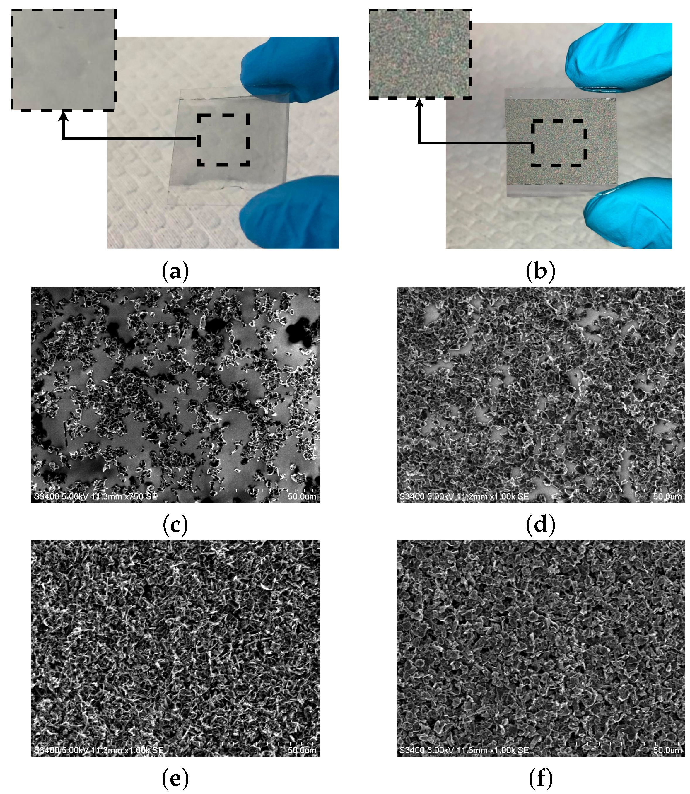
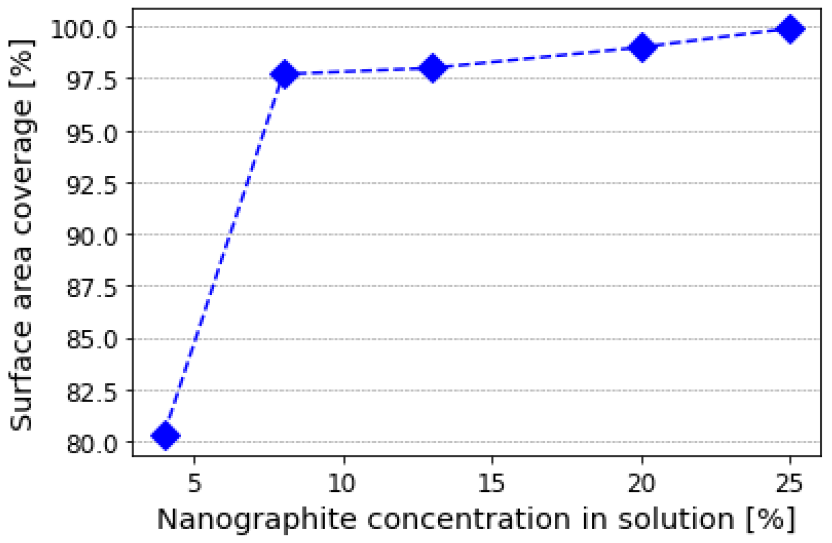
3.1. Blade-Coated Nanographite Films

In this study, concentrations from 4 % to 25 % of nanographite were used in suspensions and blade-coated on glass substrates, as described above.
Blade-coated films with 8 % and 25 % of nanographite are shown, respectively, in Figure 2a,b, post-baking. Additionally, scanning electron microscopy (SEM) images from 4 % to 25 % nanographite films can be seen in Figure 2c–f. The lighter regions of the images correspond to the sodium silicate enclosed by the nanographite flakes (dark flakes). As the concentration increased, the sodium silicate was fully covered by the flakes.
In addition, the films were analyzed according to the coverage of the superficial area of the substrate. With a 4 % nanographite concentration, up to 80 % of the area of the substrate was coated by the nanographite flakes. As the concentration increased, so did the covered area. With a graphite concentration as high as 25 % , the substrate was nearly fully coated, with a coverage area of more than 98 % . The graph in Figure 3 exhibits the experimental results obtained from the microscopy analysis.
The thickness of the films could be better controlled by both the volume of the solution deposited and the geometry of the blade. In Figure 4, we show evidence of how the volume and blade geometry affect the film thickness.
The graph shown in Figure 4 summarizes the linear relationship between the deposited volume and the thickness of the nanographite films fabricated for five nanographite concentrations in the suspension: 4 % , 8 % , 13 % , 20 % , and 25 % .
In addition, each graphite concentration allowed a certain thickness range. For instance, for the lowest graphite concentration, 4 % , with 8 µL of solution, a 346 nm-thick film was fabricated. If we compare this result with the highest graphite concentration, 25 % , a thickness of approximately 15.7 µm was measured for the same volume.
However, the relationship between the thickness and graphite concentration is not linear, and the experimental data can be exponentially fitted, as conducted in Figure 5. We notice a convergence of the data, where the increasing nanographite concentration weakly affects the thickness of the film. It is a limit above which increasing the volume of solution deposited via blade coating will not lead to thicker films, as shown in in Figure 5.
Therefore, fabricating even thinner films with a higher nanographite concentration was not enough to decrease the volume of the deposition. It was necessary to change the deposition parameters, and a fundamental one is the shape of the blade [23].
Taking, for instance, a solution with a concentration of 25 % nanographite and using the blade-coating method with a cylindrical blade instead of the beveled one, it is possible to reduce the thickness of the film by approximately 96%. For 8 µL of solution deposited, the thickness when using the beveled blade was 16.68 µm, as presented earlier. Using the cylindrical blade, the thickness was reduced to 561 nm.
The data comparing the film thicknesses using both beveled and cylindrical blades for the 25 % nanographite solution are shown in Figure 6.

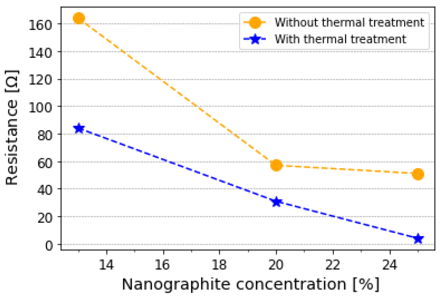
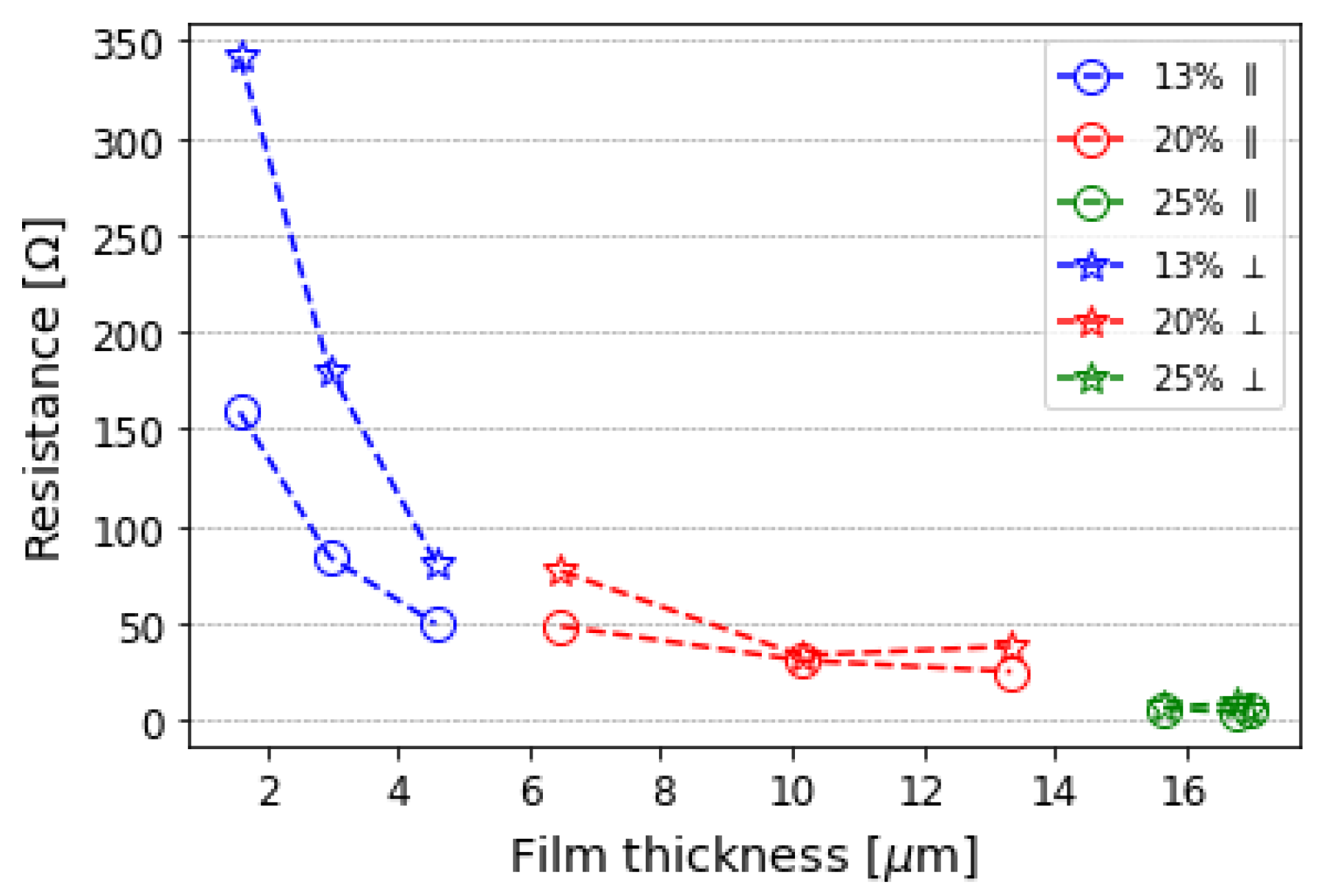
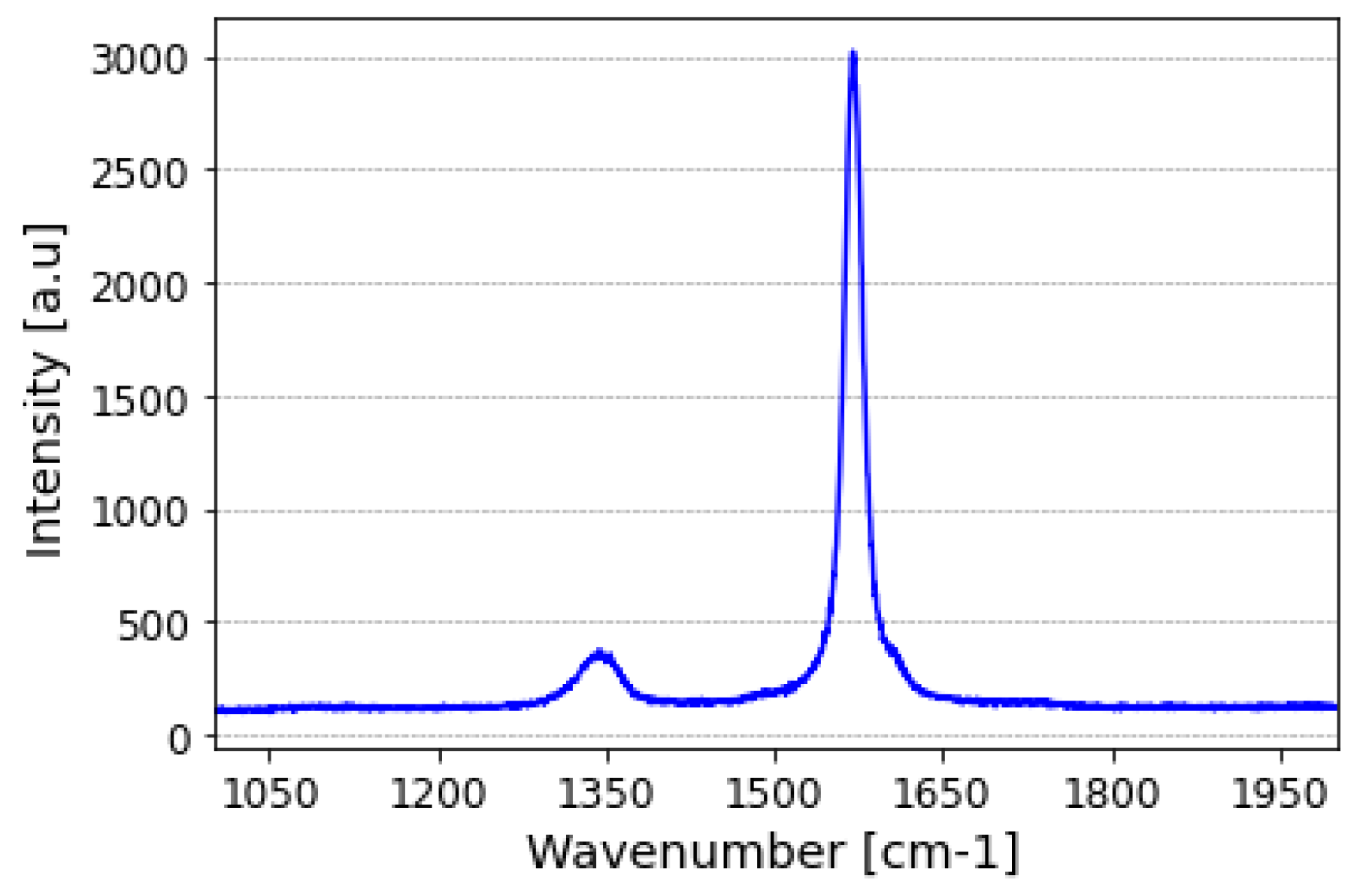
3.2. Electrical Characterization

The possibility to incorporate graphitic material and to explore its properties at micro- and nano-metric scales has impacted science. One of the many outstanding properties of these graphitic materials is their DC electrical conductivity [29].
However, the synthesis and fabrication of conductive graphitic materials remain a challenge. Usually, the graphitic solution used to fabricate the films is oxidized, which significantly affects the electrical conductivity [19].
In addition, the fabrication of thin graphite films is known to be delicate, which makes their application arduous [30].
The electrical characterization presented comes from nanographite films blade-coated using a non-oxidized nanographite suspension. In addition, the films were stable; they were manipulated for months with no signs of degradation.
The DC electrical conductivity of the nanographite films was studied using the four-probe method [31,32]. The samples were analyzed once the whole fabrication process was complete, which means post-baking.
Thermally expanding graphitic materials can enhance their electrical conductivity by up to six times because of the structural changes that occur in the process, such as the reduction in defects and the organization of the structure. However, it comes with structural drawbacks in the graphite due to thermal expansion [33].
Therefore, we aimed to find a balance between improving the electrical conductivity and preserving the graphite structure. Here, the films were fabricated—according to the method presented earlier—via blade coating using a beveled blade, and the thermal treatment was performed at 350 °C in a muffle oven, as a compromise to enhance the conductivity and avoid structural defects in the nanographite flakes.
Figure 7 shows the influence of this thermal treatment strategy. Three different films were analyzed at 13%, 20%, and 25% nanographite. These films were all fabricated with 8 µL of solution, and their thicknesses can be verified in Figure 4.
The resistance decreased by approximately half for the 13% and 20% nanographite films. For the 25% nanographite sample, the resistance decreased by 87%. This difference between films arises from the thickness range and graphite concentration that they present. We expected a more noticeable decrease with the higher graphite concentration sample, as more material was thermally treated.
Because of the blade-coating technique used to fabricate the films, they exhibited distinct electric conductivity, anisotropy, depending on how the resistance was measured. If the probes were placed so the direct current flowed parallel to the deposition direction (i.e., parallel to the direction in which the meniscus was dragged), the resistance was lower than measurements taken in the perpendicular direction to the deposition. The results shown in Figure 8 that were taken along the parallel direction to the deposition are labeled with ‖, while the ones taken in the perpendicular direction are labeled with ⊥.
Such anisotropy is the consequence of the nanographite flakes’ orientation, emphasized by the blade-coating technique.
Nanographite films with a concentration of 8 % or lower exhibited a more isolant behavior. For this sample, the resistance measured was up to 3.06 kΩ. As for higher nanographite concentrations up to 25%, the resistances in parallel inversely varied from 159 Ω to approximately 4 Ω. The resistance results are shown in Figure 8.
Note that each nanographite concentration, studied in Figure 8, allows a certain resistance range. Considering the measurements with the current flow parallel to the flake orientation, with 13% nanographite, the resistance varied from 158.8   Ω to 49.5   Ω ; with 20 % nanographite, it varied from 48 Ω to 25 Ω ; and finally, for the 25 % nanographite sample, the resistance was measured from 6 Ω to 4 Ω . It is clear that, for 25 % nanographite, the films entered a saturation regime, where the resistance did not significantly change when varying the thickness or further increasing the graphite concentration. In this range, the measurements approached asymptotic behavior, where noise and slight variations in the data were expected.
Comparing the resistances measured parallel and perpendicular to the flakes’ orientation, for the 13 % nanographite film, the perpendicular resistance is about 2.15 times the parallel resistance.
Closer to the saturation regime, the anisotropy becomes less evident: for the thinner film, with 20 % nanographite, the difference is about 1.6 times. With higher nanographite concentrations and thicker samples, it was more difficult to maintain the flakes’ orientation because of the multiple layers of nanographite. Therefore, the resistance measurements become less distinct and begin to overlap, as can be noted at the 25 % graphite concentration.
Hence, by tuning the nanographite concentration and the deposition parameters (mainly the volume deposited), it is possible to tune and predict the electrical conductivity of the film.
Considering the thickness of each sample and the parallel results of the resistances, Figure 9 presents the electrical conductivity in S.cm−1 of the graphite films fabricated. The films that presented the highest electrical conductivity were the ones with higher nanographite concentrations, 25 % , at approximately 0.33 S.cm−1. As their resistance measurements were in the asymptotic regime and there were multiple layers of nanographite, the thickness did not play a decisive role.
For the lower concentrations, the 13 % nanographite film presented higher conductivity (0.09 S.cm−1) than the 20 % graphite (0.07 S.cm−1). This difference might have been caused by the influence of the thickness.
As the thickness of the film increases, so does the number of nanographite flakes in the suspension; therefore, the organization of the flakes induced by blade coating is less influential. A smaller degree of organization of the flakes results in a less effective flow of electric current. We can see this effect in the 20% nanographite film having poorer electrical conductivity than the better-aligned film. However, increasing the number of flakes further in the 25% nanographite suspension, the conductivity increases again. In this case, we have a supersaturated-like suspension, and the number of nanographite flakes is large enough that there are no gaps between the flakes, resulting in a better flow of the current; here, the organization of the flakes does not play a role, as the flakes most likely overlap. In this case, there is no electrical anisotropy.
Hence, there is a fine balance between the nanographite concentration and the electrical conductivity. On the one hand, it is possible to obtain a conductive film with fewer nanographite flakes that are well-aligned; on the other hand, more nanographite flakes may cause the opposite result, as there are too many particles to be aligned via blade coating but not enough to fill any isolated gaps from the substrate.
Although the 20 % nanographite film is thicker, the 13 % nanographite thinner film allowed the blade-coating technique to better align the nanographite flakes and, therefore, resulted in a better DC conductivity.

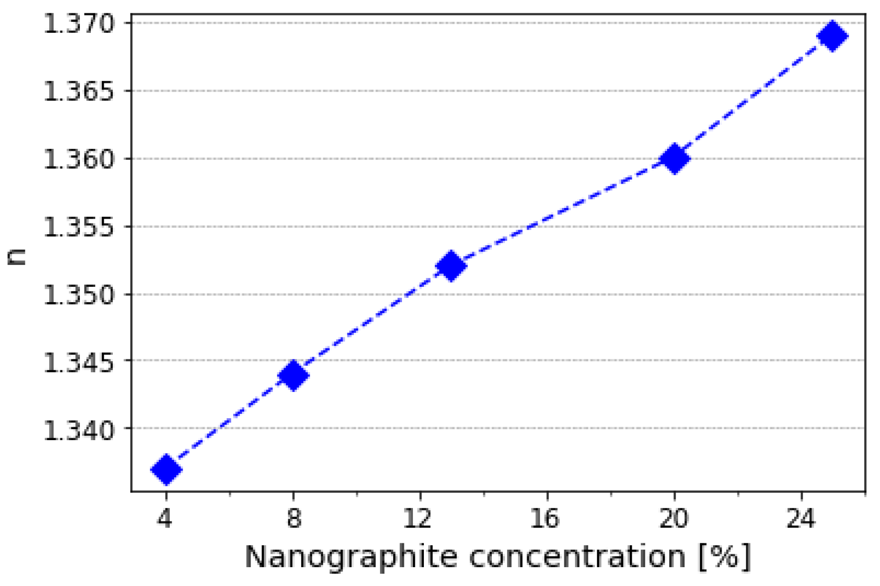
3.3. Optical Characterization

Prior to blade coating the nanographite films on the glass substrates, the refractive indexes of the nanographite suspension were measured with a digital refractometer, a Refracto 30PX. The precision of the refractometer is 0.0001, and the results were taken at 589.3 nm.
As expected from an aqueous solution, all nanographite suspensions presented refractive indices above 1.33. For a 4 % nanographite concentration, the refractive index range measured was 1.337. For a 25 % nanographite suspension, the refractive index increased to 1.369. The complete results are shown in Figure 10.
The nanographite flakes used to prepare the suspensions were analyzed according to their Raman spectrum (Figure 11) and X-ray diffraction (Figure 12).
Raman spectroscopy can provide valuable information with respect to the graphite quality once structural characteristics can be inferred from the spectrum. Considering single crystalline graphite, two Raman modes are expected: one at 42 cm−1, which is a low-frequency collective shear mode, and another one at 1585 cm−1, which is the characteristic G band [34]. As for the D band, first reported in 1970 [35] rising from the plane vibration, it shows the disorder modes that might be present in the nanographite sample.
In contrast to the G band, the D band is greatly affected by the laser energy [34]. At 488 nm, this mode is predicted at 1355 cm−1. Through increasing the excitation energy, the disorder band varies its position linearly in the Raman spectrum to greater wavenumbers and, simultaneously, decreases its amplitude until it completely disappears when the laser energy reaches 3.7 eV.
A sample of the nanographite flakes was analyzed via Raman spectroscopy. Raman data were collected with 30 mW power at 532 nm from 250 cm−1 to 1800 cm−1. For this reason, only the G and D bands are exhibited in Figure 11. Additional information regarding the Raman spectroscopy are provided as Supplementary Material.
Both the G and D band positions approximately agree with the results predicted in the literature. The G band is at 1570.15 cm−1, and the D band is at 1343.82 cm−1. Following the Tuinstra–Koening relation, the ratio between them, 0.12, led to a crystallite size of 160.21 nm.
From the ratio and the peak positions found, we can infer that the nanographite suspension used is highly ordered and there was no oxidation during its synthesis [36].
Two-theta X-ray diffraction was carried out at 1.5418 Å from 10° to 59° with a 0.02° step.
The [002] peak, clearly observed in the two-theta X-ray diffraction, is located at 26.667° as shown in Figure 12. Thus, the interplane distance between the nanographite flakes layers was calculated as 3.343 Å, as expected [37,38].
To evaluate whether any structural changes occurred in the nanographite flakes because of their processing into suspension and further deposition on the substrate via blade coating, the produced films (with three distinct nanographite concentrations: 8 % , 13 % , and 20 % ) were also submitted to X-ray diffraction.
Although the magnitudes of the diffraction patterns of the nanographite films are lower than those of the nanographite flakes, the intensities for the films tend to reach the peak from the nanographite flakes as the graphite concentration in the film increases. The presence of sodium silicate in the suspension did not significantly affect the graphite properties of the films once the interplane distance d 002 agreed with the one found from the nanographite flakes. However, its presence is noted via additional noise in the patterns. The results for three different nanographite concentrations in the films can be verified in Table 1.
The higher order reflections, d 100 , d 101 , and d 004 , were also studied and are in accordance with the state of the art for high-quality graphite. The d 100 and d 101 reflections for the graphite films were not intense enough to overcome the noise due to the lower graphite concentration and the presence of sodium silicate. As for the d 004 reflection peak, we noticed a small shift in the two-theta for the nanographite films: while the peak of the nanographite flakes was at 54.781°, the peak for the film moved 0.05° to the right.
Then, we verified the performance of the nanographite flakes, which were used as the base material, and it was found that the suspension itself did not undergo oxidation during any of the processes: synthesis of the suspension, blade coating, and thermal treatments. Their carbon structure was preserved throughout the whole process to disperse the nanographite flakes and further coat them on glass substrates. The post-fabrication heating processes did not damage or expand the graphite structure, and there was no impairment due to molecule adsorptions.
Another important aspect to analyze was the transparency of the nanographite films in the visible range. A high transmittance of a film that is also electrically conductive is a must in several industrial fields, such as photovoltaics.
Being able to tune the concentration of the nanographite in the suspensions, we anticipated that a compromise between the transparency in the visible range and the DC conductivity could be set for the analyzed nanographite films.
The transmittance value from 500 nm to 700 nm for the lowest graphite concentration films, 4 % and 8 % , was analyzed, as shown in Figure 13. As graphite is not transparent in the visible range, it was expected that the film manufactured with the lowest concentration of nanographite would give us the highest transparency. Therefore, two aspects were studied: the influences of the concentration of the nanographite and the thickness of the film.
With respect to the 4 % nanographite films, when varying the thickness from 406 nm to 1.55 µm, the transmittance decreased from an average of 70 % to 52 % , as no absorption peaks were present in this band. In comparison, with the 8 % nanographite film with a similar thickness of 1.63 µm, the transparency plummeted to 15 % . Recalling the surface coverage area data, Figure 3, there was a 98 % nanographite-coated area for an 8 % nanographite film against an 80 % covered area for the 4 % nanographite film.
Hence, increasing the film thickness via the coating parameters while maintaining the same nanographite concentration is less influential on the transparency than increasing the thickness by using a suspension with a higher concentration of nanographite. As a complementary advantage, taking into consideration the results in Figure 8, when the thickness of the film is increased, the resistance decreases, which means the DC electrical conductivity can be enhanced even with a compromise in the optical transparency.

4. Discussion

In this work, extensive research on blade-coated nanographite films on substrates was conducted. Conductive nanographite films were successfully fabricated and showed a high coverage (up to 99%) on surface areas of a few square centimeters. The process is scalable; hence, it can be extrapolated to coat even larger areas.
Through Raman spectroscopy and X-ray diffraction, the structural characteristics of the fabricated films and the high quality of the nanographite flakes were evaluated and showed no signs of either oxidation or expansion.
A relationship between the DC electrical conductivity and the transparency in the visible spectrum was shown, allowing the setting of a balanced performance of both properties of the films.
Additionally, this study revealed electrical anisotropy in the films due to the orientation of nanoflakes that was stimulated by the blade coating.
These results are promising, as they demonstrate an alternative method for manufacturing graphitic films, and different functionalities were explored. This technique, which has not yet been fully explored in thin-film research, is less expensive and complex compared to other established methods and allows for the satisfaction of industrial demands.
The fabricated films exhibit attractive functionalities in several fields, such as photonics and solar cells. They can also be integrated into lithography processes once they are resistant to immersion in common solvents and developers such as acetone and MIF300.

5. Patents

The graphite suspension developed in this work is under the patent BR 2024, BR10202400405, ‘Ultrathin graphitic film production process ultrathin graphitic films obtained therefrom’.

Supplementary Materials

The following supporting information can be downloaded at: https://www.mdpi.com/article/10.3390/micro4030029/s1.

Author Contributions

Conceptualization, S.V.G.N., P.E.S.P. and S.M.; methodology, S.V.G.N. and P.E.S.P.; formal analysis, P.E.S.P. and L.d.M.L.G.V.; investigation, P.E.S.P. and L.d.M.L.G.V.; resources, S.M. and H.E.H.-F.; data curation, L.d.M.L.G.V.; writing—original draft preparation, P.E.S.P.; writing—review and editing, S.V.G.N. and L.d.M.L.G.V.; supervision, S.M. and H.E.H.-F.; project administration, S.M.; funding acquisition, S.M. and H.E.H.-F. All authors have read and agreed to the published version of the manuscript.

Funding

This research was funded by National Council for Scientific and Technological Development, CNPq-NAMITEC, [grant numbers 406193/2022-3 and 407839/2023-2], and Coordination of Superior Level Staff Improvement, CAPES, [grant number 88887.705951/2022-00].

Data Availability Statement

All data from this research are available under request.

Acknowledgments

The authors acknowledge Nacional de Grafite for providing nanographite flakes samples. Also, the authors thank the technicians team at CCSNano, Lamult at IFGW-UNICAMP, and Central Analitica at IQ-UNICAMP.

Conflicts of Interest

The authors declare no conflicts of interest.

Abbreviations

The following abbreviations are used in this manuscript:
CVDChemical vapor deposition
GOGraphite oxide
SEMScanning electron microscopy
DCDirect current

References

  1. Geim, A.K.; Novoselov, K.S. The rise of graphene. Nat. Mater. 2007, 6, 183–191. [Google Scholar] [CrossRef]
  2. Partoens, B.; Peeters, F. From graphene to graphite: Electronic structure around the K point. Phys. Rev. B 2006, 74, 075404. [Google Scholar] [CrossRef]
  3. Jia, X.; Campos-Delgado, J.; Terrones, M.; Meunier, V.; Dresselhaus, M.S. Graphene edges: A review of their fabrication and characterization. Nanoscale 2011, 3, 86–95. [Google Scholar] [CrossRef]
  4. Novoselov, K.S.; Geim, A.K.; Morozov, S.V.; Jiang, D.E.; Zhang, Y.; Dubonos, S.V.; Grigorieva, I.V.; Firsov, A.A. Electric field effect in atomically thin carbon films. Science 2004, 306, 666–669. [Google Scholar] [CrossRef] [PubMed]
  5. Huang, Y.; Pan, Y.H.; Yang, R.; Bao, L.H.; Meng, L.; Luo, H.L.; Cai, Y.Q.; Liu, G.D.; Zhao, W.J.; Zhou, Z.; et al. Universal mechanical exfoliation of large-area 2D crystals. Nat. Commun. 2020, 11, 2453. [Google Scholar] [CrossRef]
  6. Obraztsov, A.; Obraztsova, E.; Tyurnina, A.; Zolotukhin, A. Chemical vapor deposition of thin graphite films of nanometer thickness. Carbon 2007, 45, 2017–2021. [Google Scholar] [CrossRef]
  7. Park, J.S.; Cho, S.M.; Kim, W.J.; Park, J.; Yoo, P.J. Fabrication of graphene thin films based on layer-by-layer self-assembly of functionalized graphene nanosheets. Acs Appl. Mater. Interfaces 2011, 3, 360–368. [Google Scholar] [CrossRef]
  8. Fredriksson, H.; Chakarov, D.; Kasemo, B. Patterning of highly oriented pyrolytic graphite and glassy carbon surfaces by nanolithography and oxygen plasma etching. Carbon 2009, 47, 1335–1342. [Google Scholar] [CrossRef]
  9. Adetayo, A.; Runsewe, D. Synthesis and fabrication of graphene and graphene oxide: A review. Open J. Compos. Mater. 2019, 9, 207. [Google Scholar] [CrossRef]
  10. Guo, Y.; Di, C.a.; Liu, H.; Zheng, J.; Zhang, L.; Yu, G.; Liu, Y. General route toward patterning of graphene oxide by a combination of wettability modulation and spin-coating. ACS Nano 2010, 4, 5749–5754. [Google Scholar] [CrossRef]
  11. Sumdani, M.; Islam, M.; Yahaya, A.; Safie, S. Recent advances of the graphite exfoliation processes and structural modification of graphene: A review. J. Nanoparticle Res. 2021, 23, 1–35. [Google Scholar] [CrossRef]
  12. Titelman, G.; Gelman, V.; Bron, S.; Khalfin, R.; Cohen, Y.; Bianco-Peled, H. Characteristics and microstructure of aqueous colloidal dispersions of graphite oxide. Carbon 2005, 43, 641–649. [Google Scholar] [CrossRef]
  13. Hummers, W.; Offeman, R. Graphite oxide (GO) was prepared using the well-known Hummers method described by Hummers. J. Am. Chem. Soc. 1958, 80, 1339–1345. [Google Scholar] [CrossRef]
  14. Hou, Y.; Lv, S.; Liu, L.; Liu, X. High-quality preparation of graphene oxide via the Hummers’ method: Understanding the roles of the intercalator, oxidant, and graphite particle size. Ceram. Int. 2020, 46, 2392–2402. [Google Scholar] [CrossRef]
  15. Botas, C.; Álvarez, P.; Blanco, P.; Granda, M.; Blanco, C.; Santamaría, R.; Romasanta, L.J.; Verdejo, R.; López-Manchado, M.A.; Menéndez, R. Graphene materials with different structures prepared from the same graphite by the Hummers and Brodie methods. Carbon 2013, 65, 156–164. [Google Scholar] [CrossRef]
  16. Sreeja, V.; Cheruvalathu, A.; Reshmi, R.; Anila, E.; Thomas, S.; Jayaraj, M. Effect of thickness on nonlinear absorption properties of graphite oxide thin films. Opt. Mater. 2016, 60, 450–455. [Google Scholar] [CrossRef]
  17. Karthick, R.; Brindha, M.; Selvaraj, M.; Ramu, S. Stable colloidal dispersion of functionalized reduced graphene oxide in aqueous medium for transparent conductive film. J. Colloid Interface Sci. 2013, 406, 69–74. [Google Scholar] [CrossRef]
  18. Patel, J.; Mighri, F.; Ajji, A.; Tiwari, D.; Chaudhuri, T.K. Spin-coating deposition of PbS and CdS thin films for solar cell application. Appl. Phys. A 2014, 117, 1791–1799. [Google Scholar] [CrossRef]
  19. Choi, J.S.; Lee, H.K.; An, S.J. Synthesis of a graphene oxide/sodium silicate nanocomposite using sodium silicate solution. RSC Adv. 2015, 5, 38742–38747. [Google Scholar] [CrossRef]
  20. Vaz, L.M.L.G.; Pellegrini, P.E.S.; Nista, S.V.G.; Moshkalev, S.; Figueroa, H.E.H. Ultrathin Graphitic Film Production Process and Ultrathin Graphitic Films Obtained Therefrom. BR Patent BR10202400405, 29 February 2024. [Google Scholar]
  21. Yang, H.; Jiang, P. Large-scale colloidal self-assembly by doctor blade coating. Langmuir 2010, 26, 13173–13182. [Google Scholar] [CrossRef]
  22. Butt, M.A. Thin-film coating methods: A successful marriage of high-quality and cost-effectiveness—A brief exploration. Coatings 2022, 12, 1115. [Google Scholar] [CrossRef]
  23. Dai, X.; Deng, Y.; Van Brackle, C.H.; Huang, J. Meniscus fabrication of halide perovskite thin films at high throughput for large area and low-cost solar panels. Int. J. Extrem. Manuf. 2019, 1, 022004. [Google Scholar] [CrossRef]
  24. Siegrist, S.; Nandi, P.; Kothandaraman, R.K.; Abdessalem, A.; Tiwari, A.N.; Fu, F. Understanding Coating Thickness and Uniformity of Blade-Coated SnO2 Electron Transport Layer for Scalable Perovskite Solar Cells. Solar RRL 2023, 7, 2300273. [Google Scholar] [CrossRef]
  25. Doumenc, F.; Salmon, J.B.; Guerrier, B. Modeling flow coating of colloidal dispersions in the evaporative regime: Prediction of deposit thickness. Langmuir 2016, 32, 13657–13668. [Google Scholar] [CrossRef] [PubMed]
  26. Mao, A.; Schaper, C.; Karlicek, R., Jr. Nanopatterning using a simple bi-layer lift-off process for the fabrication of a photonic crystal nanostructure. Nanotechnology 2013, 24, 085302. [Google Scholar] [CrossRef] [PubMed]
  27. Wolf, H.; Rawlings, C.; Mensch, P.; Hedrick, J.L.; Coady, D.J.; Duerig, U.; Knoll, A.W. Sub-20 nm silicon patterning and metal lift-off using thermal scanning probe lithography. J. Vac. Sci. Technol. B 2015, 33. [Google Scholar] [CrossRef]
  28. Abasahl, B.; Santschi, C.; Raziman, T.; Martin, O.J. Fabrication of plasmonic structures with well-controlled nanometric features: A comparison between lift-off and ion beam etching. Nanotechnology 2021, 32, 475202. [Google Scholar] [CrossRef] [PubMed]
  29. Miyazaki, H.; Odaka, S.; Sato, T.; Tanaka, S.; Goto, H.; Kanda, A.; Tsukagoshi, K.; Ootuka, Y.; Aoyagi, Y. Inter-layer screening length to electric field in thin graphite film. Appl. Phys. Express 2008, 1, 034007. [Google Scholar] [CrossRef]
  30. Galashev, A.E.; Rakhmanova, O.R. Mechanical and thermal stability of graphene and graphene-based materials. Physics-Uspekhi 2014, 57, 970. [Google Scholar] [CrossRef]
  31. Girotto, E.M.; Santos, I.A. Medidas de resistividade elétrica DC em sólidos: Como efetuálas corretamente. QuíMica Nova 2002, 25, 639–647. [Google Scholar] [CrossRef]
  32. van der Pauw, L.J. A method of measuring the resistivity and Hall coefficient on lamellae of arbitrary shape. Philips Tech. Rev. 1958, 20, 220–224. [Google Scholar]
  33. Darabut, A.M.; Lobko, Y.; Yakovlev, Y.; Rodríguez, M.G.; Veltruská, K.; Šmíd, B.; Kúš, P.; Nováková, J.; Dopita, M.; Vorokhta, M.; et al. Influence of thermal treatment on the structure and electrical conductivity of thermally expanded graphite. Adv. Powder Technol. 2022, 33, 103884. [Google Scholar] [CrossRef]
  34. Pócsik, I.; Hundhausen, M.; Koós, M.; Ley, L. Origin of the D peak in the Raman spectrum of microcrystalline graphite. J. Non Cryst. Solids 1998, 227, 1083–1086. [Google Scholar] [CrossRef]
  35. Tuinstra, F.; Koenig, J.L. Raman spectrum of graphite. J. Chem. Phys. 1970, 53, 1126–1130. [Google Scholar] [CrossRef]
  36. Kudin, K.N.; Ozbas, B.; Schniepp, H.C.; Prud’Homme, R.K.; Aksay, I.A.; Car, R. Raman spectra of graphite oxide and functionalized graphene sheets. Nano Lett. 2008, 8, 36–41. [Google Scholar] [CrossRef] [PubMed]
  37. Popova, A. Crystallographic analysis of graphite by X-ray diffraction. Coke Chem. 2017, 60, 361–365. [Google Scholar] [CrossRef]
  38. Wang, G.; Yang, J.; Park, J.; Gou, X.; Wang, B.; Liu, H.; Yao, J. Facile synthesis and characterization of graphene nanosheets. J. Phys. Chem. C 2008, 112, 8192–8195. [Google Scholar] [CrossRef]
Figure 1. Illustration of nanographite film deposition via blade coating. The deposition direction is indicated by the velocity v . The thickness of the films in both wet and dry regimes is denoted by t w e t and t d r y , respectively.
Micro 04 00029 g001
Figure 2. (a,b) An 8 % and 25% nanographite film produced via blade coating, respectively. The insets highlight the difference in transparency between them. (cf) SEM images of films with 4%, 8%, 13%, and 25% of nanographite, respectively. The scale bar is 50 μm.
Micro 04 00029 g002
Figure 3. Coated surface area of a glass substrate after blade coating the nanographite suspension from 4 % to 25 % of graphite.
Micro 04 00029 g003
Figure 4. Linear relationship between the thickness of the nanographite films and the volume of the solution deposited via blade coating. The concentration of graphite varied from 4 % to 25 % . The markers are the experimental measurements, while the solid lines are the linear regressions.
Micro 04 00029 g004
Figure 5. The thickness of the films against the nanographite concentration in the solution for 8 µL, 18 µL, and 28 µL of solution deposited. The markers indicate the experimental data, and the solid lines indicate the exponential fittings.
Micro 04 00029 g005
Figure 6. Comparison of the film thicknesses for 25 % nanographite solution using different blades (beveled at 45° and cylindrical).
Micro 04 00029 g006
Figure 7. Comparison of the resistances with and without thermal treatment at 350 °C, for 13%, 20%, and 25% nanographite films.
Micro 04 00029 g007
Figure 8. Resistance measured using the four probe method for 13%, 20%, and 25% nanographite films. Measurements labeled ‖ are parallel to the coating direction, and ⊥ are perpendicular.
Micro 04 00029 g008
Figure 9. Electrical conductivity of nanographite films with concentrations varying from 8% to 25%. Resistances taken parallel to the flakes’ orientation were considered.
Micro 04 00029 g009
Figure 10. Refractive index of the nanographite suspension, varying the graphite concentration from 4% to 25%. Measurements were taken at 589.3 nm.
Micro 04 00029 g010
Figure 11. Raman spectroscopy of the nanographite flakes used in the suspensions.
Micro 04 00029 g011
Figure 12. (a) The X-ray diffraction pattern for the nanographite flakes. (b) The patterns obtained for the nanographite films and a pure sodium silicate film.
Micro 04 00029 g012
Figure 13. Transmittance of nanographite films at 4 % and 8 % from 500 nm to 700 nm.
Micro 04 00029 g013
Table 1. The interplane distance in nanographite films at different concentrations.
Concentration of Nanographite in Film [ % ] d 002 [Å]
83.333
133.333
203.335
Disclaimer/Publisher’s Note: The statements, opinions and data contained in all publications are solely those of the individual author(s) and contributor(s) and not of MDPI and/or the editor(s). MDPI and/or the editor(s) disclaim responsibility for any injury to people or property resulting from any ideas, methods, instructions or products referred to in the content.

