Review

Differential Hall Effect Metrology for Electrical Characterization of Advanced Semiconductor Layers

Active Layer Parametrics (ALP), 5500 Butler Lane, Scott Valley, CA 95066, USA
*
Author to whom correspondence should be addressed.
Metrology 2024, 4(4), 547-565; https://doi.org/10.3390/metrology4040034
Submission received: 14 August 2024 / Revised: 18 September 2024 / Accepted: 30 September 2024 / Published: 2 October 2024

Abstract

:
Semiconductor layers employed in fabricating advanced node devices are becoming thinner and their electrical properties are diverging from those established for highly crystalline standards. Since these properties also change as a function of depth within the film, accurate carrier profiling solutions are required. The Differential Hall Effect (DHE) technique has the unique capability of measuring mobility and carrier concentration (active carriers) through the depth of a semiconductor film. It comprises making successive sheet resistance and sheet Hall coefficient measurements as the thickness of the electrically active layer at a test region is reduced through successive material removal steps. Difference equations are then used to process the data and plot the desired depth profiles. The fundamentals of DHE were established in 1960s. Recently, the adaption of electrochemical processing for the material removal steps, and the integration of all other functionalities in a Differential Hall Effect Metrology (DHEM) tool, has made this technique more practical and accurate and improved its depth resolution to a sub-nm range. In this contribution, we review the development history of this important technique and present data from recent characterization work carried out on Si, Ge and SiGe layers.

1. Introduction

The development of next-generation semiconductor technologies comes with escalated costs due to ever-increasing technical challenges and extended development cycles needed to meet such challenges. Dependable, high-resolution electrical characterization techniques are key for efficient film/device development efforts. Traditional methods, such as four-point probe (4PP) and the Hall effect measurements performed on bulk films, are not adequate to characterize the semiconductor layers with electrical properties varying as a function of depth. Relying on 4PP and Hall effect measurements, which provide average resistivity and effective mobility values, can be quite misleading in some cases.
Recognition of the benefits of measuring electrical parameters as a function of depth through a semiconductor film gave rise to the development of techniques such as Spreading Resistance Profiling (SRP) [1,2,3], Scanning Spreading Resistance Microscopy (SSRM) [4,5,6,7,8], Electrochemical Capacitance-Voltage (E-CV) measurement [9,10,11,12] and Scanning Capacitance Microscopy (SCM) [13,14,15,16]. A series of micro 4PP resistivity measurements along a beveled sample with a bevel angle of a few minutes was also used to obtain carrier depth profiles [17,18]. SSRM and SRP approaches require sample sectioning or angle lapping, and they measure spreading resistance under point contacts traveling on the sectioned or lapped edge of the sample. The spreading resistance profile is turned into resistivity using established models while taking account other factors such as carrier spilling [5], probe penetration [19], bias-induced effects [20] and measurement environment [21]. E-CV, on the other hand, measures carrier concentration (active dopants) directly and is very sensitive to the exact definition of the measurement area. One important limitation of these approaches is the fact that they do not directly measure mobility as a function of depth. SRP and SSRM derive mobility values from established standards and calibration samples. Then, corrections may be introduced to the raw data to eliminate some of the effects mentioned before. The silicon mobility models are based on a 1981 publication [22], while the germanium models are mostly taken from a 1961 paper [23]. These models, which were established using high-quality bulk crystalline materials, may not fully represent the materials produced today using modern thin film processes such as atomic layer deposition, advanced doped epitaxial growth and non-equilibrium annealing, such as laser annealing, etc. For the transistor source/drain (S/R) contact regions, for example, heavily doped materials such as boron (B)-doped silicon-germanium (SiGe) and Si-phosphorus (P) alloys are being developed. Standard mobility models of the past may not be able to consider the presence of defects and excessive scattering due to super doping and could overestimate the mobility values. This, in turn, would underestimate the calculated active dopant concentration. Models also do not directly expand to include new materials, such as SiGe alloys with varying amounts of Ge. Therefore, standards have been developed to measure them. There are also limited electrical data regarding thin films of III-V materials grown by different approaches. A commonly used depth profiling technique, secondary ion mass spectrometry (SIMS), measures doping profiles through semiconductor layers. These profiles provide the concentration of the dopants in the material. What is important for devices, however, is the distribution of the electrically active fraction of the dopants. Therefore, a technique that can directly measure depth profiles of mobility and carrier concentration through layers at high-depth resolutions is valuable. The Differential Hall Effect measurement is such a technique.

2. Hall Effect

The Hall effect was discovered over 140 years ago [24]. Its principle states that a transverse voltage is developed in a conductor slab carrying an electric current when the conductor is placed in a magnetic field that is perpendicular to the direction of the current flow. The traverse voltage developed is called the Hall voltage (VH) and is related to the current and the magnetic field through the relationship:
VH = (RH I B)/t
where I is the current, B is the magnetic field strength, t is the thickness of the slab and RH is the Hall coefficient defined as:
RH = r/Ne = rµρ = μH ρ
where r is the Hall scattering factor for the material, N is the dominant carrier concentration, e is the elementary charge, µ is the conductivity mobility, ρ is the resistivity and µH is the Hall mobility. A sketch demonstrating the Hall effect is shown in Figure 1.
As can be seen from Equations (1) and (2), if the current conducting material has uniform electrical properties, measurement of sheet resistance (ρ/t) and Hall voltage would yield a Hall mobility value, which can be converted into conductivity mobility by dividing with the Hall scattering factor, r. In knowing the sheet resistance, the thickness and the conductivity mobility values, one can then calculate the carrier concentration, N.
Hall effect measurements have been commonly employed to determine the bulk mobility and carrier concentration in semiconductor layers with uniform electrical properties [25]. The theoretical foundation of Hall data evaluation for irregularly shaped samples was developed by van der Pauw [26,27]. Simplified equations based on van der Pauw (VdP) formulations are typically used for symmetric samples with shapes such as circles, squares, cloverleaves and crosses [28]. Therefore, Hall effect measurements are relatively simple to interpret for uniformly doped samples. However, if the carrier concentration and the mobility values vary in the z direction, the Hall effect measurements yield average or effective resistivity, carrier density, and mobility data that become very difficult to interpret [29].
Petritz formulated the problem of determining the carrier concentration and mobility within a surface depletion region of a semiconductor layer using conductivity and Hall effect measurements [30]. He treated the film as a two-layer structure comprising a surface layer with thickness t1, Hall coefficient RH1 and conductivity σ1, as well as a bottom layer with a different set of values (t2, RH2, σ2) for these variables. Through modeling, he showed that the overall Hall coefficient RH measured for such a film with total thickness, t, would be a complex function (as shown in Equation (3)). He also showed that one can calculate the electrical properties of the surface layer by utilizing the Hall effect and conductivity measurements as a function of the applied surface potential, which changed the surface depletion width (t1 in Equation (3)).
RH = t (RH1 σ12 t1 + RH2 σ22 t2)/(σ1 t1 + σ2 t2)2
An extension of Petritz’s formulation to a film with the carrier concentration, N(z), and mobility, µ(z), changing continuously in the z direction yields the following equation for the effective Hall mobility value, μH eff, that would be measured in a Hall effect experiment:
μH eff = r µeff = r [∫ n(z) μ(z)2 dz]/[∫ n(z) μ(z) dz]
As can be seen from Equation (4), a high-mobility region in a non-uniform film may contribute more to the overall value of the measured Hall mobility because of the μ(z)2 factor. The carrier concentration calculated from this effective Hall mobility value would also be biased. Depending on how the mobility and the carrier concentration may vary through the thickness of the film, the bulk effective values measured cannot represent the true character of the film and, therefore, can be very misleading. Equation (4) above assumed a constant r value. However, the situation becomes more complex if r is also varying in the z direction. SiGe-stacked layers with changing Ge content in the z direction is an example of this case.

3. Differential Hall Effect (DHE)

Modern day devices employ semiconductor layers with highly non-uniform electrical properties. Doping and annealing procedures often yield films with active dopant concentration and mobility values changing greatly through the film thickness. The DHE method was devised to electrically characterize such films and provide depth profiles for the mobility and carrier concentrations. The technique involves successive surface layer removal and electrical measurement steps, wherein the surface layer removal steps continually thin down the electrically active sample under study and the electrical measurement steps yield sheet resistance/conductance and Hall effect data after each thinning step. Information collected this way can then be used in differential relationships to derive the electrical property depth profiles.

3.1. Early Work on Differential Conductivity Measurements

Measuring the conductivity of a film, removing a thin surface region, re-measuring the conductivity of the remaining portion of the film, and repeating these steps several times was a method employed by researchers to determine a depth profile of the conductivity of the sample [31,32,33,34,35]. The data obtained were typically interpreted to determine the carrier profiles using the standard resistivity vs. carrier density relationships [21,22]. Material removal was usually achieved through mechanical polishing. Removed thickness determination, which is needed in the calculations, typically involved weighing the sample before and after the polishing step. Obviously, this technique could only be used for relatively thick (several micrometers) samples, and it offered only limited depth resolution. Tannenbaum introduced the idea of using anodic oxidation followed by hydrogen fluoride (HF) etching for better-controlled surface layer removal of Si [31]. In this approach, she used calibrated charts of oxide color versus thickness to determine the anodic oxide thickness and then converted it into Si thickness removed. Davies et al. also used this anodization/stripping method for a different purpose, and they calibrated the material removal rate using neutron activation analyses [36].
As can be seen from the review above, the differential conductivity studies did not include mobility measurements. However, anodic oxidation was shown to be a viable method to remove surface layers of controlled thickness from Si samples.

3.2. Early Work on DHE

Combining material removal and the Hall effect in a measurement was proposed by Subashchiev et al., who implemented it to determine the carrier density and the mobility in the surface layer of an Si sample after a dopant diffusion process [37]. In this work, the Hall effect and resistivity measurements were carried out before and after the surface of the sample was etched, and the data were interpreted to derive the carrier concentration and mobility within the etched section of the surface. The removed-material thickness in that work was determined by weighing the sample before and after the etching step. Buehler extended this approach to the determination of electrical property depth profiles through III–V compound layers [38]. He formulated and used a Hall 4PP technique to determine the resistivity and sheet Hall coefficient values for circular samples before and after successive thinning steps. Material removal was achieved through lapping. A series of approximately 10µm thick surface layers were removed during each step and the removed-material thickness was determined by weighing the sample before and after thinning. The collected data were used to plot the carrier density and resistivity as a function of depth. Mayer et al. employed a more standard Hall effect measurement approach with clover leaf-shaped VdP patterns in their experiments to study ion-implanted Si wafers [39]. Through sheet resistance and Hall voltage measurements, coupled with anodic oxidation/HF etching steps, they were able to obtain electrical property depth profiles with a depth resolution of ~15–50 nm. The amount of Si removed in their experiments was determined from differential weight measurements or multiple-beam interferometry. Mayer’s approach was later used by others to study the behavior of various dopants introduced in Group IV materials [40,41,42,43,44,45] and Group III-V compounds [46,47,48,49,50]. The difference equations used to calculate the Hall mobility and carrier concentration values in these studies were as follows:
µHi = i = [(RHs σs2)i+1 − (RHs σs2)i]/[(σs)i+1 − (σs)i]
Ni = [(σs)i+1 − (σs)i ]/(e Δz µi)
where, “i” refers to measurements made before the ith layer is removed and “i + 1” refers to measurements made after the ith layer is removed. µHi, µi, Ni and Δz are the Hall mobility, the conductivity mobility, the carrier concentration and the thickness of the removed layer, respectively. RHs is the measured sheet Hall coefficient, σs is the measured sheet conductance, e is the elementary charge and r is the Hall scattering factor. The derivation of these equations and the measurement procedure was described by Buehler [38] and Mayer et al. [39].
As can be seen from Equations (5) and (6), one needs the values of r and Δz to be able to calculate and plot an accurate carrier concentration depth profile. It is very common in the literature to assume r = 1. This may work for some materials; however, it may introduce large errors for others. Determining Δz values accurately is needed in the calculations and also defines the depth resolution that can be achieved by the measurement. As we have seen above, depth resolution for early DHE measurements were, at best, in the 15 nm range because of the limitations of the material removal techniques and the uncertainties in Δz measurements. The best material removal approach for Si was found to be an anodic oxidation (anodization) step that grew an oxide film over the sample, followed by an etching step in HF. The thickness of the Si removed through this process was determined through various means including differential weight measurements and measuring the etched step height by interference microscopy. In some approaches, the thickness of the anodic oxide was determined through ellipsometry or by using color calibration charts. The oxide thickness found was then converted into Si thickness removed, which is approximately half of the oxide thickness. Some publications reported computer algorithms developed to smoothen the DHE depth profiles and to analyze the data more efficiently [51,52].
As the above review shows, early DHE measurements were manual, tedious and time consuming. Hall effect/VdP evaluations providing the conductivity and mobility information were made at one measurement station and the material removal steps were carried out at a separate station under a chemical hood. This meant that, for example, a multi-step measurement through a film required several trips between these stations. Measurement of the material thickness removed was typically performed after multiple thinning steps which yielded an average “per step” removal rate. Electrical contacts had to be removed from the sample surface after each measurement step and then re-placed after the etching step. Making and breaking contacts tens of times ran the risk of degrading the contact areas and/or the junction underneath, especially for thin samples. This increased measurement noise and negatively impacted the data.
Efforts geared towards making DHE a more accurate and user-friendly technique included developing designs to reduce contact noise problems, formulating ways to determine the removed-material thickness without ex situ measurements and increasing throughput through automation. In this respect, one important development was the recognition of the possibility of estimating the Si-oxide thickness from the value of the applied anodization potential in properly formulated electrolytes. Barber et al. reported that the average thickness of Si removed in their anodization process was 2.21 Å/V. This meant that a depth resolution of about 0.2 nm would be possible for Si measurements. Although these researchers applied their findings only to differential conductivity measurements, they pointed out their potential use in DHE measurements [53].
Another important development was the design of sample holders in the form of electrolytic cells, which allowed the anodization, etching, rinsing and drying processes to be carried out in situ [54,55]. These cells could also be placed between the poles of electromagnets so that Hall effect measurements could be carried out after each etching/rinsing/drying step. The anodization solution, HF etchant, deionized (DI) water and drying nitrogen were injected into the cell during the anodization, etching, rinsing and drying steps, respectively. Electrical contacts were outside the process region and were stationary during all the steps, including the measurement steps. This reduced the contact noise. A version of such equipment with the capability of carrying out measurements at liquid nitrogen temperatures was also designed [56].
Efforts to automate the DHE process included mechanical designs that moved the sample by a carrier between beakers containing the anodization solution, the HF solution and DI water. The carrier had a circular or linear motion and had also the capability of bringing the sample in front of a nitrogen drier before electrical measurements and in between the poles of a magnet for Hall effect data collection [57,58].
Alzanki et al. reported DHE measurement results on ultra-shallow Si junctions with junction depths in the range of 20 nm [59,60,61]. To be able to provide enough numbers for the data points through these thin films, the depth resolution had to be improved. These researchers developed a native oxide growth and strip process which involved immersing the sample into DI water for a few seconds that grew an oxide film over the surface. After rinsing and drying, Hall effect measurements were carried out, and then the thin oxide layer was etched in HF solution, preparing the sample for the next cycle. After multiple oxidation/measurement/etching steps, the total etched depth was measured by a profilometer. Using this total value, the etched depth per step was found to be ~2 nm. This way, authors studied electrical activation depth profiles of antimony (Sb) dopant in Si as a function of the annealing temperature. A similar approach was employed by Bennett et al., who studied B and Sb activation in Si and reported an appreciable dependence of the material removal rate on dopant species [62]. A comparison of B- and Sb-implanted material showed that the Sb-doped Si etch rate was about nine times larger than the B-doped Si. In a later publication, Sb- and arsenic (As)-doped materials were shown to have similar etch rates in this native oxide growth and strip process [63].
SiGe alloys are important for optimization of source/drain (S/D) contact resistivity in advanced node transistors. S/D junction regions in such devices are ultra-shallow, and thus the depth resolution of the profiling approach needs to be high. Application of the native oxide growth and strip process to SiGe alloys was very challenging due to the different oxidation rates of the two species. Therefore, a chemical etching technique was investigated for this application instead of the native oxide growth and strip approach. Daubriac et al. developed an SiGe chemical etching process with an etch rate of ~0.1 nm/min [64,65]. They, however, also found that the etch rate varied with the Ge content of the alloy for etch times longer than 15 min.

4. Differential Hall Effect Metrology (DHEM)

The DHE technique is unique among other electrical depth profiling approaches in that it provides direct mobility measurements as a function of depth through a semiconductor film. This way, accurate carrier concentration profiles can be determined if the material removal rate can be well regulated and controlled. As reviewed above, early DHE methods had certain shortcomings. They were labor-intensive, tedious and slow techniques. They had the problems of poor prediction and repeatability of the material removal rates and a lack of access to an integrated/automated tool performing all process steps in situ.
To address the low throughput issue, some simple tool designs were suggested; however, they were not adequate. Use of native oxide formation and stripping technique improved the depth resolution to a few nanometers, but this approach did not offer a predictable material removal rate for Si since it was influenced by the nature of the surface and the type of the dopants. Also, this approach was not applicable to Ge and SiGe. All these early approaches also involved multiple HF etching steps followed by rinsing and drying.
An important advance in bringing the differential Hall Effect technique closer to practicality came when it was recognized that the oxide formed on the surface would insulate the semiconductor underneath from the conductive electrolyte and, therefore, the entire series of oxidations and electrical measurements could be carried out continually without any HF etching as the oxide layer grew thicker during each anodization step [66,67]. The method was called the Continuous Anodic Oxidation Technique (CAOT) and allowed for a certain degree of process automation, resulting in increased throughput. This approach was implemented on semi-automated desktop equipment and was successfully used to analyze doped Si structures and ultra-shallow junctions to demonstrate its feasibility [68,69,70,71]. Qin et al. used the technique to compare profile results from SIMS and SRP on B-doped (beam-line ion implant, plasma doping-PLAD) Si samples [72]. Authors concluded that the CAOT method achieved more reasonable data compared to SRP. Several papers were published on the optimization of dopant implants and annealing steps for high dopant activation using the CAOT [73,74,75]. Technology was transferred into an integrated automatic tool (ALProTM) and was renamed Differential Hall Effect Metrology (DHEM).
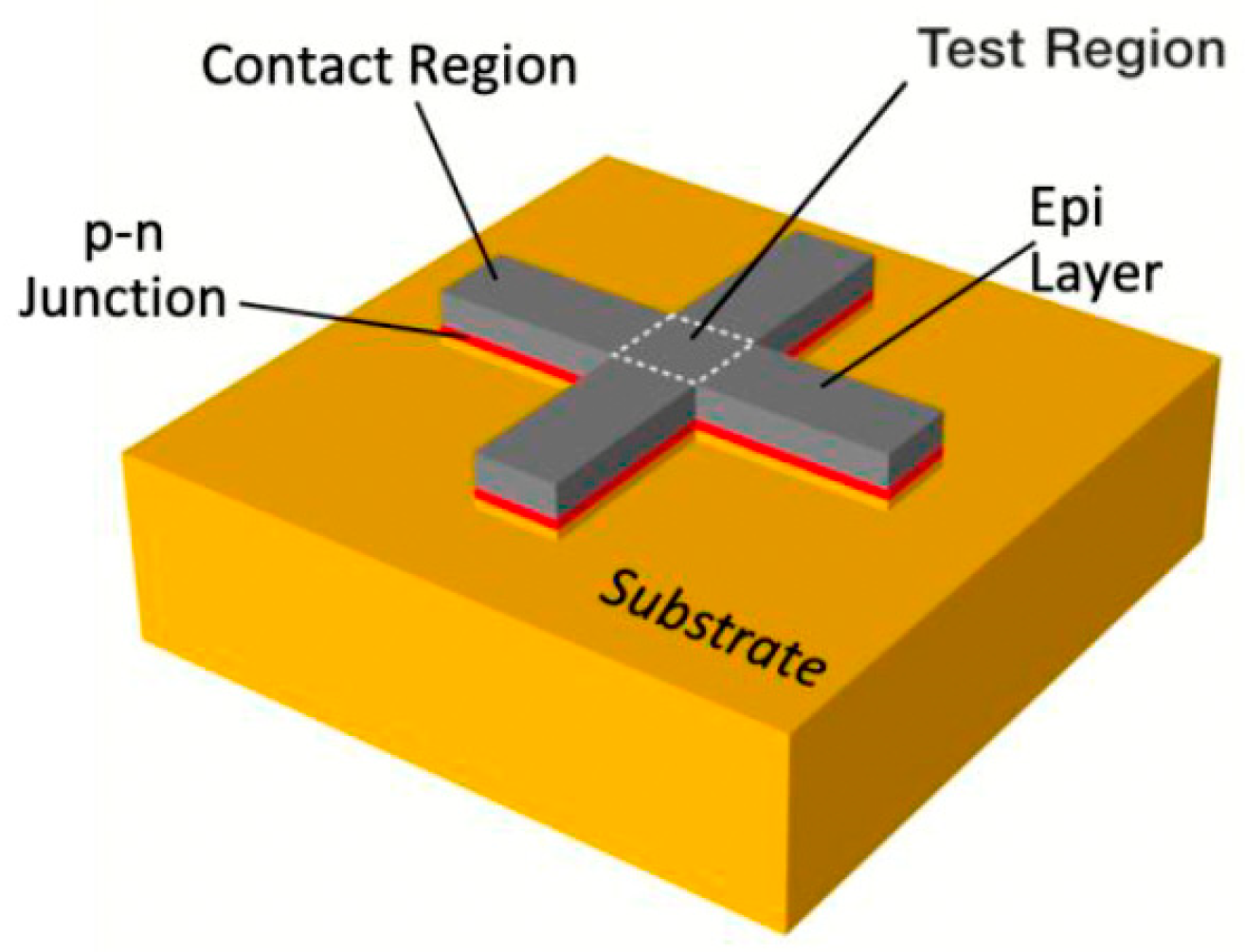
In a DHEM measurement, a test pattern, such as a VdP cross, is prepared on the coupon sample to be characterized [76,77]. A photolithography/dry etch approach is typically used for this purpose. The resulting cross has a mesa structure isolating the top film to be characterized from its surroundings, as can be seen in Figure 2. It is also important that there is an insulating barrier electrically separating the top film from the substrate below to avoid interference from the substrate. The insulating barrier may be an oxide layer or a p-n junction (i.e., the film to be characterized may be an n-type film formed over a p-type substrate, or vice versa). There are four electrical contact regions at the ends of the cross arms and a test region at the center of the cross where the arms intersect. The size of the test region can typically be adjusted from 0.5 mm × 0.5 mm to 2 mm × 2 mm so that the data collected are representative of that area of the sample.
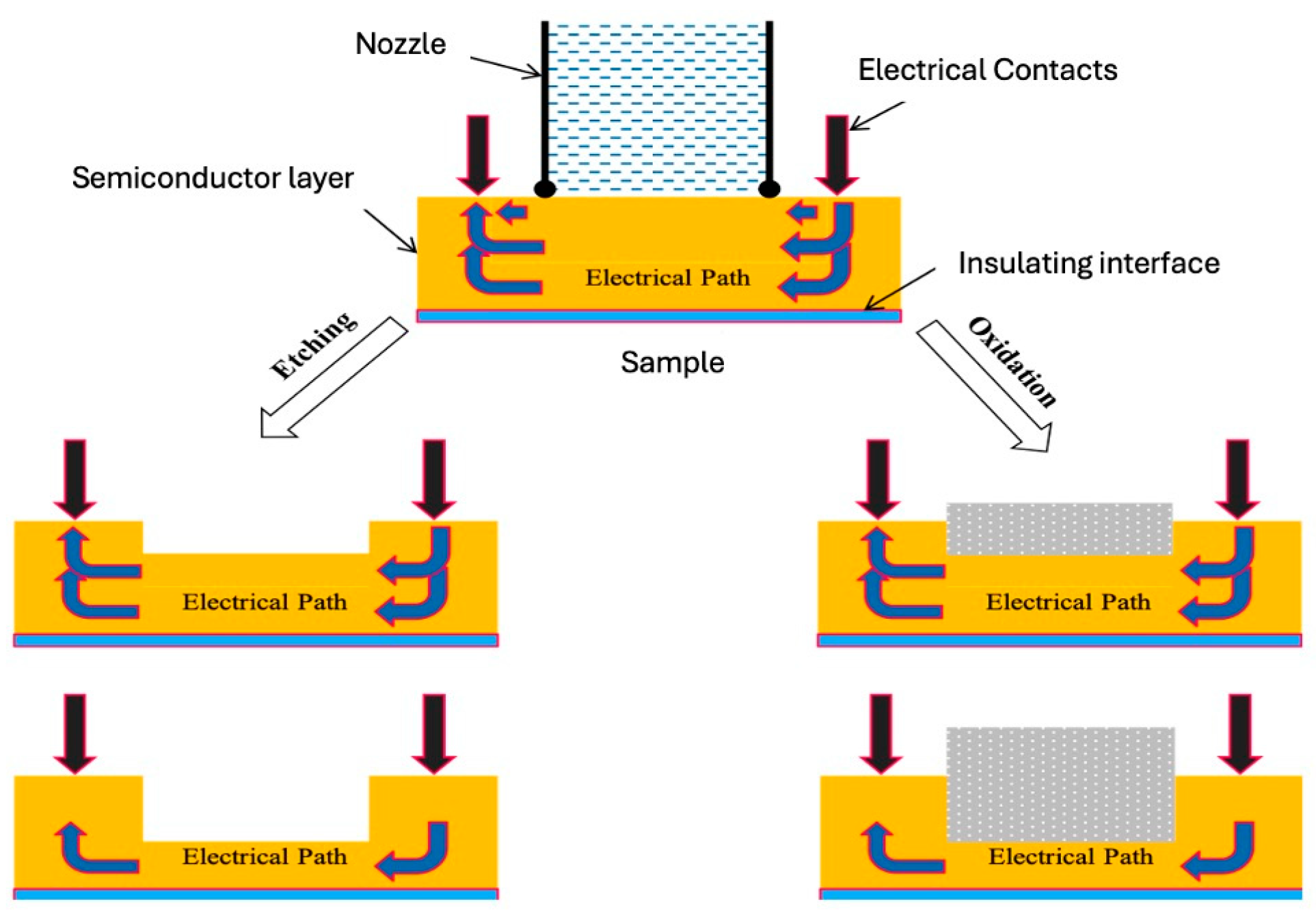
The first step in the process is to carry out bulk sheet resistance and Hall measurements using the test pattern of Figure 2 and the well-known standard procedures [28]. Four electrical contacts are applied to the four contact regions for these measurements. The nozzle of a mini process chamber is then lowered onto the sample and sealed against an area including the test region. The mini process chamber comprises an inert electrode. The nozzle has the capability of delivering chemical solutions, DI water or nitrogen gas to the test region. Figure 3 shows a cross-sectional sketch of the electrical contact and nozzle positions over the test region.
Once the nozzle is in place, a specially formulated solution is delivered to the surface of the test region for the material-thinning step. There are two options for reducing the electrically active thickness of the layer at the test region in a stepwise manner by applying an anodic voltage to the sample with respect to the electrode. One way is electro-etching the material to create a trench (left side of Figure 3). This approach is used for materials, such as Ge, that do not form stable oxides in the solution. The other way is to convert a thin slice of the material into an insulating oxide (right side of Figure 3). This approach is used for Si and for SiGe compositions that form stable oxides. In either case, measurements of the sheet resistance and sheet Hall coefficient are carried out after each thickness reduction step utilizing the Hall effect/VdP techniques. During Hall effect measurements, a magnet is automatically moved to underneath the sample. The collected data are then processed using Equations (5) and (6) and the depth profiles of the mobility and carrier concentrations are obtained.
It should be noted that all the material thinning and measurement steps of DHEM are carried out in situ without taking the sample out of the tool. Therefore, a fast turnaround (30 min to 2 h) is possible depending on the depth resolution, the number of data points at each step, and the depth range desired. Certain criteria must be met to obtain the best depth resolution and the most accurate data from DHEM measurements, i.e., (i) the material removal step must remove a sub-nm thick sheet of the surface region of the sample in a uniform manner from the whole test region, (ii) the electrochemical processes used should not increase the surface roughness and (iii) the removal rate should be predictable, controllable and repeatable [78].
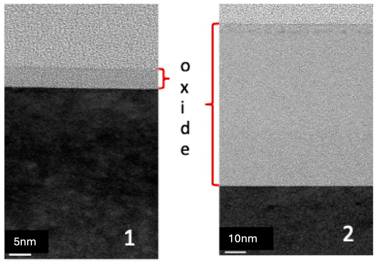
Electro-etching and anodic oxide formation approaches used in the DHEM technique satisfy the above listed criteria. From Faraday’s law, one can calculate that, for 1 cm2 area of a Ge anode, for example, one would remove about 3.5 × 10⁻⁴ Å of material upon passing 1 µC of charge assuming all charge is used to form Ge4+. In practice, some of the charge is used for side reactions. Still, the theoretical calculations show that electro-etching would offer the required sub-nanometer range removal control, provided that the electrochemical cell (mini chamber + nozzle) is designed to assure tight control of the etched area, uniform etching within that area and tight control of the etching current in the µA range. In our experiments, we found a repeatable depth resolution of about 4 Å for Ge measurements. As for the insoluble anodic oxide film formation for Si and SiGe, a linear relationship exists between the thickness of the oxide formed and the anodic voltage across the oxide. Therefore, oxide thickness can be easily predicted without moving the sample out of the tool for measurements. A typical calibrated anodization process can yield an oxide formation rate of about 4 Å/V. Since each 1 Å of SiO2 is formed by consuming ~0.5 Å of Si, DHEM has the capability of offering a depth resolution in the 2 Å range for Si. This means the technique can remove about one atomic layer of Si at each anodic oxidation step. The nanometer range depth resolution was reported previously by the native oxide growth and strip process. However, as discussed before, the repeatability of that approach was not adequate and there was a need to etch the oxide after each step. Use of an electrochemical approach eliminates the chemical etching steps while offering good thickness control for the oxidized surface of the semiconductor. Figure 4 shows the transmission electron microscopy (TEM) cross-sections taken after two different anodic oxidation steps applied to the same sample [79]. Sample #1 was oxidized at an oxidation potential of 13 V, and the potential for sample #2 was 195 V. TEM data show an oxide thickness of ~5 nm and ~75 nm for the two samples. This indicates an oxide formation rate of about 4Å/V for both cases and demonstrates the excellent oxide thickness control possible with the technique. In experiments where the Si substrates were anodized under the same conditions, we found the oxide thickness produced to be within 10% of the value measured by TEM, which has a similar measurement accuracy. This suggests that the accuracy of the depth scale provided by a DHEM profile is also within 10% of the real value.
As for the uniformity question, anodic oxide formation is intrinsically a very uniform process, since the oxide film grown has much higher resistance than the process solution. Furthermore, the magnitude of the ionic current that forms the oxide depends exponentially on the oxide thickness. If the oxide thickness was low at a location, the current density at that location would momentarily increase and repair the non-uniformity. Also, DHEM electro-etching and oxidation processes were found not to increase the surface roughness of Ge, Si and SiGe samples [78].

5. Recent DHEM Application Examples

DHEM can be viewed as an “electrical version of SIMS”. It provides depth profiles of active dopants through semiconductor films and thus can be used in any application where knowledge of activation is important and where activation may vary with depth within the film. Comparing the SIMS compositional data (total dopants) with DHEM electrical data (active dopants) obtained from the same layer is especially powerful for establishing a correlation between the electrical quality of the layer and the film growth/doping/annealing processes.
DHEM is a destructive technique, just like SIMS, SRP, ECV and SSRM. Being an electrical characterization approach, DHEM requires samples with a certain configuration (see Figure 2 and Section 6). These restrictions do not exist for a composition measuring technique such as SIMS. Extension of DHEM to a new material (other than Ge, Si and SiGe) would require development of an electrolyte appropriate for that material and calibration of the material removal rate with respect to the applied voltage in that new electrolyte.
Some of the application areas of DHEM include optimization of dopant deposition and activation (ion implantation, plasma doping, rapid thermal processing-RTP/laser/flash annealing, etc.), epi layer optimization (sheet resistance, mobility, carriers as a function of depth and process variables) and composition/defectivity/stress/mobility correlation through layers. Below, we will review some of the recent representative examples of DHEM studies.
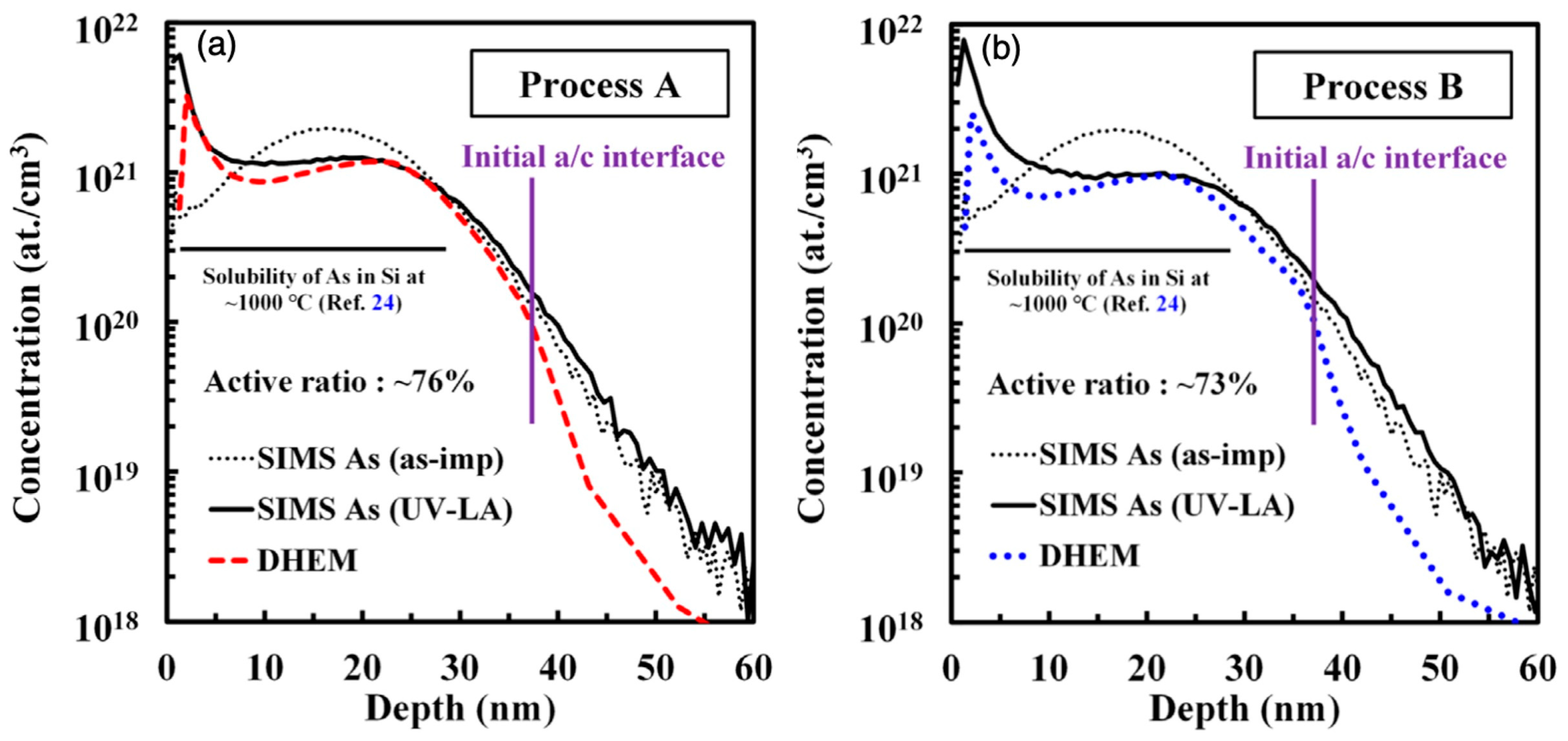
UV laser annealing (UV-LA) strongly limits vertical heat diffusion and therefore is an important process in dopant activation for three-dimensional CMOS technology. Figure 5 shows the result of a study on the µsec UV-LA process carried out on an As ion-implanted Si-on-insulator substrate [80]. The Si layer over the insulator was 70 nm thick and the top 37 nm was amorphized during As implantation. Two samples were processed by UV-LA under two different time–temperature profiles, with the ultimate temperature being close to 1000 °C (Process A and Process B). DHEM was used to evaluate carrier concentration profiles under the two conditions. As can be seen from the data in Figure 5, DHEM was able to resolve the subtle differences in the carrier concentration profiles of the two samples processed differently. Activation was found to be higher for Process A. Near-surface carrier concentrations of >1021 cm−3 were achieved which were much higher than the reported solubility limit of As in Si.
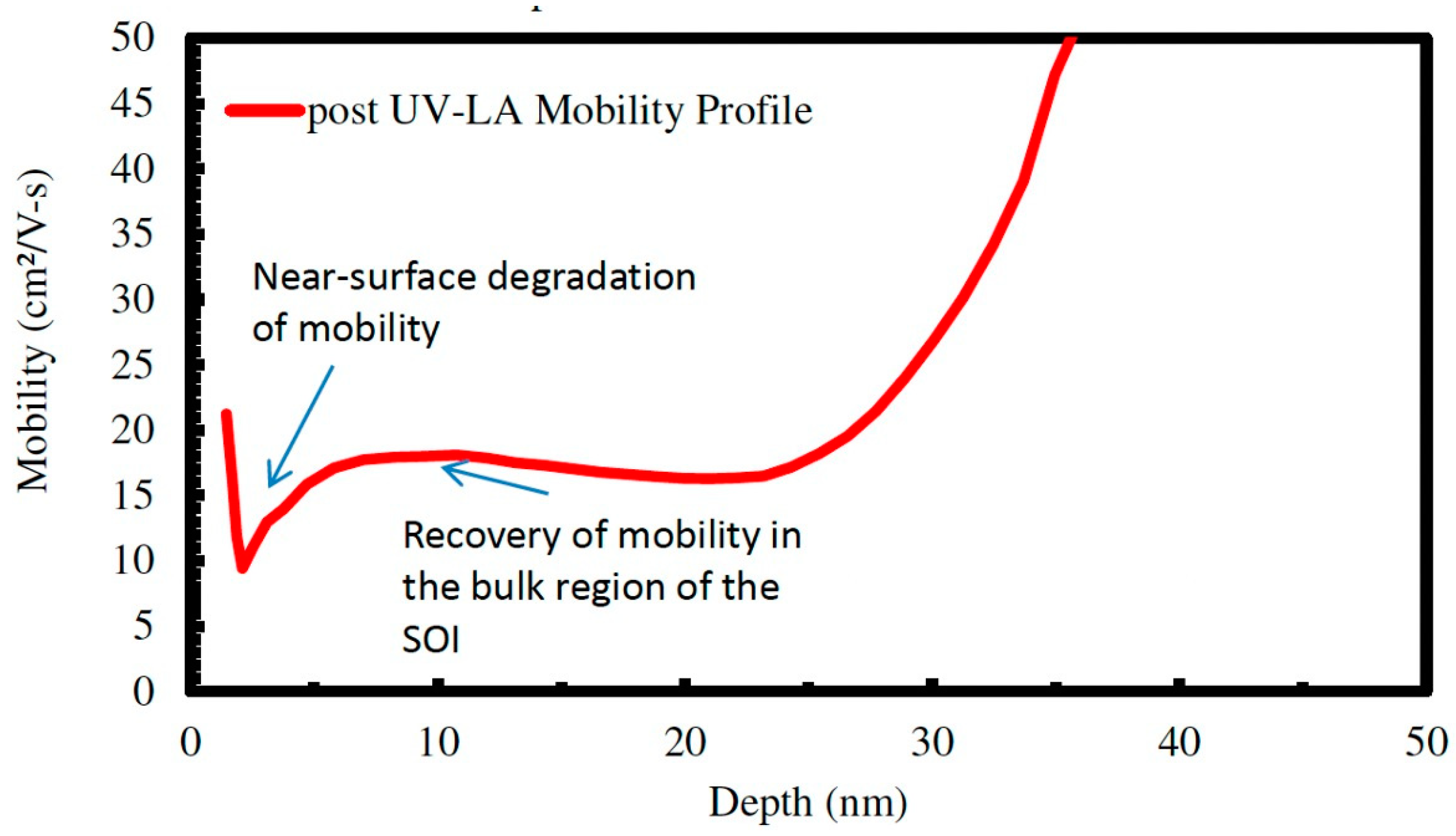
In another publication, physical and chemical data sets (SIMS, cross-sectional TEM—XTEM, fast Fourier transform mapping—FFTM) were compared with the electrical data from DHEM [81]. Figure 6 shows the near-surface DHEM mobility profile after the As-implanted Si sample was subjected to UV-LA. The near-surface mobility value in these data drops to ~50% of the bulk value. Models for As-doped Si do not predict such a large change in mobility, due to carrier scattering, for active dopant concentrations in the 1–3 × 1021 cm−3 range. Therefore, the reason for the reduction in mobility was assigned to defectivity. This result agreed well with the XTEM and FFTM data and demonstrated how DHEM can be used in a complementary fashion with other techniques, providing an electrical signature for observed defectivity.
Low contact resistance for Ge NMOS requires high dopant activation near the sample surface. Therefore, various approaches to improve doping for n-Ge are being developed. One such approach is co-doping. Figure 7 shows the SIMS, as well as the carrier concentration and resistivity depth profiles, taken from two samples, one a P-doped sample and the other a P + Sb-co-doped sample [82]. As can be seen from these data, the near-surface carrier concentration for the P-doped film is in the 1018 cm−3 range, whereas the co-doped film achieves a >1019 cm−3 active dopant density. Activation varies appreciably with depth, as demonstrated by DHEM. The effect of the cap layer employed during annealing was also evaluated in the same research. Comparing the SiO2 cap with the aluminum-oxide (Al-oxide) cap showed a drastic decline in the near-surface carrier density value for the sample with the Al-oxide cap. The reason was found to be carrier compensation by Al diffusion from the cap layer. DHEM was useful for identifying the exact location of the issue identified by bulk measurements.
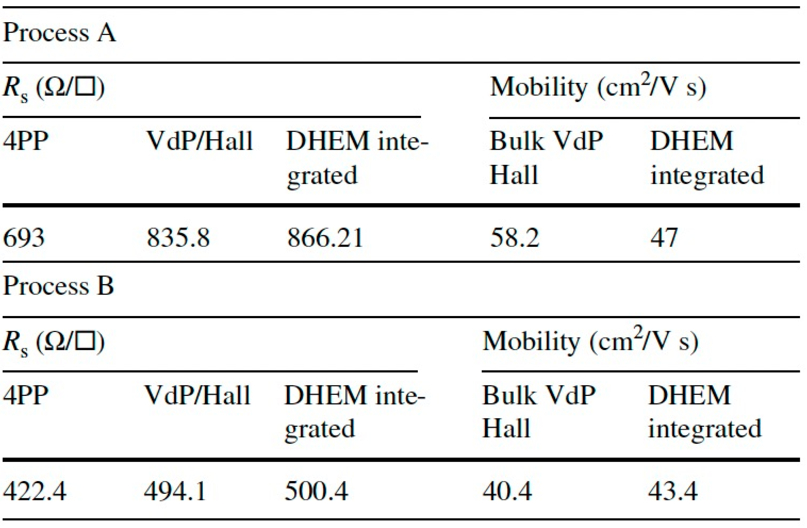
As the device size shrinks, the specific contact resistivity needs to be reduced to avoid deterioration of the device performance. Contact resistivity reduction requires high doping near the surface of the Si and SiGe films. Figure 8 and Figure 9 show the results of a study that was carried out to measure dopant activation in P-implanted Si films [79]. Si samples were doped under two different conditions (Process A and Process B). Process A included ion implantation of P followed by a millisecond anneal. Process B differed from Process A in that the ion implantation dose of P was tripled. As can be seen from Figure 9, the bulk electrical data obtained from 4PP and VdP/Hall effect measurements suggested that Process B might be more suitable for low resistivity ohmic contact formation since the sheet resistance was lower for this sample. However, the DHEM data of Figure 8 showed that dopant activation was, in fact, higher for Process A near the surface even though the implanted P amount was lower. Since the carrier concentration value near the surface is important for low resistivity contact formation, it was concluded that Process A would be more suitable for this application. If one relied solely on the bulk sheet resistance measurements to optimize the surface region dopant activation, one would be misled by those data. Figure 9 also provides the integrated Rs and mobility values calculated from the DHEM data. These values agree reasonably well with the bulk measurements.
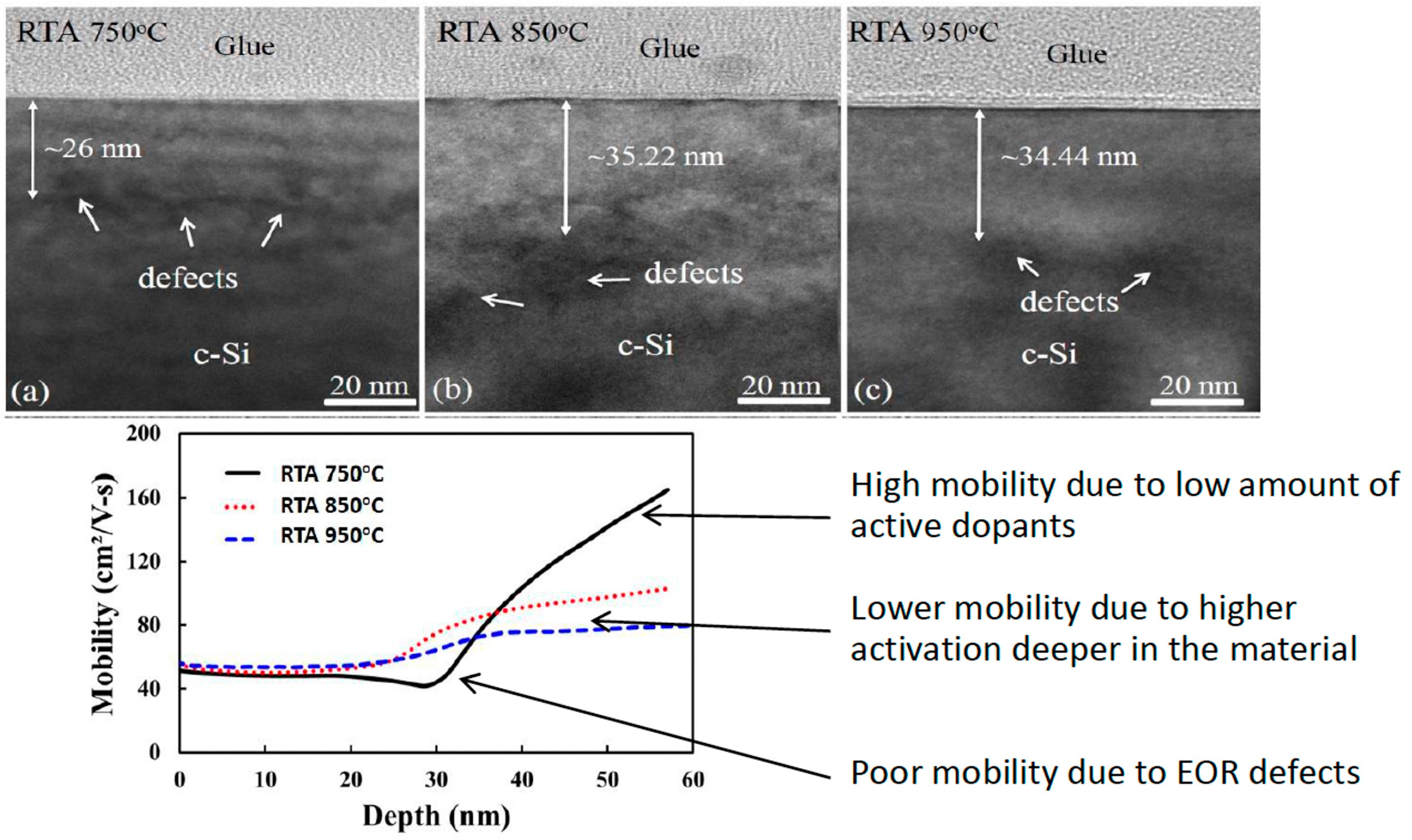
DHEM mobility depth profiles can be used to pinpoint the location of defectivity and optimize anneal regimes, as we have seen in the example of Figure 6. Yet another example of this application is shown in Figure 10, where TEM and DHEM results from P-implanted and annealed poly Si samples are presented [83]. Rapid thermal annealing (RTA) was performed at 750, 850 and 950 °C in this work. The TEM of the as-implanted sample showed a ~27 nm thick amorphized surface layer. The TEM data taken after annealing (Figure 10) indicated a gradual decrease in the end of range (EOR) defects with an increasing anneal temperature. The electrical signature of this phenomenon is clear from the DHEM mobility depth profile. The mobility for the sample treated at 750 °C dips at around the 25–30 nm range and then rises as measurements move into the low-doped crystalline region. With 850 and 950 °C heat treatments, one can observe that the mobility recovery rate at the EOR location is in good agreement with the TEM data, which show defects dissolving. The mobility value decreases in the crystalline region as the annealing temperature increases because of the diffusion of dopants deeper into the material.
A recent publication investigated the within grain and grain boundary dopant activation in P-implanted polycrystalline Si samples through complementary use of atom probe tomography (APT) and DHEM [84]. They found that post annealing dopant activations at the grain boundaries of the regrown and non-regrown regions of the material were 6% and 1%, respectively. In contrast, the within grain activations for the two regions were found to be 39% and 100%. This work highlighted a novel approach for evaluating site-specific activation ratios for poly Si through integrated use of DHEM and APT.
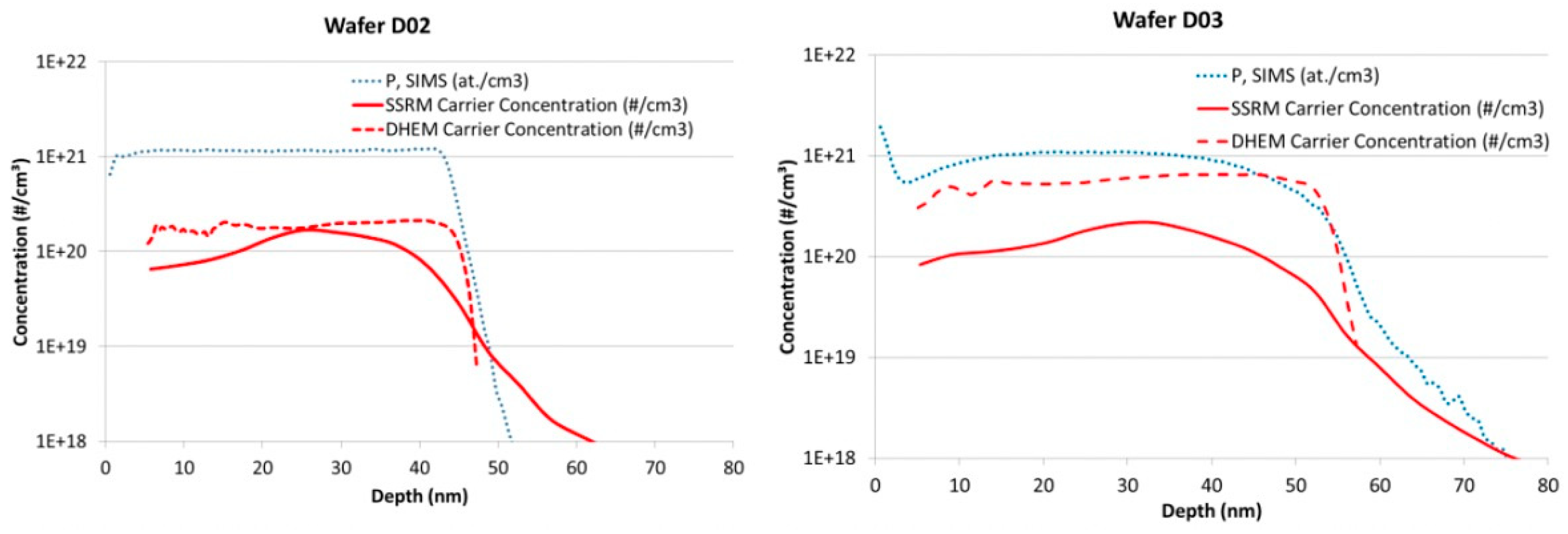
There has been literature comparing DHEM data with other depth profiling approaches. Celano et al. characterized dopant activation in heavily P-doped epi-Si layers as a function of certain process variables [76]. For electrical measurements, depth profiles of carrier concentration values were obtained using SSRM and DHEM. Figure 11 shows two of these profiles along with the SIMS data. The total dopant concentration, as measured by SIMS, showed a small difference between the as-deposited and spike-annealed samples. However, the spike-annealed sample indicated a much higher dopant activation, as measured by DHEM. The activation levels measured by SSRM, however, were lower for both samples, and the tail of the SSRM data was more graded. Bulk sheet resistance measured by DHEM agreed well with the 4PP data, and it was 138 and 64 Ω/square for samples D02 and D03, respectively. If the carrier levels were similar for the two samples (as suggested by SSRM), the larger thickness of sample D03 would reduce the sheet resistance value by about 20%. However, the reduction measured by 4PP was more than 100%. All the other comparisons with bulk measurements validated the dependability of the DHEM data. It should be noted that a few data points in the DHEM profile that went over the SIMS profile at around 55 nm (which is not possible) are still within the 10% error margin of the two techniques.
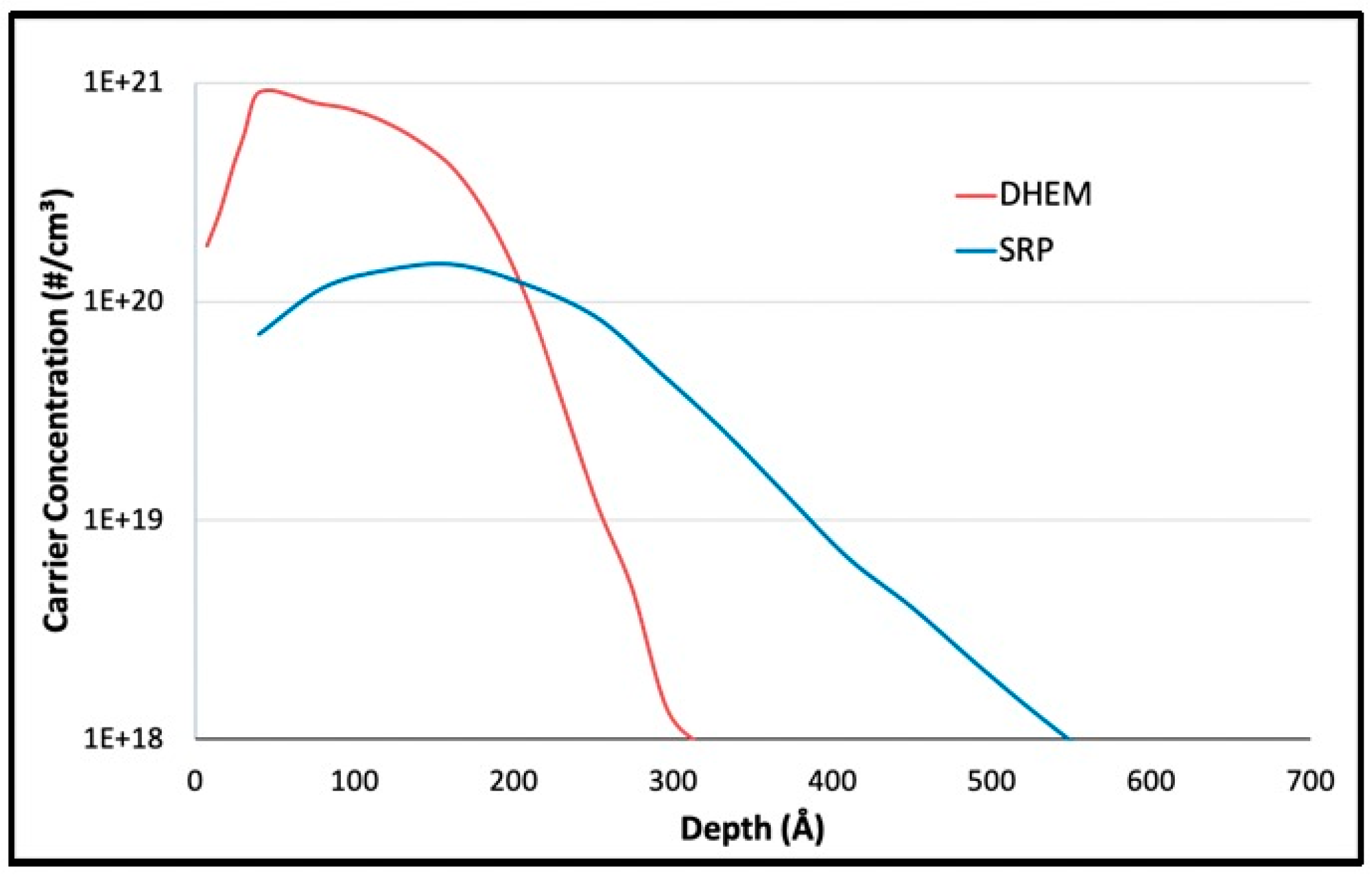
A similar work comparing SRP data with DHEM results was reported by Lin et al. [85]. SRP is known to be an effective technique for characterization of relatively deep junctions. However, it is expected to present limitations as the junctions become shallower. Lin et al. obtained the carrier concentration depth profiles from B- and As-implanted and annealed samples using SRP and DHEM. Figure 12 shows the data collected from the As-doped film.
As can be seen from these data, the junction is about 25 nm deep and there is a large discrepancy between the DHEM and SRP results. The bulk sheet resistance value measured by VdP for this sample was 198.4 Ω/square. Integrating the DHEM data through film thickness yielded a sheet resistance value of 207.9 Ω/square, which is reasonably close to the bulk value. In contrast, using the SRP depth profile, a value of 355.2 Ω/square was calculated, which was clearly in error. The B-doped sample that was characterized showed a similar behavior. It was concluded that SRP measurements of carrier concentration depth profiles underestimated the near-surface dopant activation. This finding is similar to the comparison of SSRM and DHEM [76], and it results from the fact that SRP and SSRM do not directly measure mobility. Using overestimated mobility values, especially near the surface, where factors such as defectivity and very high dopant concentration play an important role, result in the calculation of underestimated carrier concentrations.
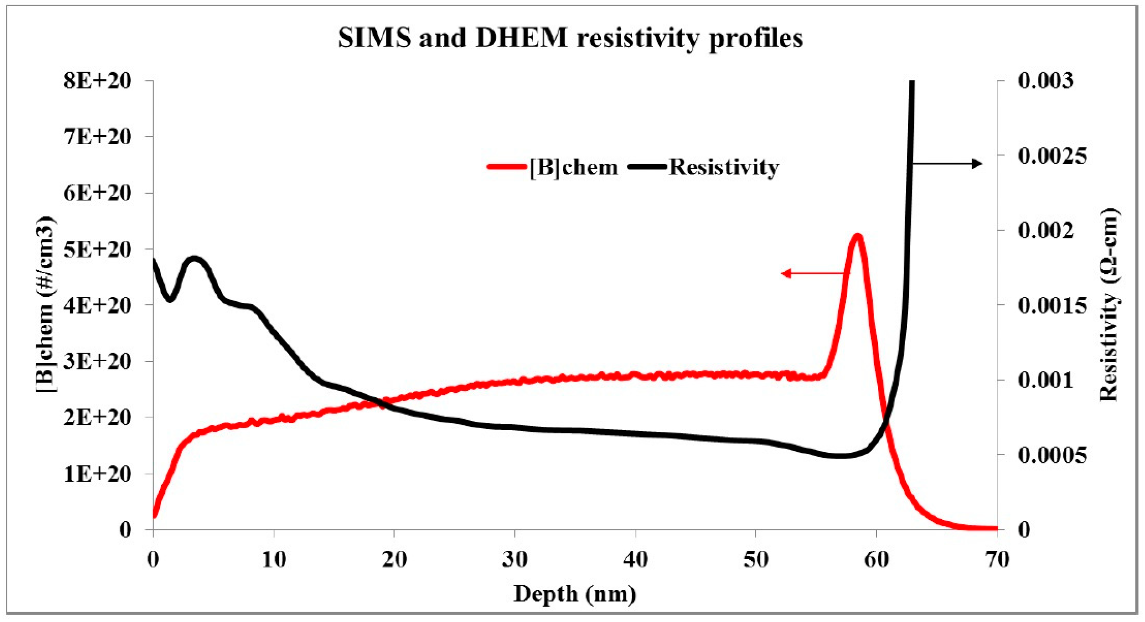
As stated before, DHEM can also characterize SiGe layers. Joshi et al. recently reported some results on B-doped Si0.5Ge0.5 epi layers grown on an n-type Si substrate [86]. Figure 13 compares the B chemical concentration profile with the layer resistivity profile measured by DHEM for that layer. As can be seen, resistivity is not constant throughout. It starts low, near the Si interface, where there is also a B pileup. Resistivity then increases as the B concentration declines towards the surface. It has been reported that B inclusion decreases as strain relaxation occurs; in this case, near the surface when the film becomes thick [87]. While the SIMS profile of Figure 11 provides that chemical signature, DHEM clearly shows the electrical consequence of this phenomenon. This could not be observed from just the bulk measurements.

6. Discussion of Assumptions and Uncertainties

As described above, DHEM involves thinning down the material under study in a stepwise manner and carrying out Hall effect/van der Pauw measurements after each thinning step. Thinning is achieved through electrochemical etching or oxide formation. Therefore, uncertainties need to be discussed for the material-thinning step as well as the electrical measurement steps.
For Si, experimental results showed that the oxide thickness control achieved through the control of the oxidation potential yields an overall depth scale accuracy within 10% of the value measured by SIMS. This is valid for constant experimental conditions, including a fixed electrolyte composition and electrochemical cell geometry. If these conditions are changed for any reason, a new calibration needs to be performed to relate the oxide thickness to the oxidation potential. During this calibration procedure, the oxide thickness can be measured by TEM. The 10% uncertainty in the Δz value reflects directly into the uncertainty in the calculated carrier concentration value, as can be seen in Equation (6).
DHEM utilizes a cross shaped test pattern for the Hall effect/van der Pauw measurements. Among the possible van der Pauw patterns (such as circular, square, clover leaf), the cross shape offers the lowest theoretically calculated error rate of <1% for ideal samples [88,89]. Ideal samples must have an absolutely uniform thickness in the test region, perfectly ohmic contacts, and a uniform material composition. In practice, however, it is almost impossible to meet all these conditions, and therefore error rates increase. For DHEM, the most important source of error in electrical measurements originate from the insulating interface (see Figure 2 and Figure 3). If the structure to be evaluated was an silicon-on-insulator (SOI), there would be no issue. If, however, electrical isolation is provided by a pn junction, the quality of the results would depend on the robustness of that junction. A leaky pn junction would allow some of the test current to pass into the substrate below, which interferes with the electrical measurements. This becomes more important as the film thickness is reduced and the test voltage needs to be boosted. Excessive contact probe penetration into the film also increases the risk of leakage through the pn interface for ultra-shallow junction measurements. Another factor contributing to larger electrical measurement errors is non-linear contacts, especially for higher-resistivity films. ALProTM tools implementing the DHEM technique make multiple (typically 5–20) Hall effect/van der Pauw measurements after each material removal step and calculate the standard deviation. A standard deviation of >10% often indicates an issue with the sample, as described above.
DHEM measurements are typically carried out on samples with native oxide. Since the thickness of this oxide layer may be in the range of 1–3 nm, electrical data cannot be collected for that region. This shows up clearly in the anodization voltage–current waveforms, where there would be a voltage but minimal or no current. This fact needs to be taken into account in comparing the SIMS profiles, which may include data from the surface oxide, with DHEM profiles, which start after the native oxide region.

7. Conclusions

Electrical property depth profiling through semiconductor films offers valuable information about the site-specific electronic properties of the material. Techniques such as SRP, SSRM and E-CV provide depth profiles for resistivity or carrier concentration. DHE techniques are unique in that they also measure mobility as a function of depth. The most advanced DHE approach is DHEM, which packages all capabilities of the technique in an automated tool. DHEM has a sub-nm depth resolution and a reasonably high throughput. Its applications include characterization of super-doped Si and SiGe ultra-shallow junctions fabricated using advanced deposition and annealing techniques, as well as measurement of dopant activation in Ge. Examples provided in this review demonstrate that complementary use of DHEM along with other characterization methods, such as SIMS, TEM, XTEM, FFTM, etc., provide valuable insight into the site-specific electrical quality of a film and correlate it with other factors such as chemical composition and defectivity. Although work so far has concentrated on the Group IV semiconductors, and, to a lesser extent, to GaAs, DHEM can be further developed to carry out measurements on a variety of other III-V compounds, conductive oxides such as indium gallium zinc oxide (IGZO), and important power electronics materials such as silicon carbide (SiC).

Author Contributions

Conceptualization, B.M.B. and A.J.; formal analysis, B.M.B. and A.J.; writing-original draft preparation, B.M.B.; writing-review and editing, A.J. All authors have read and agreed to the published version of the manuscript.

Funding

This work received no external funding.

Conflicts of Interest

The authors declare no conflict of interest.

References

  1. Mazur, R.G.; Dickey, D.H. A spreading resistance technique for resistivity measurements on silicon. J. Electrohem. Soc. 1966, 113, 255–259. [Google Scholar] [CrossRef]
  2. Vandervorst, W.; Clarysse, T.; Smith, H.E. Influence of the substrate doping level on spreading resistance profiling. J. Vac. Sci. Technol. B 1996, 14, 404–407. [Google Scholar] [CrossRef]
  3. Lin-Kwang, J.; Ramey, S.; Reynes, J.M.; Hillaed, R.J.; Thieme, T. The role of spreading resistance profiling in manufacturing control and technology development. Microelectron. Reliab. 2000, 40, 1497–1502. [Google Scholar] [CrossRef]
  4. Eyben, P.; Xu, M.; Duhayon, N.; Clarysse, T.; Callewaert, S.; Vandervorst, W. Scanning spreading resistance microscopy and spectroscopy for routine and quantitative two-dimensional carrier profiling. J. Vac. Sci. Technol. B 2002, 20, 471–478. [Google Scholar] [CrossRef]
  5. Clarysse, T.; Eyben, P.; Duhayon, N.; Xu, M.W.; Vandervorst, W. Carrier spilling revisited: On-bevel junction behavior of different electrical depth profiling techniques. J. Vac. Sci. Technol. B 2003, 21, 729–736. [Google Scholar] [CrossRef]
  6. Eyben, P.; Janssens, T.; Vandervorst, W. Scanning spreading resistance microscopy (SSRM) 2d carrier profiling for ultra-shallow junction characterization in deep-submicron technologies. Mater. Sci. Eng. B 2005, 124–125, 45–53. [Google Scholar] [CrossRef]
  7. Suchodolskis, A.; Hallen, A.; Gran, J.; Hansen, T.-E.; Karlsson, U.O. Scanning spreading resistance microscopy of shallow doping profiles in silicon. Nucl. Instrum. Methods Phys. Res. B 2006, 253, 141–144. [Google Scholar] [CrossRef]
  8. Dixon-Luinenburg, O.; Celano, U.; Vandervorst, W.; Paredis, K. Carrier profiling with fast Fourier transform scanning spreading resistance microscopy. A case study for Ge, GaAs, InGaAs, and InP. Ultramicroscopy 2019, 206, 112809. [Google Scholar] [CrossRef]
  9. Peiner, E.; Schlachetzki, A.; Kruger, D. Doping profile analysis in Si by electrochemical capacitance-voltage measurements. J. Electrochem. Soc. 1995, 142, 576–580. [Google Scholar] [CrossRef]
  10. Basaran, E.; Parry, C.P.; Kubiak, R.A.; Whall, T.E.; Parker, E.H.C. Electrochemical capacitance-voltage depth profiling of heavily boron-doped silicon. J. Cryst. Growth 1995, 157, 109–112. [Google Scholar] [CrossRef]
  11. Sermage, B.; Essa, Z.; Taleb, N.; Quillec, M.; Aubin, J.; Hartmann, J.M.; Veillerot, M. Electrochemical capacitance voltage measurements in highly doped silicon-germanium alloys. J. Appl. Phys. 2016, 119, 155703. [Google Scholar] [CrossRef]
  12. Essa, Z.; Taleb, N.; Sermage, B.; Broussillou, C.; Bazer-Bachi, B.; Quillec, M. Doping profile measurement on textured silicon surface. EPJ Photovolt. 2018, 9, 5. [Google Scholar] [CrossRef]
  13. Duhayon, N.; Clarysse, T.; Eyben, P.; Vandervorst, W.; Hellemans, L. Detailed study of scanning capacitance on cross-sectional and beveled junctions. J. Vac. Sci. Technol. B 2002, 20, 741–746. [Google Scholar] [CrossRef]
  14. Eyben, P.; Duhayon, N.; Alvarez, D.; Vandervorst, W. Assessing the resolution limits of scanning spreading resistance microscopy and scanning capacitance microscopy. AIP Conf. Proc. 2003, 683, 678–684. [Google Scholar] [CrossRef]
  15. Matey, J.R.; Blanc, J. Scanning capacitance microscopy. J. Appl. Phys. 1985, 57, 1437–1444. [Google Scholar] [CrossRef]
  16. Benstetter, G.; Biberger, R.; Liu, D. A review of advanced scanning probe microscope analysis of functional films and semiconductor devices. Thin Solid Films 2009, 517, 5100–5105. [Google Scholar] [CrossRef]
  17. Clarysse, T.; Vandervorst, W.; Lin, R.; Petersen, D.H.; Nielsen, P.F. Beyond SRP: Quantitative carrier profiling with M4PP. Nucl. Instrum. Methods Phys. Res. Beam Interact. Met. At. 2006, 253, 136–140. [Google Scholar] [CrossRef]
  18. Clarysse, T.; Eyben, P.; Parmentier, B.; Van Daele, B.; Satta, A.; Vandervorst, W.; Lin, R.; Petersen, D.H.; Nielsen, P.F. Advanced carrier depth profiling on Si and Ge with micro four-point probe. J. Vac. Sci. Technol. B 2008, 26, 317–321. [Google Scholar] [CrossRef]
  19. Clarysse, T.; Vanhaeren, D.; Vandervorst, W. Impact of probe penetration on the electrical characterization of sub-nm profiles. J. Vac. Sci. Technol. B 2002, 20, 459–466. [Google Scholar] [CrossRef]
  20. Eyben, P.; Duhayon, N.; Clarysse, T.; Vandervorst, W. Bias-induced junction displacements in scanning spreading resistance microscopy and scanning capacitance microscopy. J. Vac. Sci. Technol. B 2003, 21, 737–743. [Google Scholar] [CrossRef]
  21. Eyben, P.; Mody, J.; Vemula, S.; Vandervorst, W. Impact of environmental conditions on the electrical characteristics of scanning spreading resistance microscopy. J. Vac. Sci. Technol. B 2008, 26, 338–341. [Google Scholar] [CrossRef]
  22. Thurber, W.R.; Mattis, R.L.; Liu, Y.M.; Filliben, J.J. The Relationship between Resistivity and Dopant Density for Phosphorous and Boron Doped Silicon; National Bureau of Standards Special Publication 400-64; National Bureau of Standards: Washington, DC, USA, 1981. Available online: https://nvlpubs.nist.gov/nistpubs/Legacy/SP/nbsspecialpublication400-64.pdf (accessed on 14 August 2024).
  23. Cuttriss, D.B. Relation between surface concentration and average conductivity in diffused layers in germanium. Bell Syst. Tech. J. 1961, 40, 509–521. [Google Scholar] [CrossRef]
  24. Hall, E.H. On a new action of the magnet on electric currents. Am. J. Math. 1879, 2, 287–292. [Google Scholar] [CrossRef]
  25. Putley, E.H. The Hall Effect and Related Phenomena; Butterworths: London, UK, 1960. [Google Scholar]
  26. Van der Pauw, L.J. A method of measuring specific resistivity and Hall effect discs of arbitrary shape. Phil. Res. Rep. 1958, 13, 1–9. Available online: https://aki.issp.u-tokyo.ac.jp/okano/WalWiki/etc/VDP_PRR_13_1.pdf (accessed on 14 August 2024).
  27. Van der Pauw, L.J. A method of measuring the resistivity and Hall coefficient on lamellae of arbitrary shape. Phil. Tech. Rev. 1958, 20, 220–224. [Google Scholar]
  28. ASTM F76-08; Standard Test Methods for Measuring Resistivity and Hall Coefficient and Determining Hall Mobility in Single-Crystal Semiconductors. ASTM: West Conshohocken, PA, USA, 2016.
  29. Schroder, D.K. Mobility. In Semiconductor Material and Device Characterization, 3rd ed.; John Wiley & Sons: Hoboken, NJ, USA, 2006; pp. 465–475. [Google Scholar]
  30. Petritz, R.L. Theory of an experiment for measuring the mobility and density of carriers in the space-charge region of a semiconductor surface. Phys. Rev. 1958, 110, 1254–1262. [Google Scholar] [CrossRef]
  31. Tannenbaum, E. Detailed analysis of thin phosphorus-diffused layers in p-type silicon. Solid State Electron. 1961, 2, 123–132. [Google Scholar] [CrossRef]
  32. Iles, P.A.; Leibenhaut, B. Diffusant impurity concentration profiles in thin layers on silicon. Solid State Electron. 1962, 5, 331–339. [Google Scholar] [CrossRef]
  33. Nicholas, K.H. Studies of anomalous diffusion of impurities in silicon. Solid State Electron. 1966, 9, 35–47. [Google Scholar] [CrossRef]
  34. Tsai, J.C.C. Shallow phosphorus diffusion profiles in silicon. Proc. IEEE. 1969, 57, 1499–1506. [Google Scholar] [CrossRef]
  35. Whitton, J.L.; Carter, G.; Freeman, J.H.; Gard, G.A. The implantation profiles of 10, 20 and 40 keV 85Kr in gallium arsenide. J. Mater. Sci. 1969, 4, 208–217. [Google Scholar] [CrossRef]
  36. Davies, J.A.; Ball, G.C.; Brown, F.; Domeij, B. Range of energetic Xe125 ions in monocrystalline silicon. Can. J. Phys. 1964, 42, 1070–1080. [Google Scholar] [CrossRef]
  37. Subashchiev, V.K.; Poltinnikov, S.A. Determination of carrier mobility and density in the surface layer of a semiconductor. Sov. Phys. Solid State 1960, 2, 1059–1066. [Google Scholar]
  38. Buehler, M.G. A Point-Contact Method for Determining the Charge Carrier Density and Mobility in Thin Semiconducting Layers; Stanford Research Report. SEL-66-064; Stanford University: Palo Alto, CA, USA, 1966. [Google Scholar]
  39. Mayer, J.W.; Marsh, O.J.; Shifrin, G.A.; Baron, R. Ion implantation of silicon -electrical evaluation using Hall-effect measurements. Can. J. Phys. 1967, 45, 4073–4089. [Google Scholar] [CrossRef]
  40. Baron, R.; Shifrin, G.A.; Marsh, O.J.; Mayer, J.W. Electrical behavior of group III and V implanted dopants in silicon. J. Appl. Phys. 1969, 40, 3702–3719. [Google Scholar] [CrossRef]
  41. Johansson, N.G.E.; Mayer, J.W.; Marsh, O.J. Technique used in Hall effect analysis of ion implanted Si and Ge. Solid State Electron. 1970, 13, 317–335. [Google Scholar] [CrossRef]
  42. Cembali, F.; Galloni, R.; Mousty, F.; Rosa, R.; Zignani, F. Doping and radiation damage profiles of P+ ions implanted in silicon along the [110] axis. Radiat. Eff. 1974, 21, 255–264. [Google Scholar] [CrossRef]
  43. Hofker, W.K.; Werner, H.W.; Oosthoek, D.P.; Koeman, N.J. Boron implantations in silicon: A comparison of charge carrier and boron concentration profiles. Appl. Phys. 1974, 4, 125–133. [Google Scholar] [CrossRef]
  44. Kim, C.-S.; Sakata, M. Diffusion coefficient of selenium in silicon by sheet Hall coefficient measurements. Jpn. J. Appl. Phys. 1979, 18, 247–254. [Google Scholar] [CrossRef]
  45. Bennett, N.S.; Cowern, N.E.B. Doping characterization for germanium-based microelectronics and photovoltaics using differential Hall technique. Appl. Phys. Lett. 2012, 100, 172106. [Google Scholar] [CrossRef]
  46. Shin, B.K.; Look, D.C.; Park, Y.S.; Ehret, J.E. Hall-effect measurements in Cd-implanted GaAs. J. Appl. Phys. 1976, 47, 1574–1579. [Google Scholar] [CrossRef]
  47. McLevige, W.V.; Helix, M.J.; Vaidyanathan, K.V.; Streetman, B.G. Electrical profiling and optical activation studies of Be-implanted GaAs. J. Appl. Phys. 1977, 48, 3342–3346. [Google Scholar] [CrossRef]
  48. Whitehead, N.J.; Gwilliam, R.M.; Gillin, W.P.; Sealy, B.J. The use of Hall effect profiling to monitor the reactivation of silicon implants after oxygen implantation in gallium arsenide. Vacuum 1989, 39, 1149–1151. [Google Scholar] [CrossRef]
  49. Jackson, N.F. Pulsed anodic etching of III-V semiconductors for carrier concentration profiling. Semicond. Sci. Technol. 1992, 7, 686–690. [Google Scholar] [CrossRef]
  50. Clarysse, T.; Brammertz, G.; Vanhaeren, D.; Eyben, P.; Goossen, J.; Clemente, F.; Meuris, M.; Vandervorst, W.; Srnanek, R.; Kinder, R.; et al. Accurate carrier profiling of n-type GaAs junctions. Mater. Sci. Semicond. Process. 2008, 11, 259–266. [Google Scholar] [CrossRef]
  51. Plunkett, J.C.; Stone, J.L. A computer algorithm for accurate and repeatable profile analysis using anodization and stripping of silicon. Solid State Electron. 1977, 20, 447–453. [Google Scholar] [CrossRef]
  52. Hill, A.; Allen, W.G.; Bradley, R. An automatic smoothing algorithm for the calculation of impurity concentration from sheet resistivity and sheet Hall coefficient data. Solid State Electron. 1980, 23, 491–496. [Google Scholar] [CrossRef]
  53. Barber, H.D.; Lo, H.B.; Jones, J.E. Repeated removal of thin layers of silicon by anodic oxidation. J. Electrochem. Soc. 1976, 123, 1404–1409. [Google Scholar] [CrossRef]
  54. Galloni, R.; Gavina, G.; Lotti, R.; Piombini, A. An automated system for the controlled stripping of thin silicon layers. Rev. Phys. Appl. 1978, 13, 81–84. [Google Scholar] [CrossRef]
  55. Young, N.D.; Hight, M.J. Automated Hall effect profiler. Electron. Lett. 1985, 21, 1044–1045. [Google Scholar] [CrossRef]
  56. Blight, S.R.; Nicholls, R.E.; Sangha, S.P.S.; Kirby, P.B.; Teale, L.; Hiscock, S.P.; Stewart, C.P. Automated Hall profiling system for the characterization of semiconductors at room and liquid nitrogen temperatures. J. Phys. E Sci. Instrum. 1988, 21, 470–479. [Google Scholar] [CrossRef]
  57. Galloni, R.; Sardo, A. Fully automatic apparatus for the determination of doping profiles in Si by electrical measurements and anodic stripping. Rev. Sci. Instrum. 1983, 54, 369–373. [Google Scholar] [CrossRef]
  58. Bouro, L.; Tsoukalas, D. Determination of doping and mobility profiles by automatic electrical measurements and anodic stripping. J. Phys. E Sci. Instrum. 1987, 20, 541–544. [Google Scholar] [CrossRef]
  59. Alzanki, T.; Gwilliam, R.; Emerson, N.; Sealy, B.J. Differential Hall effect profiling of ultrashallow junctions in Sb implanted silicon. Appl. Phys. Lett. 2004, 85, 1979–1980. [Google Scholar] [CrossRef]
  60. Alzanki, T.; Gwilliam, R.; Emerson, N.; Sealy, B.J. Carrier and mobility profiling of ultra-shallow junctions in Sb implanted silicon. Electron. Lett. 2004, 40, 774–775. [Google Scholar] [CrossRef]
  61. Alzanki, T.; Gwilliam, R.; Emerson, N.; Smith, A.; Webb, R.; Sealy, B.J. Electrical profiles of 20nm junctions in Sb implanted silicon. Nucl. Instr. Meth. Phys. Res. B 2006, 242, 693–695. [Google Scholar] [CrossRef]
  62. Bennett, N.S.; Smith, A.J.; Colombeau, B.; Gwilliam, R.; Cowern, N.E.B.; Sealy, B.J. Differential Hall profiling of ultra-shallow junctions in Si and SOI. Mater. Sci. Eng. B 2005, 124–125, 305–309. [Google Scholar] [CrossRef]
  63. Bennett, N.S.; Cowern, N.E.B.; Smith, A.J.; Kah, M.; Gwilliam, R.M.; Sealy, B.J.; Noakes, T.C.Q.; Bailey, P.; Giubertoni, D.; Bersani, M. Differential Hall characterization of ultrashallow doping in advanced Si-based materials. Mater. Sci. Eng. B 2008, 154–155, 229–233. [Google Scholar] [CrossRef]
  64. Daubriac, R.; Abou Daher, M.; Cristano, F.; Scheid, E.; Joblot, S.; Barge, D. Differential Hall characterization of shallow strained SiGe layers. In Proceedings of the Nanotechnology Materials and Devices Conference, Toulouse, France, 9 October 2016. [Google Scholar] [CrossRef]
  65. Daubriac, R.; Scheid, E.; Rizk, H.; Monflier, R.; Joblot, S.; Beneyton, R.; Alba, P.; Kerdiles, S.; Cristano, F. A differential Hall effect measurement method with sub-nanometer resolution for active dopant concentration profiling in ultrathin doped SiGe and Si layers. Beilstein J. Nanotechnol. 2018, 9, 1926–1939. [Google Scholar] [CrossRef]
  66. Prussin, S.A. In Situ Determination of Resistivity, Mobility and Dopant Concentration Profiles. U.S. Patent 7,078,919, 18 July 2006. [Google Scholar]
  67. Prussin, S.A. The continuous anodic oxidation technique. AIP Conf. Proc. 2007, 931, 275–278. [Google Scholar] [CrossRef]
  68. Prussin, S.; Qin, S.; Reyes, J.; Mcteer, A. The application of the continuous anodic oxidation technique for evaluation of state-of-the-art frontend structures. AIP Conf. Proc. 2008, 1066, 75–78. [Google Scholar] [CrossRef]
  69. Timans, P.J.; Hu, Y.Z.; Lee, Y.; Gelpey, J.; McCoy, S.; Lerch, W.; Paul, S.; Bolze, D.; Kheyrandish, H.; Reyes, J.; et al. Optimization of diffusion, activation and damage annealing in millisecond annealing. In Proceedings of 16th IEEE International Conference on Advanced Thermal Processing of Semiconductors, Las Vegas, NV, USA, 30 September 2008. [Google Scholar] [CrossRef]
  70. Prussin, S.; Reyes, J. The evaluation of state-of-the-art front-end structures by differential Hall effect continuous anodic oxidation technique. ECS Trans. 2009, 19, 135–146. [Google Scholar] [CrossRef]
  71. Prussin, S.; Reyes, J. The application of differential Hall effect continuous anodic oxidation technique for ultra shallow structures. ECS Trans. 2009, 25, 139–150. [Google Scholar] [CrossRef]
  72. Qin, S.; Prussin, S.A.; Reyes, J.; Hu, Y.J.; McTeer, A. Study of low-energy doping processes using continuous anodic oxidation technique/differential Hall effect measurements. IEEE Trans. Plasma Sci. 2009, 37, 1754–1759. [Google Scholar] [CrossRef]
  73. Onoda, H.; Hamamoto, N.; Nagayama, T.; Sakai, S.; Tanjyo, M.; Umisedo, S.; Koga, Y.; Maehara, N.; Kawamura, Y.; Nakashima, Y.; et al. Effect of cluster carbon implantation at low temperature on damage recovery after rapid thermal annealing. In Proceedings of 18th IEEE International Conference on Advanced Thermal Processing of Semiconductors, Gainesville, FL, USA, 31 May 2010. [Google Scholar] [CrossRef]
  74. Qin, S.; McTeer, A.; Hu, Y.J.; Prussin, S.; Reyes, J. A comparative study of dopant activation and deactivation in arsenic and phosphorus implanted silicon. AIP Conf. Proc. 2011, 1321, 188–191. [Google Scholar] [CrossRef]
  75. Collart, E.J.H.; Kopalidis, P.M.; Hou, M.; McCoy, S.; Timans, P.J.; Joshi, A.; Prussin, S. Effects of implant temperature and millisecond annealing on dopant activation and diffusion. AIP Conf. Proc. 2012, 1496, 95–98. [Google Scholar] [CrossRef]
  76. Celano, U.; Wouters, L.; Franquet, A.; Spampinato, V.; van der Heide, P.; Schaekers, M.; Joshi, A.; Basol, B. Dopant activation depth profiling for highly doped Si:P by scanning spreading resistance microscopy (SSRM) and differential Hall effect metrology (DHEM). ECS Trans. 2022, 108, 9–15. [Google Scholar] [CrossRef]
  77. Joshi, A.; Basol, B. Sub-nm near-surface activation profiling for highly doped Si and Ge using differential Hall effect metrology (DHEM). ECS Trans. 2020, 98, 405–411. [Google Scholar] [CrossRef]
  78. Joshi, A.; Novak, S.W.; Basol, B.M. Differential Hall effect metrology (DHEM) for depth profiling of electrical properties at high resolution. In Proceedings of the International Conference on Frontiers of Characterization and Metrology for Nanoelectronics (FCMN), Monterey, CA, USA, 2 April 2019. [Google Scholar]
  79. Joshi, A.; Basol, B.M. Measuring activation depth profiles in very highly doped ultra-thin semiconductors at sub-nm depth resolution. MRS Adv. 2022, 7, 1326–1330. [Google Scholar] [CrossRef]
  80. Tabata, T.; Roze, F.; Thuries, L.; Halty, S.; Raynal, P.E.; Huet, K.; Mazzamuto, F.; Joshi, A.; Basol, B.M.; Alba, P.A.; et al. Microsecond non-melt UV laser annealing for future 3D-stacked CMOS. Appl. Phys. Express 2022, 15, 061002. [Google Scholar] [CrossRef]
  81. Joshi, A.; Tabata, T.; Roze, F.; Basol, B.M. Study of dopant activation in laser annealed highly doped arsenic-implanted Si by differential Hall effect metrology (DHEM). ECS Trans. 2022, 109, 329–333. [Google Scholar] [CrossRef]
  82. Ramesh, P.; Saraswat, K.C.; Joshi, A.; Basol, B.M.; Wang, L.; Buyuklimanli, T. Differential Hall effect metrology (DHEM) sub-nm profiling and its application to dopant activation in n-type Ge. ECS Trans. 2020, 97, 75–80. [Google Scholar] [CrossRef]
  83. Chang, H.-Y.; Wu, Y.-C.S.; Chang, C.-H.; Lin, K.-L.; Joshi, A.; Basol, B.M. Nano-scale depth profiles of electrical properties of phosphorus doped silicon for ultra-shallow junction evaluation. IEEE Trans. Semicond. Manuf. 2021, 34, 357–364. [Google Scholar] [CrossRef]
  84. Lin, K.-L.; Lee, F.-Y.; Chen, Y.-M.; Tseng, Y.-J.; Yen, H.-W. Complementary use of atom probe tomography (APT) and differential Hall effect metrology (DHEM) for activation loss in phosphorus-implanted polycrystalline silicon. Scr. Mater. 2024, 241, 115877. [Google Scholar] [CrossRef]
  85. Lin, K.-L.; Chang, C.H.; Joshi, A.; Basol, B.M. Comparison of dopant activation in Si as characterized by spreading resistance profiling (SRP) and differential Hall effect metrology (DHEM). In Proceedings of the International Conference on Frontiers of Characterization and Metrology for Nanoelectronics (FCMN), Monterey, CA, USA, 20 June 2022; Available online: https://drive.google.com/file/d/1KbglbuyqX_FxgDdLEh-1SHNQJNwGruuB/view (accessed on 14 August 2024).
  86. Joshi, A.; Rengo, G.; Porret, C.; Lin, K.-L.; Chang, C.-H.; Basol, B.M. Characterization of doping and activation processes using differential Hall effect metrology. ECS Trans. 2021, 102, 113–116. [Google Scholar] [CrossRef]
  87. Rengo, G.; Porret, C.; Hikavyy, A.Y.; Rosseel, E.; Nakazaki, N.; Pourtois, G.; Vantomme, A.; Loo, R. Highly doped Si1-xGex epitaxy in view of S/D applications. ECS Trans. 2020, 98, 27–36. [Google Scholar] [CrossRef]
  88. David, J.M.; Beuhler, M.G. A numerical analysis of various cross sheet resistor test structures. Solid State Electron. 1977, 20, 539–543. [Google Scholar] [CrossRef]
  89. De Mey, G. Potential calculations in Hall plates. In Advances in Electronics and Electron Physics; Marton, L., Marton, C., Eds.; Academic: New York, NY, USA, 1983; Volume 61, pp. 1–61. [Google Scholar] [CrossRef]
Figure 1. Sketch demonstrating the Hall effect in a conductor/semiconductor slab.
Metrology 04 00034 g001
Figure 2. Test pattern used in DHEM. From reference [76]. © The Electrochemical Society. Reproduced by permission of IOP Publishing. All rights reserved.
Metrology 04 00034 g002
Figure 3. In DHEM, the electrically active thickness of the semiconductor layer at the test region is reduced either by electrochemical etching (left) or electrochemical oxide formation (right).
Metrology 04 00034 g003
Figure 4. TEM cross-sections of Sample #1 and Sample #2, anodized at 13 V and 195 V, respectively. From reference [79]. Reproduced with permission from SNCSC.
Metrology 04 00034 g004
Figure 5. SIMS depth profiles after As implantation (as-imp) and after laser annealing (UV-LA) under two different conditions (Process A (a) and Process B (b)). DHEM depth profiles were taken only after laser annealing processes. The initial amorphous/crystalline interface (a/c) position and the As solid solubility in Si at ~ 1000 °C are also indicated. From reference [80].
Metrology 04 00034 g005
Figure 6. DHEM mobility depth profile taken from an As-implanted and UV-LA-treated Si sample. From reference [81]. © The Electrochemical Society. Reproduced by permission of IOP Publishing. All rights reserved.
Metrology 04 00034 g006
Figure 7. SIMS and DHEM (ALProTM activation and resistivity) depth profiles taken from P-doped and (Sb+P)-doped Ge samples. The anneal step was carried out with an SiO2 cap. From reference [82]. © The Electrochemical Society. Reproduced by permission of IOP Publishing. All rights reserved.
Metrology 04 00034 g007
Figure 8. SIMS and DHEM carriers and mobility profiles for two P-implanted samples. From reference [79]. Reproduced with permission from SNCSC.
Metrology 04 00034 g008
Figure 9. Sheet resistance (Rs) and mobility bulk values measured by 4PP and VdP/Hall effect for samples subjected to Process A and Process B. From reference [79]. Reproduced with permission from SNCSC.
Metrology 04 00034 g009
Figure 10. TEM cross-sections micrographs and DHEM mobility depth profiles for P-implanted samples annealed at (a) 750 °C, (b) 850 °C and (c) 950 °C. From reference [83]. Reprinted with permission from IEEE Trans. Semiconductor Manufacturing.
Metrology 04 00034 g010
Figure 11. SIMS, SSRM and DHEM depth profiles for two P-doped epi-Si samples. Sample D02 was in as-deposited form. Sample D03 was subjected to a spike anneal. From reference [76]. © The Electrochemical Society. Reproduced by permission of IOP Publishing. All rights reserved.
Metrology 04 00034 g011
Figure 12. SRP and DHEM carrier concentration depth profiles taken from an As-implanted and laser-annealed Si sample. Reproduced from reference [85] with permission from the American Vacuum Society (AVS).
Metrology 04 00034 g012
Figure 13. SIMS dopant depth profile, [B]chem and DHEM resistivity depth profile taken from SiGe (50% Ge) epi layer on Si substrate. Reproduced from reference [86]. © The Electrochemical Society. Reproduced by permission of IOP Publishing. All rights reserved.
Metrology 04 00034 g013
Disclaimer/Publisher’s Note: The statements, opinions and data contained in all publications are solely those of the individual author(s) and contributor(s) and not of MDPI and/or the editor(s). MDPI and/or the editor(s) disclaim responsibility for any injury to people or property resulting from any ideas, methods, instructions or products referred to in the content.