Article

Reflection and Refraction of a Spin at the Edge of a Quasi-Two-Dimensional Semiconductor Layer (Quantum Well) and a Topological Insulator

1
Kent Place School, Summit, NJ 07901, USA
2
Department of Electrical and Computer Engineering, Virginia Commonwealth University, Richmond, VA 23284, USA
3
Department of Electrical Engineering and Computer Science, University of Cincinnati, Cincinnati, OH 45221, USA
*
Author to whom correspondence should be addressed.
Magnetism 2022, 2(2), 117-129; https://doi.org/10.3390/magnetism2020009
Submission received: 22 January 2022 / Revised: 16 February 2022 / Accepted: 18 March 2022 / Published: 18 April 2022

Abstract

:
We derive the reflection and refraction laws for an electron spin incident from a quasi-two-dimensional semiconductor region (with no spin–orbit interaction) on the metallic surface of a topological insulator (TI) when the two media are in contact edge to edge. For a given incident angle, there can generally be two different refraction angles for refraction into the two spin eigenstates in the TI surface, resulting in two different ‘spin refractive indices’ (birefringence) and the possibility of two different critical angles for total internal reflection. We derive expressions for the spin refractive indices and the critical angles, which depend on the incident electron’s energy for given effective masses in the two regions and a given potential discontinuity at the TI/semiconductor interface. For some incident electron energies, there is only one critical angle, in which case 100% spin polarized injection can occur into the TI surface from the semiconductor if the angle of incidence exceeds that critical angle. The amplitudes of reflection of the incident spin with and without spin flip at the interface, as well as the refraction (transmission) amplitudes into the two spin eigenstates in the TI, are derived as functions of the angle of incidence.

Graphical Abstract

1. Introduction

Topological insulators (TI) have exotic metallic states on their surfaces that exhibit intriguing properties, such as spin-momentum locking [1]. They have been used for spin pumping into ferromagnets and the generation of spin orbit torques [2], and may have other important applications as well [1]. A TI has a spin-polarized surface and hence can drive a spin current into a ferromagnet that it is in contact with, which can then switch the magnetization of the ferromagnet to orient along the spin polarization of the current [2,3]. If the magnetization of the ferromagnet is bistable, one can utilize this methodology to switch between the two states. This has applications in magnetic logic and memory [4]. In this paper, we study the converse problem of driving a spin current into a TI. For this purpose, we study the problem of the reflection and refraction of an electron spin at the interface of a quasi-two-dimensional semiconductor quantum well (with weak or no spin–orbit interaction) and the metallic surface of a TI when the two materials touch at their edges. We show that when the electron is incident on the interface at an angle greater than a critical value, it will lead to 100% spin-polarized injection of electrons into the TI under carefully tailored situations, because the electron will refract into only one of the two spin eigenstates and no refraction will occur into the other spin eigenstate. An arrangement for restricting the angle of incidence to a selected value was described in ref. [5] and is not repeated here for the sake of brevity. In this case, only one spin eigenstate in the TI will be populated and the corresponding spin current will be injected into a magnet that the TI may be in contact with. This will switch the magnet’s magnetization to a desired orientation.

2. Theory

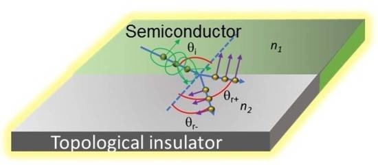
Consider the interface between a quasi-two-dimensional semiconductor and the surface of a TI, as shown in Figure 1, where region I is the semiconductor and region II is the TI. The edges of the two materials touch. Without loss of generality, we will consider that only the lowest subband is occupied by electrons in region I. We also ignore any spin–orbit interaction in region I. If region I is made of a wide bandgap semiconductor, then the Rashba spin–orbit interaction is weak [6] and the Dresselhaus spin–orbit interaction can also be weak, depending on the crystal structure. The semiconductor that we chose for our example later in Section 5 is CdTe (a wide band semiconductor) which has a relatively small Dresselhaus spin–orbit constant of 11.75 eV-Å3 [7]. Therefore, we can neglect spin–orbit interaction in the semiconductor.
The Hamiltonian for the composite system can be written approximately as [8,9]
H = p x 1 2 m ( x ) p x + p y 2 2 m ( x ) + V ( x ) + v 0 ( k x σ y k y σ x ) + λ 2 3 ( k + 3 + k 3 ) σ z ,
where, k ± = k x ± i k y , v0 is the Dirac cone velocity, σ-s are the Pauli spin matrices, λ is the band-structure warping constant and k+, k are wavevectors in the two spin eigenstates in the TI [8,9]. The quantities v0 and λ are zero in region I and non-zero in region II, while V(x) = V in region I and V(x) = 0 in region II.
Let us assume that, in region I, the effective mass of an electron is m I and, in region II, it is m II . Let us also call the wave vector components in region I ( k x , k y ) and in region II ( k x , k y ) . The energy dispersion relation of electrons in the surface of the TI (region II) can be obtained by diagonalizing the TI Hamiltonian, and can be written as [9,10].
E ± II = 2 ( k x 2 + k y 2 ) 2 m II ± 2 v k 2 ( k x 2 + k y 2 ) + 6 λ 2 ( k x 2 + k y 2 ) 3 cos 2 ( 3 ϕ ) 2 ( k x 2 + k y 2 ) 2 m II ± 2 v 0 2 ( k x 2 + k y 2 ) + 6 λ 2 ( k x 2 + k y 2 ) 3 cos 2 ( 3 ϕ )
where the two branches represent the dispersion relations in the two spin bands and ϕ is the azimuthal angle subtended by the electron wave vector with the x-axis. From Figure 1, it is obvious that ϕ is also the angle of refraction in region II. The energy dispersion relation in the quasi-2D semiconductor (region I), on the other hand, can be written as:
E I = 2 ( k x 2 + k y 2 ) 2 m I + V ,
where V is the (step) potential discontinuity at the interface.
The “spin refractive indices” ( n I , n II ) of the two regions for any incident electron energy will obey the relation [5]:
k I k II = k x 2 + k y 2 k x 2 + k y 2 = n I n II ,
where kI and kII are the magnitudes of the electron wave vectors for an arbitrary electron energy E in the two regions.
Using Equation (4), we will now define a quantity k as:
k = k x 2 + k y 2 n I = k x 2 + k y 2 n II .
The angles of incidence θi and refraction θr are defined in Figure 1. We note from this figure that k x = n I k cos θ i ,   k y = n I k sin θ i ,   k x = n II k cos θ r ,   k y = n II k sin θ r .
Since the Hamiltonian in Equation (1) is invariant in the y-coordinate, ky is a good quantum number. In other words, it is conserved across the interface, and hence k y = k y , which immediately yields the equivalent of Snell’s law from the last set of relations:
k y = k y sin θ i sin θ r = n II n I .
It is also easy to see from the conservation of the wave vector’s y-component that the angle of reflection is always equal to the angle of incidence in region I. This is, of course, identical to the situation in conventional optics.
We will now show that for any angle of incidence, there will be two different angles of refraction into the two spin eigenstates in the TI surface, and hence there will be two different refractive indices as well, as we had tacitly assumed. Since energy is conserved in the process of reflection/refraction (which are elastic events), we must have E I = E ± II = E , which yields from Equations (2) and (3):
2 ( k x 2 + k y 2 ) 2 m II ± 2 v 0 2 ( k x 2 + k y 2 ) + 6 λ 2 ( k x 2 + k y 2 ) 3 cos 2 ( 3 ϕ ) = 2 ( k x 2 + k y 2 ) 2 m I + V = E .
This equation immediately shows that there will be generally two different solutions for k x for the two spin eigenstates at any incident energy E and hence, according to Equation (4), there will be two different refractive indices n II ± for refracting into the two spin eigenstates in region II. Snell’s law (Equation (6)) will then ensure that, for a fixed angle of incidence, there will be two different refraction angles θ r ± which will obey the relation
2 ( n II ± ) 2 k 2 2 m II ± 2 v 0 2 ( n II ± ) 2 k 2 + 6 λ 2 ( n II ± ) 6 k 6 cos 2 ( 3 θ r ± ) = 2 n I 2 k 2 2 m I + V .
The last equation is derived by using Equation (5) in (7) and can be recast (using Equation (6)) as:
2 k 2 2 m II sin 2 θ i sin 2 θ r ± ± 2 v 0 2 k 2 n I 2 sin 2 θ i sin 2 θ r ± + 6 λ 2 sin 6 θ i sin 6 θ r ± ( n I ) 4 k 6 cos 2 ( 3 θ r ± ) = 2 k 2 2 m I + V n I 2 1 + 2 m I V n I 2 2 k 2 = m I m II sin 2 θ i sin 2 θ r ± ± 4 m I 2 v 0 2 2 k 2 n I 2 sin 2 θ i sin 2 θ r ± + 4 m I 2 2 k 2 λ 2 sin 6 θ i sin 6 θ r ± ( n I ) 4 cos 2 ( 3 θ r ± )
Because there are two different refractive indices in region II, it is obvious that there can be none, one, or two different critical angles of incidence. If there are two, we can find them by setting θ r ± = π / 2 radians in Equation (9). This yields an equation for the critical angle associated with the first refracted beam (or first spin eigenstate in region II) as:
E E V = ( m I m II ) sin 2 θ c + + v 0 2 m I E V sin θ c + ,
where we made use of the relation E = 2 n I 2 k 2 2 m I + V .
Equation (10) is a quadratic equation that yields two solutions for the critical angle of incidence for a spin refracting into the first spin eigenstate:
θ c ( 1 ) = arcsin [ v 0 m I 2 ( E V ) + v 0 2 m I 2 ( E V ) + ( m II m I ) E E V ] θ c ( 2 ) = arcsin [ v 0 m I 2 ( E V ) v 0 2 m I 2 ( E V ) + ( m II m I ) E E V ]
The solution θ c ( 2 ) is negative and is hence an extraneous solution. Negative refraction is a well-known phenomenon in optics, but is not relevant here.
The critical angles of incidence for a spin refracting into the second spin eigenstate are found from the quadratic equation:
E E V = ( m I m II ) sin 2 θ c v 0 2 m I E V sin θ c ,
which again yields two solutions:
θ c ( 3 ) = arcsin [ v 0 m I 2 ( E V ) + v 0 2 m I 2 ( E V ) + ( m II m I ) E E V ] θ c ( 4 ) = arcsin [ v 0 m I 2 ( E V ) v 0 2 m I 2 ( E V ) + ( m II m I ) E E V ]
The solution θ c ( 4 ) is negative and hence extraneous.
In order to obtain simplified and tractable expressions for the two refraction angles for a given angle of incidence, we will next neglect the warping effects and set λ = 0. Band warping has a strong effect on such phenomena as circular dichroism [11], but not so much on spin properties that we study here. Then, from Equation (9), we obtain the following expressions for the two refraction angles as a function of the incident angle:
sin θ r ± = sin θ i m I v 0 n I k + ( m I v 0 n I k ) 2 + m II m I ( 1 + 2 m I V 2 n I 2 k 2 ) = sin θ i v 0 m I 2 ( E V ) + m I 2 ( E V ) v 0 2 + m II m I ( E E V ) n II ± n I = sin θ i sin θ r ± = m I 2 ( E V ) v 0 2 + m II m I ( E E V ) v 0 m I 2 ( E V )
It is easy to see from Equation (14) that:
sin θ r + sin θ r = 2 m I m II v 0 E m I ( E V ) 2 sin θ i ,
which tells us that θ r + θ r . This then also means that n II n II + and θ c ( 3 ) θ c ( 1 ) . From Equations (11), (13) and (14), we can also recover the familiar relations (familiar from optics) that sin θ c ( 1 ) = n II + / n I ;   sin θ c ( 3 ) = n II / n I .

3. Calculating the Refraction and Reflection Amplitudes

The wave function of an electron in region I (with arbitrary spin polarization) can be written as:
Ψ I ( x , z ) = ( a b ) e i ( k x x + k y y ) + r ( a b ) e i ( k x x k y y ) + r ( a b ) e i ( k x x k y y ) ,
where the first term on the right-hand side is the incident wave and the last two terms constitute the reflected wave, with r being the reflection amplitude into the incident spin eigenstate and r’ the reflection amplitude into the orthogonal spin eigenstate, i.e., reflection with a spin flip. Note that [ a a + b b = 0 ;   | a | 2 + | b | 2 = | a | 2 + | b | 2 = 1 ] , where the asterisk denotes a complex conjugate. There can be a spin-flip at the interface for the reflected electron in the semiconductor quantum well (region I), and hence we will have to consider that possibility here.
Neglecting warping effects, the Hamiltonian in region II (see Equation (1)) can be written as:
H II = 2 ( k x 2 + k y 2 ) 2 m II + v 0 ( k x σ y k y σ x ) = ( 2 ( k x 2 + k y 2 ) 2 m II 0 0 2 ( k x 2 + k y 2 ) 2 m II ) + ( 0 i v 0 k x i v 0 k x 0 ) ( 0 v 0 k y v 0 k y 0 )
Using the result k x = n II k cos θ r ,   k y = n II k sin θ r , we can find that the two eigenspinors of this Hamiltonian are:
Φ ± II = 1 2 ( 1 ± i e i θ r ± ) .
Because θ r + θ r , the two eigenspinors are not mutually orthogonal. They do not have to be since they are actually eigenspinors of two different Hamiltonians due to the fact that k x + k x . Note that the spin orientations in these two eigenstates are perpendicular to the directions of the corresponding refracted beams, which is characteristic of spin-momentum locking. To see this, note that the spin polarization components in the two beams are S x + = ( / 2 ) [ Φ + II ] [ σ x ] [ Φ + II ] = sin θ r + = k y / ( k x + ) 2 + k y 2 ,   S x = ( / 2 ) [ Φ II ] [ σ x ] [ Φ II ] = sin θ r = k y / ( k x ) 2 + k y 2 ,   S y + = ( / 2 ) [ Φ + II ] [ σ y ] [ Φ + II ] = cos θ r + = k x + / ( k x + ) 2 + k y 2 ,   S y = ( / 2 ) [ Φ + II ] [ σ y ] [ Φ + II ] = cos θ r = k x / ( k x ) 2 + k y 2 ,   S z + = S z = 0 . This immediately shows that in region II, S k II in either refracted beam. Note also that, as a consequence of birefringence, which makes θ r + θ r , the spins in the two beams are not mutually antiparallel, since S x + S x and S y + S y . This of course happens due to the fact that the two eigenspinors in Equation (18) are not orthogonal.
The wave function of the refracted electron can be written as:
Ψ II ( x , y ) = t + 1 2 ( 1 i e i θ r + ) e i ( k x + x + k y y ) + t 1 2 ( 1 i e i θ r ) e i ( k x x + k y y ) ,
where t + is the transmission amplitude into the first spin eigenstate and t_ is that into the second spin eigenstate in the refraction medium (TI). The x-components of the wave vectors in the two refracted beams are, of course, k x ± . For an electron of energy E = 2 n I 2 k 2 2 m I + V incident from region I at an angle θ i on the interface, and these wavevector components in region II (TI) are given by the relations:
k x + = n II + n I n I k 1 n I 2 ( n II + ) 2 sin 2 θ i = n II + n I 2 m I ( E V ) 1 n I 2 ( n II + ) 2 sin 2 θ i k x = n II n I n I k 1 n I 2 ( n II ) 2 sin 2 θ i = n II n I 2 m I ( E V ) 1 n I 2 ( n II ) 2 sin 2 θ i
and in region I (semiconductor), they are given by the relations:
k x = n I k 1 sin 2 θ i = 2 m I ( E V ) 1 sin 2 θ i k y = k y = n I k sin θ i = 2 m I ( E V ) sin θ i
Since sin θ c ( 1 ) = n II + / n I ;   sin θ c ( 3 ) = n II / n I , the wave vector k x + becomes imaginary when θ i > θ c ( 1 ) , while the wave vector k x becomes imaginary when θ i > θ c ( 3 ) indicating the well-known fact that the refracted wave will be evanescent when the angle of incidence exceeds the critical angle.
Enforcing the continuity of the wave function at the junction between the two regions (at x = 0), we get that:
t + 1 2 ( 1 i e i θ r + ) + t 1 2 ( 1 i e i θ r ) = ( 1 + r ) ( a b ) + r ( a b ) ,
which can be re-written as:
1 2 [ 1 1 i e i θ r + i e i θ r ] [ t + t ] [ a a b b ] [ r r ] = [ a b ] .
Enforcing current continuity across the interface, we get that at x = 0:
[ p x m II + v 0 σ y ] Ψ II ( x , y ) | x = 0 = p x m I Ψ I ( x , y ) | x = 0 ,  
which yields:
k x + m II 1 2 t + ( 1 i e i θ r + ) + k x m II 1 2 t ( 1 i e i θ r ) + i 2 v 0 t + ( i e i θ r + 1 ) + i 2 v 0 t ( i e i θ r 1 ) = [ 1 r ] k x m I ( a b ) r k x m I ( a b )
and that can be recast as:
[ α β χ δ ] [ t + t ] + ( k x / m 1 ) [ a a b b ] [ r r ] = ( k x / m 1 ) [ a b ] ,  
where:
α = 1 2 ( k x + / m II + v 0 e i θ r + ) ; β = 1 2 ( k x / m II v 0 e i θ r ) χ = i 2 ( k x + / m II e i θ r + + v 0 ) ; δ = i 2 ( k x / m II e i θ r + v 0 )
Defining new matrices as [ A ] = 1 2 [ 1 1 i e i θ r + i e i θ r ] ;   [ B ] = [ a a b b ] ;   [ C ] = [ a b ] and [ A ] = [ α β χ δ ] , we can re-write Equation (23) as:
[ A ] [ t + t ] [ B ] [ r r ] = [ C ] ,  
and Equation (26) as:
[ A ] [ t + t ] + k x m I [ B ] [ r r ] = k x m I [ C ] .
From Equation (28), we get:
[ r r ] = [ B ] 1 [ A ] [ t + t ] [ B ] 1 [ C ] = [ B ] [ A ] [ t + t ] [ B ] [ C ] = [ B ] [ A ] [ t + t ] [ 1 0 ] ,  
where the dagger denotes Hermitian conjugate. Note that the matrix [ B ] is unitary, and hence its inverse is its Hermitian conjugate matrix.
Substituting the last result in Equation (29), we get:
( [ A ] + ( k x / m I ) [ A ] ) [ t + t ] = 2 ( k x / m I ) [ C ] [ t + t ] = 2 ( k x / m I ) ( [ A ] + ( k x / m I ) [ A ] ) 1 [ C ] [ r r ] = 2 ( k x / m I ) [ B ] [ A ] ( [ A ] + ( k x / m I ) [ A ] ) 1 [ C ] [ 1 0 ]
Let us now define a new 2×2 matrix [ D ] = 2 ( k x / m I ) ( [ A ] + ( k x / m I ) [ A ] ) 1 = [ d 11 d 12 d 21 d 22 ] . Then, from Equation (31), we get the transmission amplitudes in the three different intervals [ 0 , θ c ( 1 ) ] ,   [ θ c ( 1 ) , θ c ( 3 ) ] ,   [ θ c ( 3 ) , π / 2 ] for a given incident angle θ i as
t + = { d 11 a + d 12 b 0 0 ( for   0 θ i < θ c ( 1 ) ) ( for   θ c ( 1 ) θ i < θ c ( 3 ) ) ( for   θ c ( 3 ) θ i π / 2 ) t = { d 21 a + d 22 b d 21 a + d 22 b 0 ( for   0 θ i < θ c ( 1 ) ) ( θ c ( 1 ) θ i < θ c ( 3 ) ) ( for   θ c ( 3 ) θ i π / 2 ) ;  
while the reflection amplitudes are found from Equation (31).

4. Conservation of Probability Current

If we pre-multiply Equation (24) with [ Ψ II ( x , y ) ] (where the dagger denotes the Hermitian conjugate) we get that at x = 0
[ Ψ I ( x , y ) ] [ p x m II + v 0 σ y ] Ψ II ( x , y ) | x = 0 = [ Ψ I ( x , y ) ] p x m I Ψ I ( x , y ) | x = 0 .
However, at x = 0, Ψ I ( x , y ) = Ψ II ( x , y ) because of the continuity of the wavefunction. Using this result in the left-hand side of Equation (33), we get that at x = 0
[ Ψ II ( x , y ) ] [ p x m II + v 0 σ y ] Ψ II ( x , y ) | x = 0 = [ Ψ I ( x , y ) ] p x m I Ψ I ( x , y ) | x = 0
Equating the real parts on both sides of the previous equation we get that, in the most general case, when the angle of incidence does not exceed either critical angle and both angles of refraction are real, the probability current continuity equation becomes:
k x + m II [ | t + | 2 + 1 2 Re ( t + t ) 1 2 Re ( t + t ) cos ( θ r + θ r ) + 1 2 Im ( t + t ) sin ( θ r + θ r ) ] + k x m II [ | t | 2 + 1 2 Re ( t t + ) 1 2 Re ( t t + ) cos ( θ r θ r + ) + 1 2 Im ( t t + ) sin ( θ r θ r + ) ] + ν 0 [ | t + | 2 cos θ r + | t | 2 cos θ r ] 1 2 ν 0 [ Re ( t t + ) ( cos θ r cos θ r + ) Im ( t t + ) ( sin θ r + sin θ r + ) ] + 1 2 ν 0 [ Re ( t + t ) ( cos θ r + cos θ r ) Im ( t + t ) ( sin θ r + + sin θ r ) ] = k x m I [ 1 | r | 2 | r | 2 ] .
When there is no birefringence so that t + = t = t / 2 ;   θ r + = θ r ;   k x + = k x = k x , the above equation reduces to the familiar current continuity equation:
( k x / m II k x / m I ) | t | 2 = 1 | r | 2 | r | 2 .

5. Numerical Examples

For numerical examples, we consider the semiconductor material to be CdTe and the topological insulator to be Bi2Te3. This means m I = 0.11 m 0 and m II = 0.32 m 0 , where m 0 is the free electron mass. The band alignment of this heterostructure is shown in Figure 2 [12]. This means that V = +1.12 eV. The conduction band offset at the interface causes a delta-function electric field which can give rise to a localized Rashba-type spin–orbit interaction at the interface which might cause a spin-flip at the interface as the electrons transmit into region II. We ignore that effect here.
We will assume that an electron is incident on the interface from region I (CdTe) with a kinetic energy EV of 0.05 eV. If this is the Fermi energy, then this corresponds to a Fermi wave vector of 3.8 × 10⁸ m−1 and hence an electron concentration of ~2.29 × 10¹⁶ m−2 in the CdTe layer. This means E = 1.12 + 0.05 = 1.17 eV in the TI. The Dirac cone velocity ν0 in Bi3Te2 is about 4 × 10⁵ m/s [13]. From Equation (14), we get that for this energy, n II + / n I = 7.3 and n II / n I = 9.3. Since both ratios are greater than unity, there are no real solutions for the critical angles θ c ( 1 ) and θ c ( 3 ) . In other words, an incident spin will transmit into the topological insulator, regardless of the angle of incidence.
In order to have the lower refractive index ratio n II + / n I   1 , which will permit a real solution for at least the critical angle θ c ( 1 ) , we will need the Fermi energy EV in CdTe to be so high that it will require an impractical carrier concentration. Hence, for this material system, there are no critical angles, i.e., all incident angles will transmit and there will be no total internal reflection.
In Figure 3, we plot the refraction angles θ r + and θ r as functions of the incident angle θ i of the electron in region I (CdTe) obtained from Equation (14). We have verified that the two refraction angles satisfy the relation in Equation (15). In Figure 4, we plot k x + and k x as functions of the incident angle θ i obtained from Equation (20). We then calculate the squared magnitudes of the transmission amplitudes into the two spin eigenstates in the TI as well as the squared magnitudes of the reflection amplitudes with and without spin flip, | t + | 2 ,   | t | 2 ,   | r | 2 , and | r | 2 , as functions of the incident angle of the electron in region I for two different spin polarizations: x-polarized spin [ a = 1 / 2 ,   b = 1 / 2 ,   a = 1 / 2 ,   b = 1 / 2 ] and z-polarized spin [ a = 1 ,   b = 0 ,   a = 0 ,   b = 1 ] . These results are obtained from Equations (26)–(32) and shown in Figure 5 and Figure 6.
We call these quantities “squared magnitudes of the amplitudes”, instead of transmission and reflection “probabilities” for a reason. A probability cannot exceed unity, but the squared magnitudes can, as is obvious from Equation (36). This is the reason why in quantum transport literature the transmission probability is usually defined as ( k x / m II k x / m I ) | t | 2 instead of as | t | 2 because the former quantity cannot exceed unity, but the latter can.
One interesting feature in Figure 6 is that | t + | 2 = | t | 2 and | r | 2 = | r | 2 for all incident angles for z-polarized spin, but not for x-polarized spin. This feature can be derived analytically from the results presented here.

6. Conclusions

In conclusion, we have derived the laws of reflection and refraction of a spin at the interface of a quasi-2D semiconductor region and a topological insulator, touching on their sides, neglecting band warping effects.
Note that the problem we explored in this paper is not a transport problem; rather, it is an “interface” problem. The sharp interface between the semiconductor and the TI is of zero physical extent, and hence no transport can occur through the interface. Only what happens at the interface matters. What happens to the spin before reaching the interface (i.e., whether it suffers scattering, etc.) and what happens to the spin after it passes through the interface, are of no consequence and do not affect the laws of reflection and refraction. In the case of optics or electromagnetics, the laws of reflection and refraction are determined by the continuity of the electric and magnetic field components at the interface only, and what scattering the electromagnetic wave or light wave experiences before reaching the interface or after passing through the interface, does not affect Snell’s law. The same is true here.

Author Contributions

Conceptualization, S.B.; methodology, S.B., M.C.; software, S.S.; validation, R.F., S.B.; investigation, S.S., R.F., M.C., S.B.; resources, S.S., S.B.; writing—original draft preparation, S.B.; writing—review and editing, M.C., S.B.; supervision, S.B.; project administration, S.B. All authors have read and agreed to the published version of the manuscript.

Funding

This research received no external funding.

Institutional Review Board Statement

Not applicable.

Informed Consent Statement

Not applicable.

Data Availability Statement

Not applicable.

Acknowledgments

Saraswati Shee acknowledges Ron Cozad for teaching her MATLAB and helping her with coding for this project.

Conflicts of Interest

The authors declare no conflict of interest.

References

  1. Moore, J.E. The birth of topological insulators. Nature 2010, 464, 194. [Google Scholar] [CrossRef] [PubMed]
  2. Mellnik, A.R.; Lee, J.S.; Richardella, A.; Grab, J.L.; Mintun, P.J.; Fischer, M.H.; Vaezi, A.; Manchon, A.; Kim, E.-A.; Samarth, N.; et al. Spin-transfer torque generated by a topological insulator. Nature 2014, 511, 449. [Google Scholar] [CrossRef]
  3. He, Q.L.; Hughes, T.L.; Armitgae, N.P.; Wang, K.L. Topolgical spintronics and magnetoelectronics. Nat. Mater. 2022, 21, 15–23. [Google Scholar] [CrossRef] [PubMed]
  4. Wu, H.; Chen, A.; Zhang, P.; He, H.; Nance, J.; Guo, C.; Sasaki, J.; Shirokura, T.; Hai, P.N.; Fang, B.; et al. Magnetic memory driven by topological insulators. Nat. Commun. 2021, 12, 6251. [Google Scholar] [CrossRef] [PubMed]
  5. Bandyopadhyay, S.; Cahay, M.; Ludwick, J. Reflection and refraction of an electron spin at the junction between two quasi-two-dimensional semiconductor regions with and without spin-orbit interaction. Phys. Scr. 2021, 96, 065806. [Google Scholar] [CrossRef]
  6. Bandyopadhyay, S.; Cahay, M. Introduction to Spintronics, 2nd ed.; CRC Press: Boca Raton, FL, USA, 2015. [Google Scholar]
  7. Petrović, M.D.; Vukmirović, N. Spin relaxation in CdTe quantum dots with a single Mn atom. Phys. Rev. B 2012, 85, 195311. [Google Scholar] [CrossRef] [Green Version]
  8. Fu, L. Hexagonal warping effects in the surface states of the topological insulator Bi2Te3. Phys. Rev. Lett. 2009, 103, 266801. [Google Scholar] [CrossRef] [PubMed] [Green Version]
  9. Siu, Z.B.; Tan, S.; Jalil, M.B.A. Effective Hamiltonian of surface states of topological insulator thin films with hexagonal warping. AIP Adv. 2016, 6, 055706. [Google Scholar] [CrossRef] [Green Version]
  10. Witting, I.T.; Chasapis, T.C.; Ricci, F.; Peters, M.; Heinz, N.A.; Hautier, G.; Snyder, G.J. The thermoelectric properties of Bismuth Telluride. Adv. Electron. Mater. 2019, 5, 1800904. [Google Scholar] [CrossRef]
  11. Jung, W.; Kim, Y.; Kim, B.; Koh, Y.; Kim, C.; Matsunami, M.; Kimura, S.-I.; Arita, M.; Shimada, K.; Han, J.H.; et al. Warping effects in the band and angular momentum structures of the topological insulator Bi2Te3. Phys. Rev. B 2011, 84, 245435. [Google Scholar] [CrossRef] [Green Version]
  12. Le, K.-K.; Myers, T.H. Band structure measurement and analysis of the Bi2Te3 and CdTe (111)B heterojunction. J. Vac. Sci. Technol. A 2015, 33, 031602. [Google Scholar] [CrossRef]
  13. Chen, Y.L.; Analytis, J.G.; Chu, J.H.; Liu, Z.K.; Mo, S.K.; Qi, X.L.; Zhang, H.J.; Lu, D.H.; Dai, X.; Fang, Z.; et al. Experimental realization of a three dimensional topological insulator Bi2Te3. Science 2009, 325, 178. [Google Scholar] [CrossRef] [PubMed] [Green Version]
Figure 1. (a) The interface between a quasi-two-dimensional semiconductor and the surface of a TI when the two materials are placed edge to edge. An electron with arbitrary spin polarization is incident from region I (semiconductor) onto region II (TI) with an angle of incidence θ i . The spin refracts into the TI with two different angles of refraction θ r ± for the two spin eigenstates in the TI. (b) Fabrication steps for the structure.
Magnetism 02 00009 g001
Figure 2. Band alignment in the CdTe/Bi2Te3 hetero-interface.
Magnetism 02 00009 g002
Figure 3. Plot of refraction angles (into the two spin eigenstates) as functions of the incident angle for an electron energy of 1.17 eV in the topological insulator.
Magnetism 02 00009 g003
Figure 4. The wavevector components perpendicular to the CdTe/Bi2Te3 interface for the two spin eigenstates and for incident electron energy of 1.17 eV in the topological insulator (0.05 eV in the semiconductor).
Magnetism 02 00009 g004
Figure 5. Transmission and reflection probabilities as functions of angle of incidence at the CdTe/Bi2Te3 interface for an incident x-polarized spin where a = 1 / 2 ,   b = 1 / 2 ,   a = 1 / 2 ,   b = 1 / 2 for incident electron energy of 1.17 eV in the topological insulator (0.05 eV in the semiconductor).
Magnetism 02 00009 g005
Figure 6. Transmission and reflection probabilities as functions of angle of incidence at the CdTe/Bi2Te3 interface for an incident z-polarized spin where a = 1 ,   b = 0 ,   a = 0 ,   b = 1 for incident electron energy of 1.17 eV in the topological insulator (0.05 eV in the semiconductor).
Magnetism 02 00009 g006
Publisher’s Note: MDPI stays neutral with regard to jurisdictional claims in published maps and institutional affiliations.

