1. Introduction
Spin ices are geometrically frustrated magnetic materials that have been increasingly studied due to their potential technological applications in the transport, processing and storage of information [
1]. Specifically, they have been pointed out as interesting materials for advances in the area of magnetricity [
2], which involves the transport of magnetic charges, just as electricity involves the transport of electrical charges through associated currents, but with much lower dissipation loss. Other interesting applications are in magnonics, a research field that studies the application and effect of spin wave propagation in nanomagnetic materials [
3], and neuromorphic computing systems [
4]. Those materials can be found in the form of rare-earth insulating oxides, such as the pyrochlores Dy
2Ti
2O
7 and Ho
2Sn
2O
7, being characterized by having a highly macroscopically degenerate ground state that follows Pauling’s ice rule [
5]. The presence of high-energy vertices in the crystal, violating the ice rule, means that they exhibit collective excitations behaving like magnetic monopoles connected by a non-energetic Dirac string [
2].
Advances in lithography techniques have allowed the nanofabrication of a two-dimensional system denominated artificial spin ice (ASI) [
6], a certain extension of the natural one, with advantages such as more applicability in devices, control and variability of the system geometry, facility to explore degenerate levels and possibility to evaluate topologies [
7]. One disadvantage of these artificial systems is the energetic string connecting opposite magnetic charges, which arises due to its planar geometric characteristics [
8]. In order to diminish its energy, planar rectangular lattices were proposed [
9] and, subsequently, experimental evidence of quasi-degeneracy [
10], thermodynamic phase transitions [
11] and coercivity decrease [
12] were demonstrated by our group in critical rectangular lattices. Recently, an interesting proposal investigated the degeneracy that could be recovered for square ASIs when the nanomagnets are connected at the vertex [
13].
Investigating the degeneracy of the ground state for artificial ASI materials is very important, as it would allow the emergence of magnetic monopole–antimonopole pairs that are weakly linked by a low-energy string, a characteristic needed for optimal technological application. For the case of unconnected nanomagnets in non-thermodynamic samples, our research group showed that when the ratio between the horizontal and vertical spacing of the rectangle formed by the nanomagnets is equal to
, the sample presents the degenerate ground state [
9,
10,
11,
12], which is excellent for potential applications involving the transport and storage of information with low energy dissipation, as mentioned previously. For connected nanomagnet samples, ground state degeneracy implies the appearance of magnetic domain walls, which play a role similar to that of emerging monopoles. This type of lattice offers advantages such as the possibility of carrying out transport measures and applications involving non-volatile memory, high energy efficiency in computing and high information storage capacity related to memristive effects [
14,
15].
Generally, ASIs are composed of permalloy nanomagnets with material usually deposited using physical vapour deposition techniques. Although this method allows the growth of thin and controlled thicknesses of materials, being very useful for ASI thermodynamic samples, which should be very thin (∼3 nm) as a way to achieve the superparamagnetic regime [
16], it is expensive and time consuming and can make the lift-off process very tough.
In this work, we also propose the nanofabrication of ASIs using electrodeposition, a low-cost technique that provides the rapid deposition of materials. It is effective, highly reproducible, easily installable in a clean-room environment and facilitates the lift-off process. The simplicity of this method is an attraction in micro- and nanofabrication, as the entire process is executed under ambient conditions. Obtaining nanostructures with low roughness, shaped and without pinholes is essential in the fabrication of ASI samples; however, it is a challenge when electrodeposition is used, due to the very small deposition areas. Another parameter that requires great control is the thickness, which must be around 20 to 30 nm for non-thermodynamic samples and to assure magnetic single domains in each island instead of magnetic topological state formation in thicker nanoislands [
17].
We are going to apply here a specific protocol to obtain good nanomagnet samples with permalloy grown by electrodeposition in order to investigate the proposed degeneracy in square arrays of connected nanomagnets through magnetoresistive measurements performed on samples with different lattice parameters. It will be carried out through a comparison of resistance values, coercive fields and magnetoresistive signals as functions of different lattice parameters. These measurements can indirectly indicate the desired degeneracy with the emergence of domain walls that behave like emerging monopoles, considering the low resistance and coercive field presented by the connected square sample. In unconnected arrays, these characteristics indicate a decrease in the energy of the string that connects emerging monopoles, as seen in [
12], marking the degeneracy of the ground state. By analogy, it may also be possible to associate these observations in connected lattices. For the purpose of better understanding the magnetization reversal processes recorded by the MR measurements, we are going to support our findings by performing micromagnetic simulations following the same experimental geometries and material parameters.
2. Materials and Methods
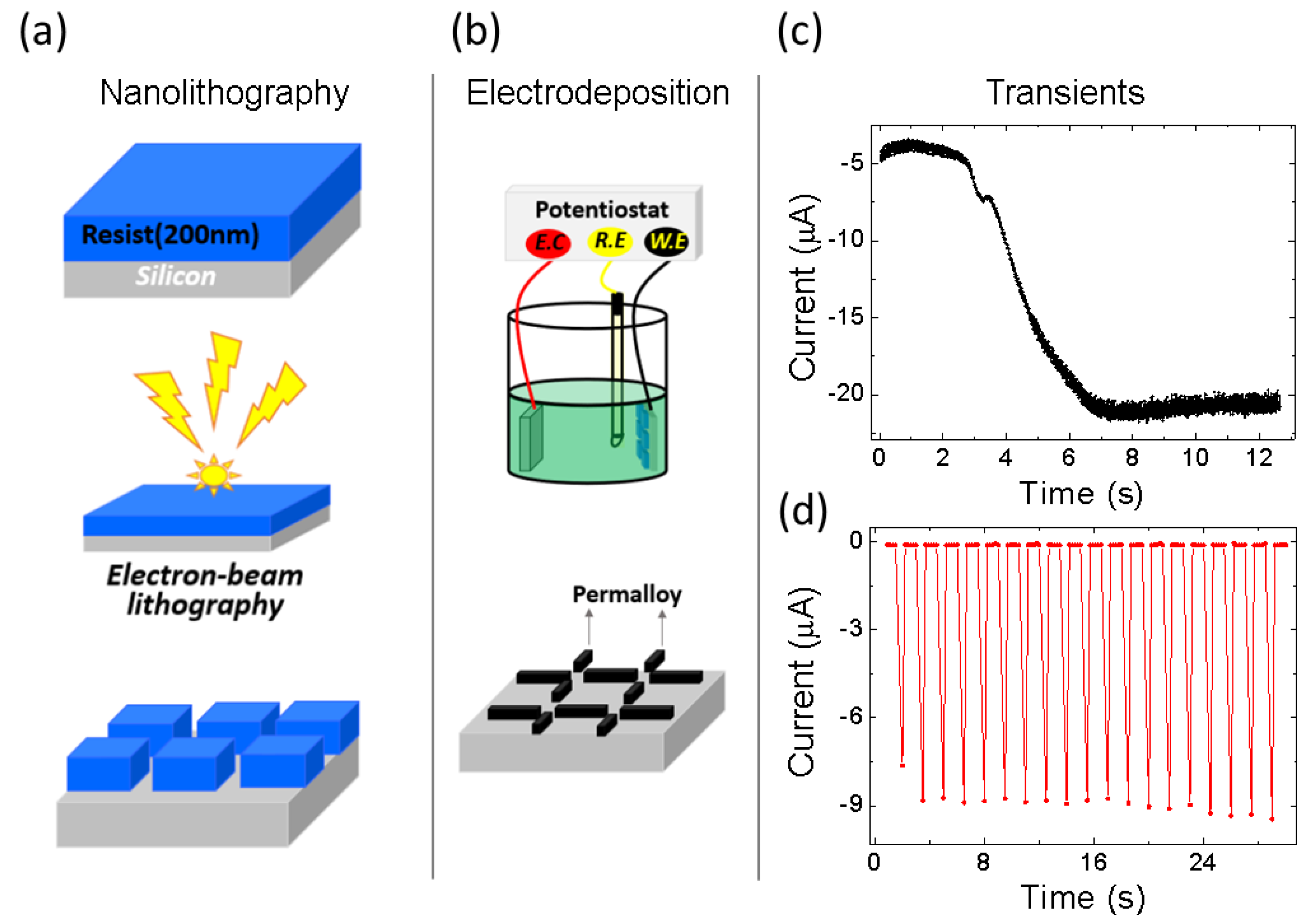
The ASI samples produced in this work were defined using electron-beam lithography (EBL) under 30 keV, executed using an scanning electron microscope with field emission source (FEG) model MIRA3 LMH TESCAN. This technique makes possible the definition of structures in the range of tens of nanometers with high resolution. The focused electron beam was used to establish a previous designed pattern relating to the sample shape delimitation on a substrate covered by a PMMA electroresist, which is chemically sensitive to this beam. A developing solvent was used to remove the regions of the positive electroresist exposed to the beam, as schematically described in
Figure 1a. After this nanolithography process conducted in a clean-room environment, electrodeposition of permalloy was performed over the entire substrate.
For the electrodeposition procedure, the n-type silicon (111) substrates with resistivity of 0.15
/cm
2, previously covered by the developed PMMA, were subjected to the standard cleaning procedure with acetone, isopropyl alcohol and 18M
deionized water. Subsequently, they were dipped in a 10% hydrofluoric acid solution to remove the native oxide layer inside the defined nanostructures. Thereafter, the samples were mounted on the working electrode of an electrochemical cell, as depicted in
Figure 1b, where permalloy was deposited using both constant and pulsed potentiostatic electrodeposition. Two protocols for the deposition were applied, electrodeposition performed by just inserting the samples in the electrolyte and after a previous sample dip for 10 s in 2% HF solution, in order to create an environment with greater wettability. The electrodeposition process occurred in an electrochemical cell containing the aqueous electrolyte based on references [
18,
19] and with lower concentrations of 30 mM FeSO
4, 30 mM NiSO
4, 2 mM NiCl
2, 20 mM saccharin and 40 mM H
3BO
3. A platinum counter electrode and Ag/AgCl type reference electrode were used to close the cell and the desired potentials were controlled by means of a commercial potentiostat.
Both constant and pulsed potentials of −1.1 V were used. The pulsed process consisted of applying a 0.5 s potential pulse, waiting 1s in the cell open regime and then applying the pulse again. This process guarantees, at the beginning, the formation of more nuclei per area, thus causing the film to be uniform with a lower thickness. Decreasing the concentration makes the process slower, consequently reducing the roughness. The deposits were obtained with 12 pulses, which guaranteed a thickness of approximately 30 nm. The samples were then again submitted to a nanolithography process in order to define the electrode geometries to enable MR measurements. For the copper electrode development, electrodeposition was also performed, this time using a solution composed of 0.6 M CuSO4 + 1.8 M C3H6O3 + 5 M NaOH with PH = 12 under a constant potential of −1 V.
During MR measurements, the samples were subjected to an external magnetic field generated by an electromagnet, applied perpendicularly to the direction of the constant electric current of 1 mA passing through the samples in the direction of the rectangles’ main axis.
Micromagnetic simulation in the rectangular connected lattices of size
m ×
m was performed with the open-source GPU-based software
[
20]. The permalloy numerical parameters used were magnetic saturation
A
, polarization
, exchange constant
J
and Gilbert damping α = 0.1. Periodic boundary conditions were used with finite difference discretization for the iterations based on the Landau–Lifshitz–Gilbert (LLG) equation (Equation (
1) with cubic cell of 5 nm × 5 nm × 5 nm).
The theoretical magnetoresistive signal obtained from the simulations was achieved by using the equation proposed for anisotropic magnetoresistance (AMR), taking into account a combination of current and magnetization according to [
15,
21]:
where
and
are the resistivity parallel and perpendicular to the normalized magnetization vector
, respectively, and
is the current density. We assume
. The physical origin of the effect is well-documented and is due to the scattering properties of electrons, depending on the orientation of magnetization [
22]. The first term in Equation (
2) is related to Ohm’s law in the continuous medium and the second one is the first-order contribution to the electric field due the AMR effect [
22].
3. Results and Discussion
There are several studies showing that potentiostatically electrodeposited permalloy of thicknesses on the order of a few tens of nanometers does not produce conformal films, only agglomerates [
18,
19]. Therefore, greater thicknesses would be needed to form uniform films and suitable ASI lattices. In contrast, in this work we show that by changing some concentration parameters in the electrolyte solution, performing a previous dip of the sample in a 2% HF aqueous solution and using pulsed potentiostatic electrodeposition, it is possible to produce lattices with the same quality as more sophisticated techniques, but with less cost and time. The deposition transients obtained in both processes are, respectively, presented in
Figure 1c,d.
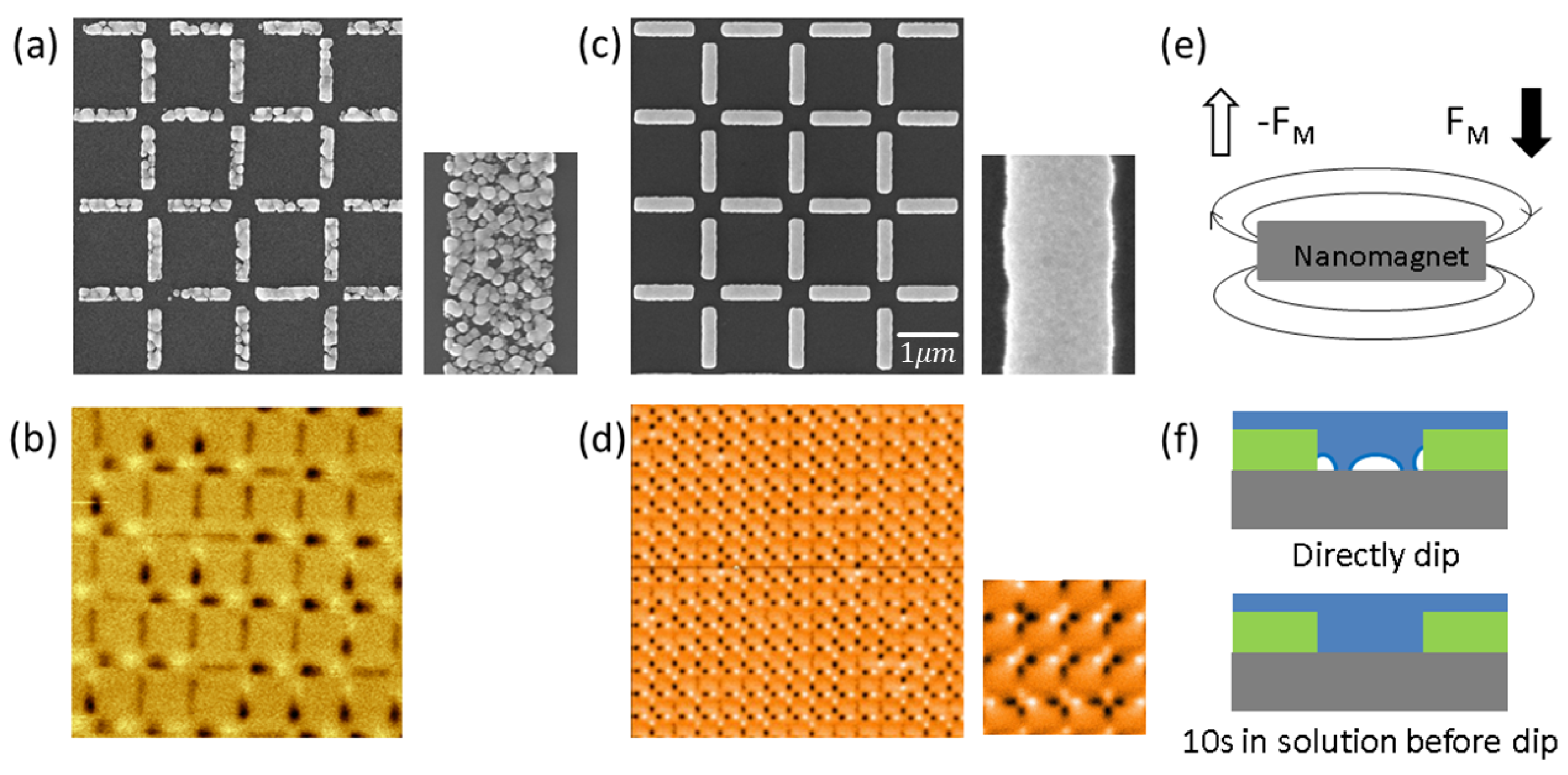
Considering the need to verify the effectiveness of the electrodeposition technique for ASI nanofabrication, characterizations were carried out by SEM and MFM, as shown in
Figure 2. In the SEM image in
Figure 2a, performed on the sample developed with constant potential deposition (transient presented in
Figure 1c), it is possible to see that the lattice geometry is not homogeneous and the films obtained in the nanomagnets (presented in the zoomed-in view) are presenting larger and non-uniform grains. Those characteristics prevent a good magnetic characterization of the nanomagnets and the ASI as a whole, as can be seen in
Figure 2b, showing some lack of dark and bright spots, which are related to the north and south directions of each nanomagnet. Probably it happens because the large grains allow non-uniformity in sample thickness and the formation of magnetic domains in plane, which are not sensed by the MFM tip, as indicated in the sketch in
Figure 2e.
Now, in
Figure 2c, we present the images taken of the sample developed with the improved pulsed electrodeposition protocol described above. Here, one can see that both the geometry and film uniformity were largely improved in an unconnected lattice of 100 μm × 100
m whose nanomagnet dimensions are 3 μm × 200 nm with a thickness of 30 nm. MFM measurements indicate the successful fabrication of ASI nanostructures using pulsed potentiostatic electrodeposition through the visualization of magnetic domains and the characteristic topologies between the vertices of the lattice formed by the nanomagnets, with all the sample nanomagnets presenting a large signal of bright and dark spots, characteristic of ASI systems. We attribute that success to the improvement in the sample’s wettability and formation of smaller permalloy grains due to the potentiostatic electrodeposition mode. Without such a process, air bubbles could be formed inside the nanostructures developed in the hydrophobic electroresist, as depicted in the sketch in
Figure 2f, preventing the total transference of the desired geometry.
In several ASI investigations found in the literature, the conventional square geometry is the most used due to its ground state obeying the ice rule. However, it is not possible to observe degenerate fundamental states at room temperature in square unconnected lattices, like in its natural counterpart, due to the consequent confinement of Nambu-like monopoles by an energetic string, as described above [
8]. As mentioned earlier in this article, recent studies performed by our group show that although degeneracy does not occur for this geometry, for rectangular unconnected ASI lattices (more specifically, when the ratio between the horizontal and vertical distances of the nanomagnets is equal to
), the degeneracy of vertices that obey the ice rule occurs [
9,
10,
11].
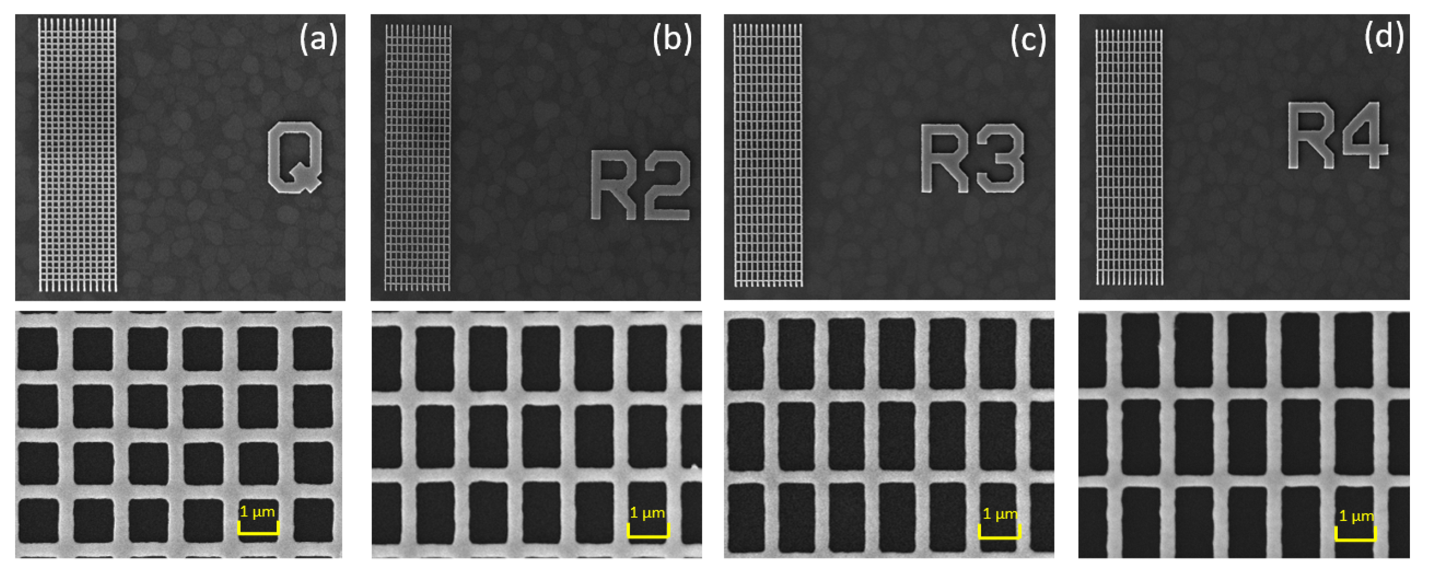
For the purpose of moving forward to electrical transport characterizations, different geometries of lattices containing connected nanomagnets were also successfully fabricated using the pulsed potentiostatic electrodeposition technique (
Figure 3). Here, the main goal is to apply characterizations by magnetoresistance (MR), considering the effectiveness of transport measures for potential applications of ASIs in devices, in addition to indirectly evaluating the degeneracy of the ground state for connected square geometry, as predicted in the literature [
13]. The samples were developed with dimensions of 18
m × 50
m and a thickness of 30 nm. Contact pads of copper were also developed by nanolithography and electrodeposition, but with a constant potential of −1 V in this case, once they could be thicker than the ASI geometries.
In that regard, we have investigated connected lattices with the ratio between the sides varying between 1, , and with the intention of evaluating how the coercivity changes between them and how this information can contribute to the indirect investigation of degeneracy in these systems, in comparison to previous investigations of string energy connecting emerging magnetic monopoles in regular unconnected lattices. Such knowledge could be very valuable and strictly related to the technological application of connected ASIs.
A recent study [
13] indicated that by connecting the vertices in square ASIs, the degeneracy of the ground state goes from rectangular, observed in the non-connected samples, to square. As in the degenerated state the quasi-vanishing of the energetic string will represent the low energy needed from the external magnetic field to extend it along the sample, one expects that the coercivity in degenerate systems would be lower than that in non-degenerate systems. In fact, this was already observed by us in unconnected ASI samples [
12,
23].
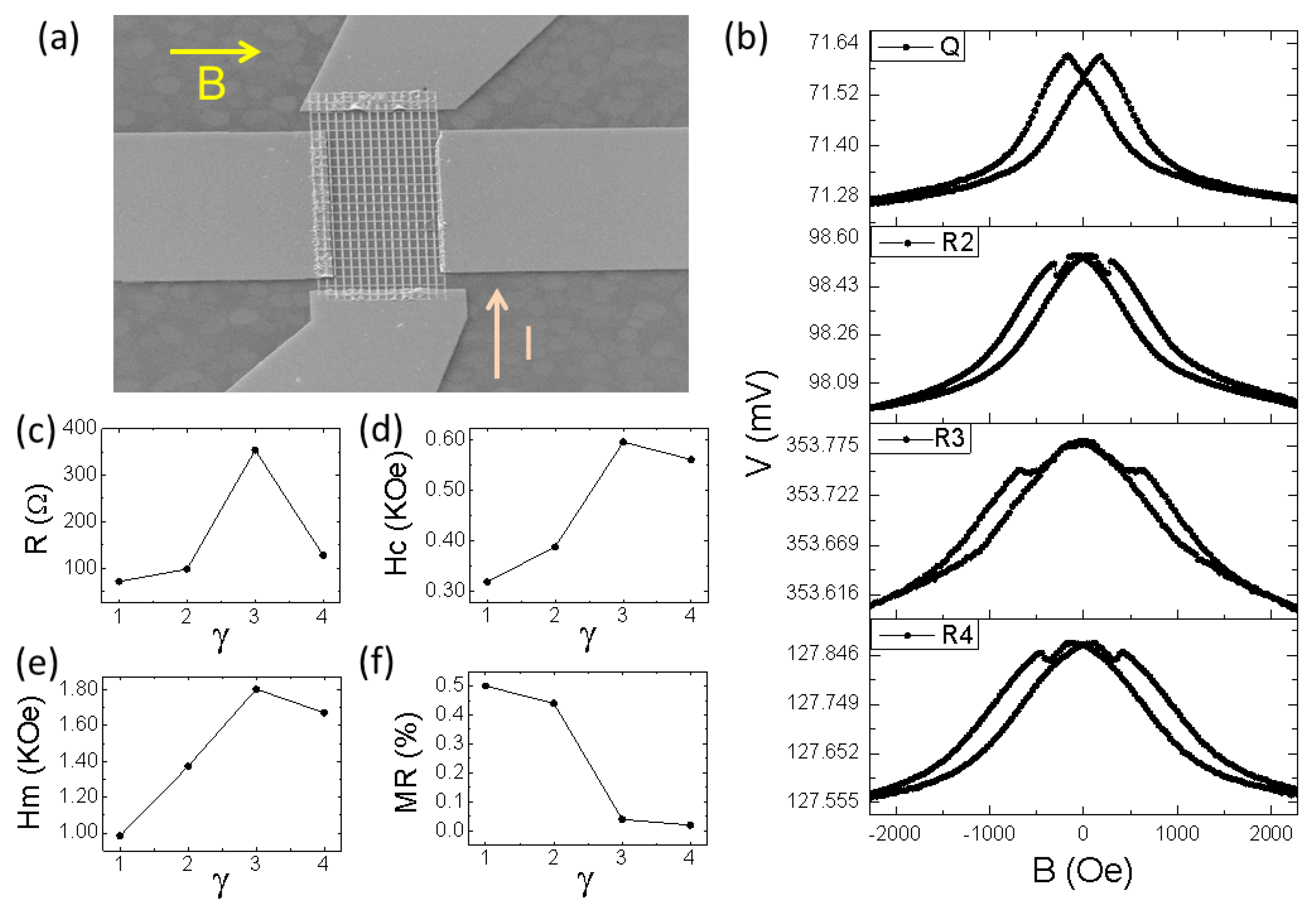
An example of the samples utilized here for the MR measurements is presented in
Figure 4a, indicating the direction of applied current throughout the large size of the lattice and the magnetic field aligned perpendicularly to the stripes. The magnetoresistive curves obtained with an applied current of 1mA are presented in
Figure 4b. Here, one can see that resistance is large at lower fields and decreases for higher fields in all samples. Such isotropic behavior is similar to that presented in magnetic multilayers with giant magnetoresistance [
24,
25]. In the present system, the main behavior characterized by two peaks pointing up arises due to the different magnetization of each nanowire branch, which represents resistive paths for the applied current. The smaller peaks pointing down are related to the anisotropic magnetoresistance due to the non-trivial magnetization on the vertex between nanowire branches. Such behavior was previously investigated in the literature [
15,
21].
In
Figure 4c–f, we summarize, respectively, the values of sample resistance, coercive field of smaller peaks, coercive field at half height of main peaks and magnetoresistive signals taken from the measurements presented in
Figure 4b. From these results, it is possible to conclude that the lowest energy expended to switch nanomagnet magnetization was found in the square geometry, corroborating the predicted quasi-degeneracy. Interestingly, the largest energy now expended by the field was found in the
geometry, the one presenting quasi-degeneracy in non-connected ASI geometries.
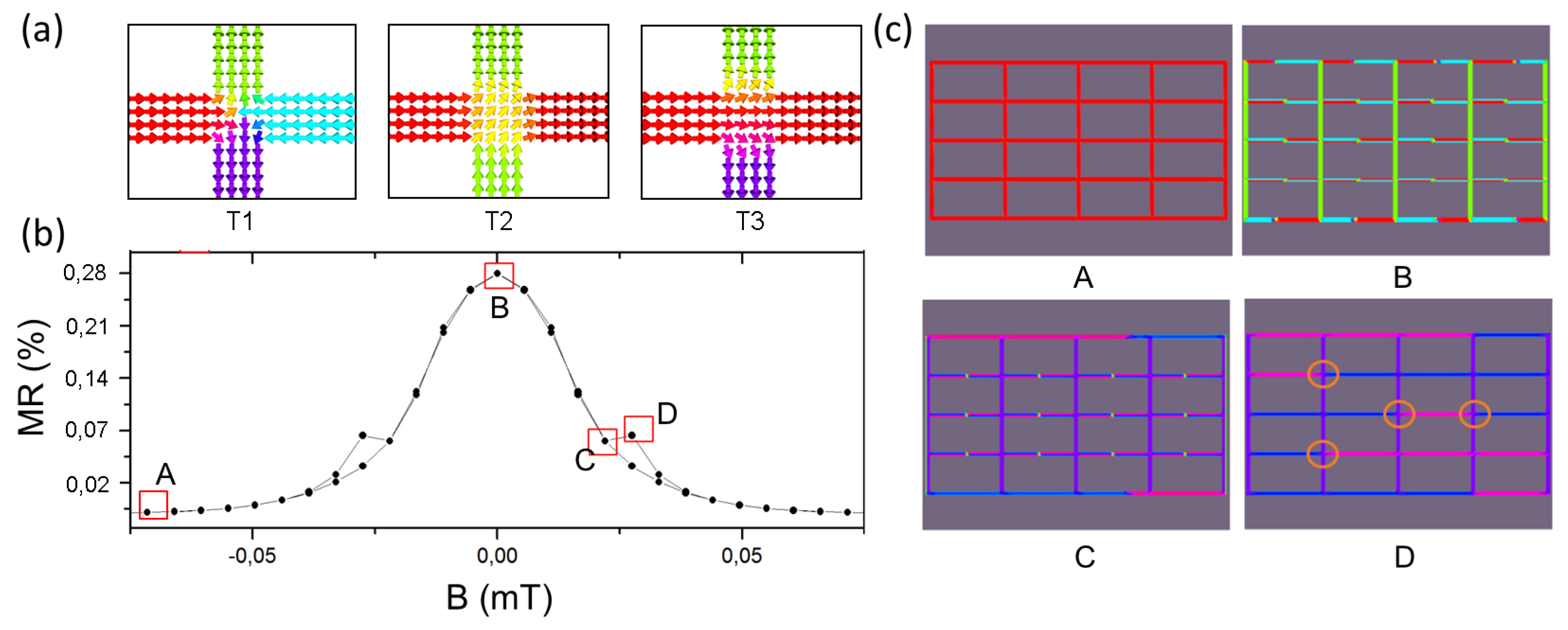
In order to better understand the magnetization reversal processes under an external magnetic field in those samples, we performed micromagnetic simulations following the procedure described in the Methods section. In
Figure 5a, we present the three main vertex configurations possible to be found during the MR process. These configurations are related to the ground state topology T1 in regular ASI samples, first excited state T2 and emergent monopole excitation T3. In connected samples, the monopole-like excitation is not present. Once the stray fields resembling magnetic monopoles are constricted to the sample plane, however, the respective characteristic domain walls could also be interestingly utilized in information technology or in memristive devices [
15], for example.
In
Figure 5b, we present the MR obtained after simulation iteration with Equation (
2). A qualitative match with the experimental results is verified, allowing the understanding of the origin of smaller peaks (pointing down). The disparities in the coercive field and saturation field values between the experimental and theoretical MR could be attributed to the defects in the experimental samples, not considered in simulation, which would provide magnetostatic traps to magnetization reversal. Another fact to be considered is that the saturation takes place earlier in the simulations due to the lower number of nanowire branches utilized for suitable simulations.
With the snapshots of simulations related to the most important points in the MR curve, we could conclude that the smaller resistance at magnetization saturation (point A) is related to the total uniformity in the product between current and magnetization in Equation (
2). In the opposite way, larger resistance is observed at zero field (point B), with the domain wall formation during magnetization reversal in nanomagnets perpendicular to the magnetic field, stimulated by the internal characteristic sample magnetic frustration. At point C, the resistance drops once some nanomagnets are already flipped, but returns to increase at point D with the formation of the T3 configuration, which could be related to the magnetic texture, similar to the configuration of magnetic monopole formation in non-connected ASIs. Sketches of the configurations at each point can be seen in
Figure 5c.
4. Conclusions
In this work, we have presented an alternative for fast and low-cost production as a good solution for athermic ASI sample development aligned with commercial production lines in clean-room laboratories. Together with the electrical contact electrodeposition, we have presented a full electrochemical route for nanomagnetic device production. This was just possible with the implementation of a pulsed potentiostatic deposition and environmental wettability improvement protocol. We have shown by SEM characterizations that without such a protocol it was impossible to achieve uniform nanomagnet films with small grains and complete geometry architecture transference to the samples. Through MFM images, we conclude that in samples made without the proposed protocol it was not possible to characterize nanomagnets with uniform magnetization in the whole sample, the condition needed for ASI lattices’ further characterization.
With MR measurements performed in good-quality connected samples and the support of micromagnetic simulations, we could indirectly corroborate the degeneracy recovered in the square connected lattice. The small peaks recorded at a lower field in Q samples suggest the very fast formation and annihilation of T3 magnetic textures, which is consistent with low-energy strings attaching to them. Surprisingly, the highest energy needed for T3 texture formation and annihilation was observed in the rectangular geometry R3, which is the one presenting the same distances between vertical opposed and diagonal nanomagnets, the condition needed for degeneracy observed in rectangular non-connected ASIs. The same behavior was observed with higher resistance and lower MR for that geometry. The consistency of our findings is corroborated by the subsequent decrease in the coercivity for the R4 geometry, evidence that coercivity is not necessarily proportional to the spacing of the lattice; rather, it is an individual characteristic of each geometry, favoring different texture formation at each lattice’s vertices. In this aspect, the behavior of sample R4 resembles that of a one-dimensional lattice once the distance of transversal wires could hide the characteristic system frustration.


