Abstract
In this work, we synthesized solutions of un-doped ZnO and ZnO doped with tin (Sn) by the sol-gel method. From these solutions, we deposited thin layers on glass substrates by the spin-coating technique. The main purpose of this work is to study the influence of the incorporation of Sn into the ZnO matrix on the photocatalytic properties of the latter. The crystal structure is hexagonal with a preferential orientation of the crystallites (002), and the reduction in the size of the grains is observed from 21 nm for the un-doped ZnO to 15 nm for the doped ZnO. For both samples, the transparency in the visible region is high and exceeds 75%, and a slight change in the band gap is from 3.22 to 3.23 eV, i.e., it is attributed to a combination of the Burstein–Moss effect and electron-impurity scattering. The methylene blue UV photocatalysis test gives a degradation rate of 40% for un-doped ZnO and 60% for Sn-doped ZnO (2%). This study confirms the remarkable influence of Sn doping on the photocatalytic properties of ZnO and also on its morphological and optical properties.
1. Introduction
Photocatalysis is of significant practical interest to intensive research efforts to develop new photocatalyst materials to improve pollutant degradation efficiency. Various semiconductor materials are considered as photocatalytic materials, such as CdS, ZnO, TiO2, Bi2O3, etc. [1,2]. The most commonly used semiconductor materials are TiO2 and ZnO. Due to these good characteristics and its exceptionally high UV absorption from the solar spectrum, ZnO is considered one of the best oxide photocatalysts. Zinc oxide is a binary Group II-VI semiconductor in the intrinsic state that is an n-type semiconductor with a hexagonal wurtzite structure, wide direct bandgap (3.3 eV), high energy exciton binding (60 meV) at 300 K, high carrier mobility, and high transparency in the visible spectrum. These properties make ZnO a favorite material for a wide range of applications such as UV lasers/detectors, UV detectors, field effect transistors, the surfaces of dye-sensitized solar cells, lighting applications, gas sensors, and photocatalysis [3]. Due to its advantages, its chemical stability, non-toxicity, simplicity of preparation, and low cost, ZnO is suggested as one of the preferred photocatalysts in the industrial field, To modify the properties (structural, morphological, optical, and electrical) of materials, there are several techniques. Among them, we find that doping by a wide range of metallic dopants, such as Ga, Al, In, and Sn, improves the photocatalytic properties of ZnO [4].
Several studies were carried out and proved to be the best under the photocatalytic activity of Sn-doped ZnO (regardless of the method of preparation) under UV irradiation. The work of Li et al. proved the photocatalytic properties of Sn-doped ZnO with different doping concentrations. In their study, Li et al. found that doping by a concentration of 1% gave good photocatalytic characteristics for ZnO concentrations [5]. Research has shown morphological changes in ZnO with changing doping and its concentration. In their study, Jia et al. observed increased methyl orange degradation by UV irradiation for Sn-doped ZnO (repaired by solid state reaction technique at room temperature) compared to un-doped ZnO [6]. In this work, thin layers of ZnO-Sn were developed by the spin-coating technique and their structural, morphological, optical and photocatalytic properties were verified. According to our best information about the published works on photocatalysis, which is very broad field, the spin-coating method is chosen because of its excellent advantages over other film deposition technique [7].
2. Experimental
Thin layers of pure and Sn-doped ZnO were deposited by spin coating. The raw materials were zinc acetate dihydrate (Zn(CH3COO)2·2H2O) as a precursor material, tin chloride (SnCl2) as a dopant, ethanol (C2H5OH) as a solvent, and monoethanolamine (C2H7NO) as a stabilizer. The working protocol is reported in reference [8]. Finally, the prepared layers were annealed for 1.5 h at a temperature of 500 °C in a Nabertherm muffle furnace. The prepared layers had a thickness of about 200 nm. The study of the crystalline structures of the layers was made by a Bruker D8 Advance X-ray diffractometer, with the use of a CuKα X-ray source (λ = 1.54 Å). The study of the transmission in the visible spectrum of our samples was carried out by a UV/visible Thermo spectrometer. For the observation of the surface morphology of the layers, we used a JEOL JSM-6610LA scanning electron microscopy (SEM) model. A Bruker SENTERRA R200L spectrometer was used to record the Raman spectra of our samples.
Photocatalytic Measurements
To verify the photocatalytic activities of our samples, we studied the degradation of methylene blue (MB) by UV light sources and fluorescent lamps. About the experimental conditions, the un-doped ZnO and Sn-doped ZnO catalyst (deposited on glass substrates) were immersed in an aqueous solution of methylene blue (MB) (15 mL) with a concentration of 1 × 10⁻⁴ M. It started with a magnetic agitation of 30 min and a light of 120 mtr/min. The radiation source used was a UV lamp. In this experiment, the lamp used was a Philips GT 15 w, producing UV light of 253 nm. This lamp was placed above the substrate at a distance of 10 cm. The calculation of the rate (percentage) of photodegradation of the MB solutions was made by the following formula [9]:
where At is the absorbance after time t, and A0 is the initial dye concentration before fading.
3. Results and Discussion
3.1. Structural Proprieties
In Figure 1, we show the X-ray diffraction patterns found for un-doped and Sn-doped ZnO. These diffractograms confirm a hexagonal wurtzite crystal system for our films [10]. The observed X-ray patterns clearly indicate that the un-doped and Sn-doped ZnO films exhibit good crystalline natures. The diffractograms of the un-doped and Sn-doped ZnO obtained confirm the good crystallization of the latter. Sn doping decreases preferential peak (002) intensity. Compared to the previous report [11], no other reflection peaks from impurities, such as other Sn oxides, are detected, indicating high purity of the Sn-doped ZnO product. Our results give a good crystallinity. These results confirm the better quality of the thin layers obtained. Calculations of the interplanar distance of un-doped and Sn-doped ZnO were made by Bragg’s relation [11]; the results found are displayed in Table 1:
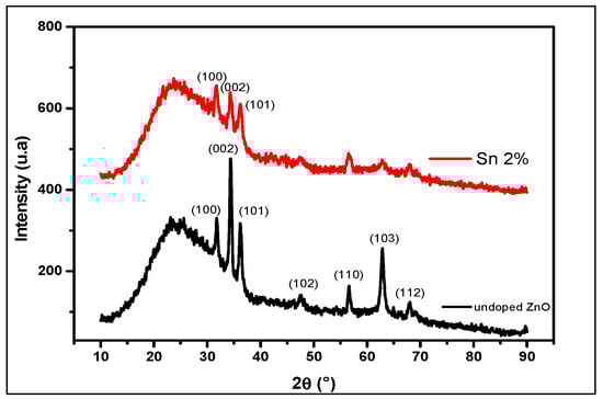
Figure 1.
XRD diagram of un-doped and 2% Sn-doped ZnO thin films.

Table 1.
Structural parameters.
Grain Size
The average crystallite size of ZnO was estimated according to the Debye–Scherrer formula [10]:
where “D” is crystallite size, λ is the X-ray wavelength used, β is the “full width at half maximum (FWHM)” of the diffraction peak, and θ is the angle measured (Braggs’ angle). The values obtained for the crystallites of the films are given in Table 1.
According to the table, a reduction in the size of the crystallites is observed between the undoped ZnO and the 2% Sn-doped ZnO from 21.69 nm to 15.78 nm. This decrease is due to the effect of the ionic radius of Sn4+ (RSn4+ = 0.071 nm), which is lower than that of Zn2+ (RZn2+ = 0.074 nm). Crystallite size varies with Sn doping, and this variation can be attributed to the disorder of the lattice at the pellets due to the difference between the ionic radii of ZnO and Sn [11,12]. For the hexagonal crystal, the calculations of the lattice parameters are given by relation (3) [13]:
A slight increase in unit cell parameters was observed with doping by Sn. Possibly, this may occur due to the strong covalent bond in the a-b plane and the difference in ionic radii between the Zn2+ and Sn4+ ions.
3.2. Morphological Properties
Figure 2 presents the SEM images of the layers of un-doped and Sn-doped ZnO, deposited by spin coating from a solution produced by the sol-gel method. For the observation of the morphologies of the surfaces of the films, we used a scanning electron microscope (SEM), and the latter provided us with a large amount of information on the surfaces of undoped ZnO and ZnO doped with 2% Sn. The observed images show that the surfaces are continuous, dense, and made up of spherical-shaped nanoparticles [14].
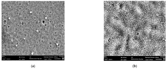
Figure 2.
SEM images of thin films of (a) = undoped and (b) ZnO doped with 2% Sn.
3.3. Optical Characterization
3.3.1. UV-Visible
The optical transmission spectra of un-doped and 2% Sn-doped ZnO thin films are shown in Figure 3. It is observed that the transmittance is good for the two films, and the latter varies between 75 to 96% in the visible spectrum (between 350 and 800 nm of the optical spectrum). The transparency of thin films increases with Sn doping. This increase is associated with the structural homogeneity and good crystallization of the prepared.
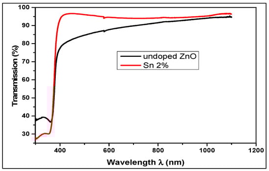
Figure 3.
Transmission curves of un-doped and Sn-doped ZnO thin films.
3.3.2. Determination of the Optical Gap
The optical band gap Eg is obtained by extrapolating the linear part of the graph (αhν)2 with respect to (hν) to α = 0, according to the following equation [15]. It is shown in Figure 4:
where hν is the photon energy, Eg is the band gap, and A is the absorption edge parameter. The “n” was taken equal to 1/2 because the deposited material had a direct band gap.
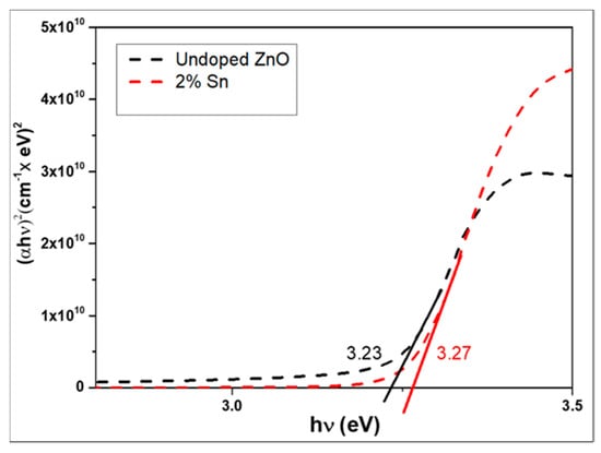
Figure 4.
Optical bandgap plots for un-doped ZnO and Sn-doped ZnO thin films.
The optical band gap increased slightly when doped with Sn, and the gap values of the un-doped and doped ZnO layers were 3.22 3.23 and 3.23 3.27 eV, respectively. This increase may have been due to the increased carrier concentration introduced by Sn doping, known as the Moss–Burstein effect [16]. The presence of Sn impurities in the ZnO crystal lattice induced new recombination centers with lower emission energies, thus reducing the bandgap energy [17].
3.4. Raman Spectroscopy
Figure 5 shows the thin layer of the Raman spectra of the un-doped and Sn-doped ZnO obtained by the spin-coating technique. We observe two small peaks around 109 cm−1 and 439.5 cm−1, respectively, representing the two active modes 𝐸2Low and 𝐸2High [18], and these are typical Raman peaks of ZnO. Two predominant peaks, one at 560–562 cm−1, of the E1(LO) mode are caused by the defects of the oxygen O vacancy, Zn-interstitial defect states, or these complexes and free carriers [19]. Researchers have suggested that these modes relate to modes induced by point defects and can be used as indicators to verify the incorporation of dopants introduced into the host matrix. These results obtained from RAMAN were consistent with the results from XRD, where both samples contained ZnO in the crystalline phase. We also noted the absence of any SnO band in the Raman spectrum [20].
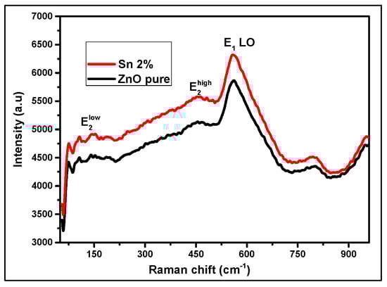
Figure 5.
Raman spectra of un-doped and Sn-doped ZnO thin films.
3.5. Photocatalysis
The photocatalytic activities of un-doped and Sn-doped ZnO prepared with various concentrations were tested for the degradation of methylene blue (MB) under UV light illumination, as shown in Figure 6. In the figure, we see that the absorption peak of the methylene blue (MB) solution at 554 nm decreased along with other small peaks, which were also decreased, indicating the decolorization process. All the samples revealed a common trend, i.e., the concentration of methylene blue MB gradually decreased with the lengthening of the irradiation time. Under irradiation, ZnO absorbs photons and generates electrons and holes. Figure 6a,b demonstrated the enhancement of the photocatalytic performances of the ZnO thin films by Sn doping and also accelerated the photodegradation reaction process [21].
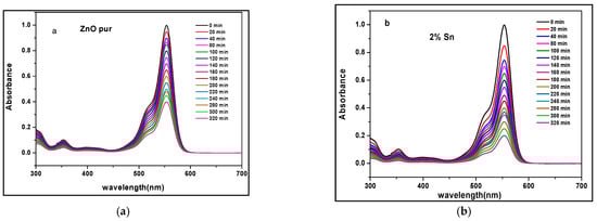
Figure 6.
UV-Vis absorption spectra of (a) un-doped ZnO and (b) Sn-doped ZnO thin film for MB degradation at different times.
The variation in the absorbance of methylene blue was plotted as a function of exposure time (Figure 7). With an efficient dye photodegradation, it was observed that there was an increasing tendency for degradation faster than un-doped ZnO for the Sn-doped ZnO sample.
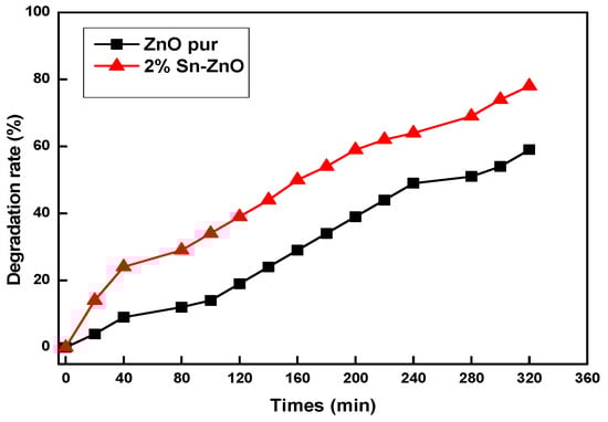
Figure 7.
MB dye degradation rate at different UV irradiation times using ZnO and Sn-ZnO films treated at 500 °C.
4. Conclusions
The thin layers of un-doped and Sn-doped ZnO were deposited by the spin-coating technique. In this work, we studied the variations in the structural, optical, morphological, and photocatalytic properties of ZnO layers by the addition of Sn doping. For the two samples, ZnO un-doped and ZnO doped Sn, it was shown that the structures comprised hexagonal wurtzite with preferential orientations according to (002). The microstructures of the two samples (ZnO doped Sn at 2% and un-doped ZnO) turned out to be quite similar with the presence of spherical grains. Given that the optical transmission was 75% within the visible region, Sn doping gave excellent transparency in the visible range for ZnO and an optical gap in the order of 2.23 eV. The results indicated the possibility of the application of un-doped ZnO and ZnO-Sn (2%) as photocatalysts for the photodegradation of methylene blue.
Author Contributions
F.B., R.Z., M.-C.B., H.D., F.L. and N.B. participated in this work because it is the work of a research team. All authors have read and agreed to the published version of the manuscript.
Funding
This research received no external funding.
Institutional Review Board Statement
Not applicable.
Informed Consent Statement
Not applicable.
Data Availability Statement
Not applicable.
Conflicts of Interest
The authors declare no conflict of interest.
References
- Pandiyan, R.; Dharmaraj, S.; Ayyaru, S.; Sugumaran, A.; Somasundaram, J.; Kazi, A.S.; Samiappan, S.; Ashokkumar, V.; Ngamcharussrivichai, C. Ameliorative photocatalytic dye degradation of hydrothermally synthesized bimetallic Ag-Sn hybrid nanocomposite treated upon domestic wastewater under visible light irradiation. J. Hazard. Mater. 2022, 421, 126734. [Google Scholar] [CrossRef] [PubMed]
- Kaus, H.M.; Rithwan, F.; Adnan, R.; Ibrahim, L.; Thongmee, S.; Yusoff, M. Effective Strategies, Mechanisms, and Photocatalytic Efficiency of Semiconductor Nanomaterials Incorporating rGO for Environmental Contaminant Degradation. Catalysts 2021, 11, 302. [Google Scholar] [CrossRef]
- Ganesh, V.; Yahia, I.S.; AlFaify, S.; Shkir, M. Sn-doped ZnO nanocrystalline thin films with enhanced linear and nonlinear optical properties for optoelectronic applications. J. Phys. Chem. Solids 2017, 100, 115–125. [Google Scholar] [CrossRef]
- Lin, J.; Mo, L.; Xu, S.; Wei, Q.; Fu, Y.; Lin, X.; Xiao, X. Unlocking photoredox selective organic transformation over metal-free 2D transition metal chalcogenides-MXene heterostructures. J. Catal. 2020, 391, 485–496. [Google Scholar] [CrossRef]
- Roguai, S.; Djelloul, A. Photocatalytic degradation of methylene blue using sprayed Mg diluted ZnO heterostructure thin films photocatalysts, Reaction Kinetics. Mech. Catal. 2021, 132, 1225–1244. [Google Scholar]
- Wang, J.; Pan, H.; Xu, X.; Jin, H.; Ma, W.; Xiong, S.; Bao, Q.; Tang, Z.; Ma, Z. Li-Doped ZnO Electron Transport Layer for Improved Performance and Photostability of Organic Solar Cells. ACS Appl. Mater. Interfaces 2022, 14, 12450–12460. [Google Scholar] [CrossRef] [PubMed]
- Patil, N.B.; Nimbalkar, A.R.; Patil, M.G. ZnO thin film prepared by a sol-gel spin coating technique for NO2 detection. Mater. Sci. Eng. B 2018, 227, 53–60. [Google Scholar] [CrossRef]
- Boufelgha, F.; Brihi, N.; Labreche, F.; Guendouz, H.; Barbadj, A. Enhanced of blue and green emission by Ce–ZnO thin films prepared by sol–gel technique. Semiconductors 2022, 56, 275–280. [Google Scholar] [CrossRef]
- Abbas, F.; Bensaha, R. Effect of annealing time on structural and optical proprieties of mercury (Hg+2) doped TiO2 thin films elaborated by sol-gel method for future photo-catalytic application. Opt. Int. J. Light Electron Opt. 2021, 247, 167846. [Google Scholar] [CrossRef]
- Venkatesh, N.; Aravindan, S.; Ramki, K.; Murugadoss, G.; Thangamuthu, R.; Sakthivel, P. Sunlight-driven enhanced photocatalytic activity of bandgap narrowing Sn-doped ZnO nanoparticles. Environ. Sci. Pollut. Res. 2021, 28, 16792–16803. [Google Scholar] [CrossRef]
- Sarica, E.; Gunes, I.; Akyuz, I.; Bilgin, V.; Erturk, K. Sol-gel derived ZnO:Sn thin films and fabrication of n-ZnO:Sn/p-Si heterostructure. Opt. Mater. 2021, 118, 111283. [Google Scholar] [CrossRef]
- Özgür, Ü.; Alivov, Y.I.; Liu, C.; Teke, A.; Reshchikov, M.A.; Doğan, S.; Avrutin, V.; Cho, S.-J.; Morkoç, H. A comprehensive review of ZnO materials and devices. J. Appl. Phys. 2005, 98, 041301. [Google Scholar]
- Ajili, M.; Castagné, M.; Turki, N.K. Study on the doping effect of Sn-doped ZnO thin films. Superlattices Microstruct. 2013, 53, 213–222. [Google Scholar] [CrossRef]
- Verma, M.; Dwivedi, P.K.; Das, B. Structure–property correlation of pure and Sn-doped ZnO nanocrystalline materials prepared by co-precipitation. J. Exp. Nanosci. 2015, 10, 438–448. [Google Scholar] [CrossRef]
- Dhamodharan, P.; Manoharan, C.; Dhanapandian, S.; Bououdina, M.; Ramalingam, S. Preparation and characterization of spray deposited Sn-doped ZnO thin films onto ITO subtracts as photoanode in dye sensitized solar cell. J. Mater. Sci. Mater. Electron. 2015, 26, 4830–4839. [Google Scholar] [CrossRef]
- Moss, T.S. The Interpretation of the Properties of Indium Antimonide. Proc. Phys. Soc. B 1954, 67, 775–782. [Google Scholar] [CrossRef]
- Andolsi, Y.; Chaabouni, F.; Abaab, M. Sn doping effects on properties of ZnO thin films deposited by RF magnetron sputtering using a powder target. J. Mater. Sci. Mater. Electron. 2017, 28, 8347–8358. [Google Scholar] [CrossRef]
- Horzum, S.; Bulduk, E.; Şener, D.; Serin, T. Comparison of characteristic properties of Al, Ga, and In-doped ZnO thin films formed by sol-gel method. Superlattices Microstruct. 2021, 159, 107034. [Google Scholar] [CrossRef]
- Rajalakshmi, M.; Arora, A.K.; Bendre, B.S.; Mahamuni, S. Optical phonon confinement in zinc oxide nanoparticles. J. Appl. Phys. 2000, 87, 2445–2448. [Google Scholar] [CrossRef]
- Pradhan, A.K.; Zhang, K.; Loutts, G.; Roy, U.N.; Cui, Y.; Burger, A. Structural and spectroscopic characteristics of ZnO and ZnO:Er3+ nanostructures. J. Phys. Condens. Matter 2004, 16, 7123–7129. [Google Scholar] [CrossRef]
- Shah, A.A.; Bhatti, M.A.; Tahira, A.; Chandio, A.D.; Channa, I.A.; Sahito, A.G.; Chalangar, S.E.; Willander, M. Omer Nur and Zafar Hussain Ibupoto, Facile synthesis of copper doped ZnO nanorods for the efficient photo degradation of methylene blue and methyl orange. Ceram. Int. 2020, 46, 9997–10005. [Google Scholar] [CrossRef]
Disclaimer/Publisher’s Note: The statements, opinions and data contained in all publications are solely those of the individual author(s) and contributor(s) and not of MDPI and/or the editor(s). MDPI and/or the editor(s) disclaim responsibility for any injury to people or property resulting from any ideas, methods, instructions or products referred to in the content. |
© 2023 by the authors. Licensee MDPI, Basel, Switzerland. This article is an open access article distributed under the terms and conditions of the Creative Commons Attribution (CC BY) license (https://creativecommons.org/licenses/by/4.0/).