
Review

A New Era in Computing: A Review of Neuromorphic Computing Chip Architecture and Applications

1
Micro-Nano Electronics Building, Peking University, Beijing 100871, China
2
Hunan Water Resources and Hydropower Survey, Design, Planning and Research Co., Ltd., Changsha 410007, China
3
School of Artificial Intelligence and Data Science, University of International Business and Economics, Beijing 100029, China
4
School of Computer Science and Engineering, Beihang University, Beijing 100191, China
*
Author to whom correspondence should be addressed.
Submission received: 17 October 2025 / Revised: 1 December 2025 / Accepted: 16 January 2026 / Published: 22 January 2026

Abstract

Neuromorphic computing, an interdisciplinary field combining neuroscience and computer science, aims to create efficient, bio-inspired systems. Different from von Neumann architectures, neuromorphic systems integrate memory and processing units to enable parallel, event-driven computation. By simulating the behavior of biological neurons and networks, these systems excel in tasks like pattern recognition, perception, and decision-making. Neuromorphic computing chips, which operate similarly to the human brain, offer significant potential for enhancing the performance and energy efficiency of bio-inspired algorithms. This review introduces a novel five-dimensional comparative framework—process technology, scale, power consumption, neuronal models, and architectural features—that systematically categorizes and contrasts neuromorphic implementations beyond existing surveys. We analyze notable neuromorphic chips, such as BrainScaleS, SpiNNaker, TrueNorth, and Loihi, comparing their scale, power consumption, and computational models. The paper also explores the applications of neuromorphic computing chips in artificial intelligence (AI), robotics, neuroscience, and adaptive control systems, while facing challenges related to hardware limitations, algorithms, and system scalability and integration.

1. Introduction

Neuromorphic computing, an interdisciplinary field at the intersection of neuroscience, computer engineering, and artificial intelligence, has emerged as a promising paradigm for building energy-efficient, brain-inspired computing systems. Unlike traditional Von Neumann architectures, which separate memory and processing units, neuromorphic systems integrate memory with processing, enabling efficient, parallel, and event-driven computation. Neuromorphic computing chips simulate the behavior of biological neurons, synapses, and neural networks, making them well-suited for tasks that involve pattern recognition, sensory processing, and decision-making. These systems operate in a manner analogous to the human brain, with the potential to drastically improve the performance and energy efficiency of artificial intelligence (AI) algorithms.
Traditional computing architectures, based on the von Neumann model, face limitations when tasked with processing complex, real-time, and large-scale AI workloads. The von Neumann architecture is characterized by its sequential processing and separate memory and computation units, which often lead to bottlenecks and high power consumption. In contrast, neuromorphic computing systems are designed to address these issues by mimicking the parallelism, feedback loops, and adaptability of biological neural networks [1]. The neuromorphic approach is particularly suitable for tasks requiring high parallelism, such as deep learning and reinforcement learning, which have emerged as the backbone of many modern AI applications [2,3]. Table 1 compares the two main branches of computing architectures.
This review aims to provide a comprehensive overview of neuromorphic computing chips, focusing on their architecture, applications, and the latest advances in hardware and algorithms. First, it provides a detailed examination of the underlying principles that distinguish neuromorphic systems from traditional computing models, such as event-driven processing, spiking neural networks (SNNs), and the use of non-volatile memory technologies. Second, it surveys the latest hardware implementations, including custom-designed chips such as IBM’s TrueNorth and Intel’s Loihi, and explores their strengths, limitations, and potential for scaling. Third, this paper presents a critical discussion of the current state of neuromorphic algorithms, particularly in the context of their application to real-world problems such as robotics, sensory processing, and AI decision-making. Finally, the review proposes future directions for research, focusing on key challenges such as improving network connectivity, enhancing energy efficiency, and achieving seamless integration of neuromorphic systems into existing AI workflows. Table 2 lists the comparison of the key features with relevant review papers.
Compared to prior reviews that focus on either hardware or algorithms in isolation, this work provides (1) a unified analysis of digital, hybrid, and memristor-based implementations using a novel five-dimensional framework; (2) a re-categorized taxonomy of hybrid architectures that clarifies the distinction between analog and digital components; and (3) the first systematic discussion of perception–computation–action closed-loop systems as a distinct application domain.
The rest of this paper is structured as follows: Section 2 covers the fundamentals of neuromorphic computing, including spiking neurons, network topologies, and key differences from traditional architectures such as pulse-based processing, parallelism, and event-driven computation; Section 3 discusses various implementations of neuromorphic chip architectures, including digital-only implementations, and hybrid analog–digital designs, with examples like BrainScaleS and other systems. In Section 4, we explore practical applications of neuromorphic computing in areas like robotics, AI, and brain-machine interfaces; Section 5 identifies the major technical and engineering challenges in scaling neuromorphic systems, including hardware limitations and software integration. In Section 6, we conclude with a discussion of the future of neuromorphic computing, potential research directions, and the impact of emerging technologies in this field.

2. Background

2.1. Spiking Neural Networks

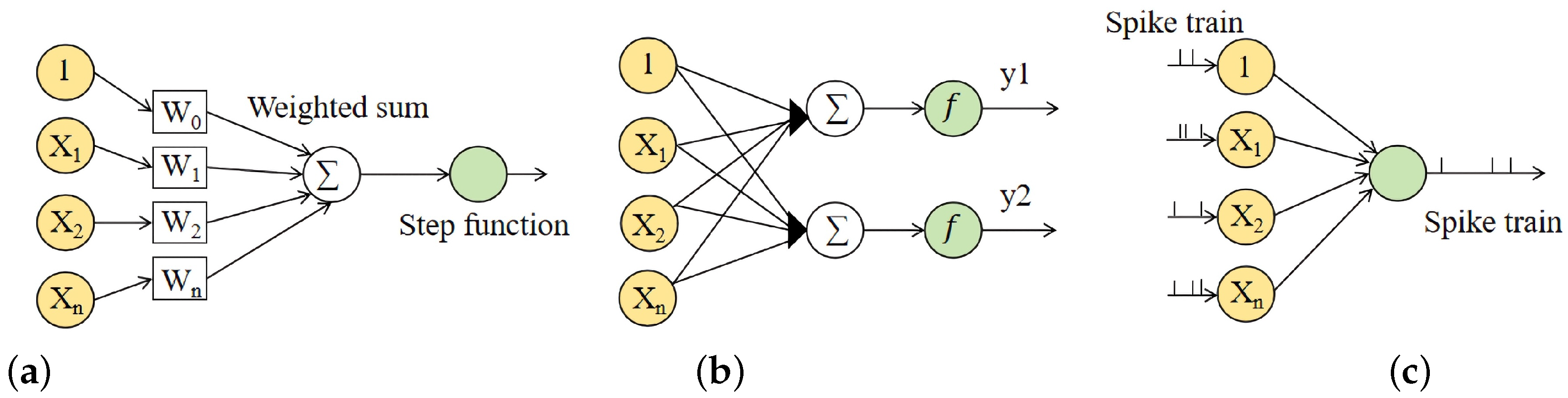
Spiking neural networks (SNNs) represent the third generation of artificial neural networks, designed to emulate the information processing mechanisms found in biological neural systems, specifically [7], neuromorphic computing. Compared to previous generations, their functionality is more closely approximated than that of the mammalian brain. They were first proposed by researchers from Heidelberg University and the University of Bern [8] as a fast and energy-efficient technology that performs computations using spiking neuromorphic substrates. Unlike traditional artificial neural networks (ANNs), SNNs communicate through discrete spike signals, analogous to action potentials in biological neurons, thereby endowing them with greater biological plausibility and enhanced spatiotemporal processing capabilities. Consequently, SNNs serve as a promising class of models for simulating the dynamics of brain neurons. Figure 1 illustrates the three generations of chips.

2.1.1. Spiking Neurons

SNNs utilize spiking neurons as computational units, emulating the information encoding and processing mechanisms of the human brain. Given the dynamic characteristics of neuronal membrane potentials, neuroscientists have developed various spiking neuron models over the years, which define the fundamental dynamics of SNNs. Among the most influential models are the Hodgkin–Huxley (H-H) model, the Leaky Integrate-and-Fire (LIF) model, the Spike Response Model (SRM), the Izhikevich model, and the Memristive Izhikevich model.
(1)
Hodgkin–Huxley Model:
In 1952, Hodgkin and Huxley conducted pioneering research on the mechanisms underlying the initiation and propagation of action potentials in neurons. They developed a mathematical model that describes the relationship between membrane current and membrane potential, which has come to be known as the Hodgkin–Huxley (H-H) model. Their seminal work elucidating the generation and propagation of action potentials earned them the Nobel Prize in Physiology or Medicine in 1963.
The H-H model provides the most biologically accurate description of neuronal properties and is extensively utilized in computational neuroscience. Although conductance-based models incorporating ion channel dynamics elucidate the emergence of neuronal spikes and provide a more detailed biological description, they obscure the prioritization of different degrees of freedom within a single neuron, thereby complicating the clear understanding of neuronal dynamics [9].
(2)
Leaky Integrate-and-Fire model
The Integrate-and-Fire (IF) model, originally proposed by Lapicque in 1907, serves as a fundamental framework for simulating neuronal behavior [10]. It describes the basic dynamics of neuronal membrane potential by accumulating input currents until a threshold is reached, at which point the neuron generates an action potential and the membrane potential is restored to a resting state. This model captures the essential behavior of neurons in generating electrical signals upon sufficient stimulation. Despite its simplicity, the IF model lays the groundwork for understanding neuronal electrical activity and inspires further developments in more biologically realistic models.
The Leaky Integrate-and-Fire (LIF) model is the most widely used model in SNNs, although it overlooks the dynamic changes in ion channels and only reflects the variations in the macroscopic membrane potential, resulting in simpler calculations.
(3)
Spike Response Model
The Spike Response Model (SRM) was first proposed by Gerstner et al., aiming to provide a simplified mathematical description of the spiking behavior of neurons. This model design not only simplifies the dynamic description of neurons but also significantly improves the computational efficiency, endowing it with great application potential in large-scale neural network simulations.
(4)
Izhikevich model
In the field of neuronal modeling, improving computational efficiency while preserving the biological properties of neurons has been a central issue of research. The Izhikevich model, as a simple and efficient neuronal model, successfully bridges a gap between the biophysical model (including the H-H model) and the abstract model (including the I-F Model). The model, proposed by Eugene M. Izhikevich in 2003 [11], aims to reproduce the dynamic behavior of multiple neurons in the form of minimalist equations because of its high efficiency and biological plausibility [12].
The advantage of IZH is its extremely high computational efficiency [13,14]. This high performance enables the Izhikevich model to simulate large-scale neural networks in real-time. Despite simplification, the Izhikevich model retains the basic biological properties of neurons, such as distribution, bursting, and frequency adaptation. By tuning the parameters, the model can simulate multiple types of cortical neurons.
Neuromorphic computing seeks to emulate the structure and function of biological nervous systems to enable efficient and low-power information processing. The Memristive Izhikevich model provides a more realistic simulation basis for neuromorphic computing by combining the dynamic properties of neurons and synapses. In addition to neuroscience, it is also used in signal processing, machine learning, hardware security, and other fields [15]. Its unique memory properties and neuronal dynamic behavior provide new perspectives and approaches to study in these fields. Table 3 compares several neuron models based on their features.

2.1.2. Topology of Neural Networks

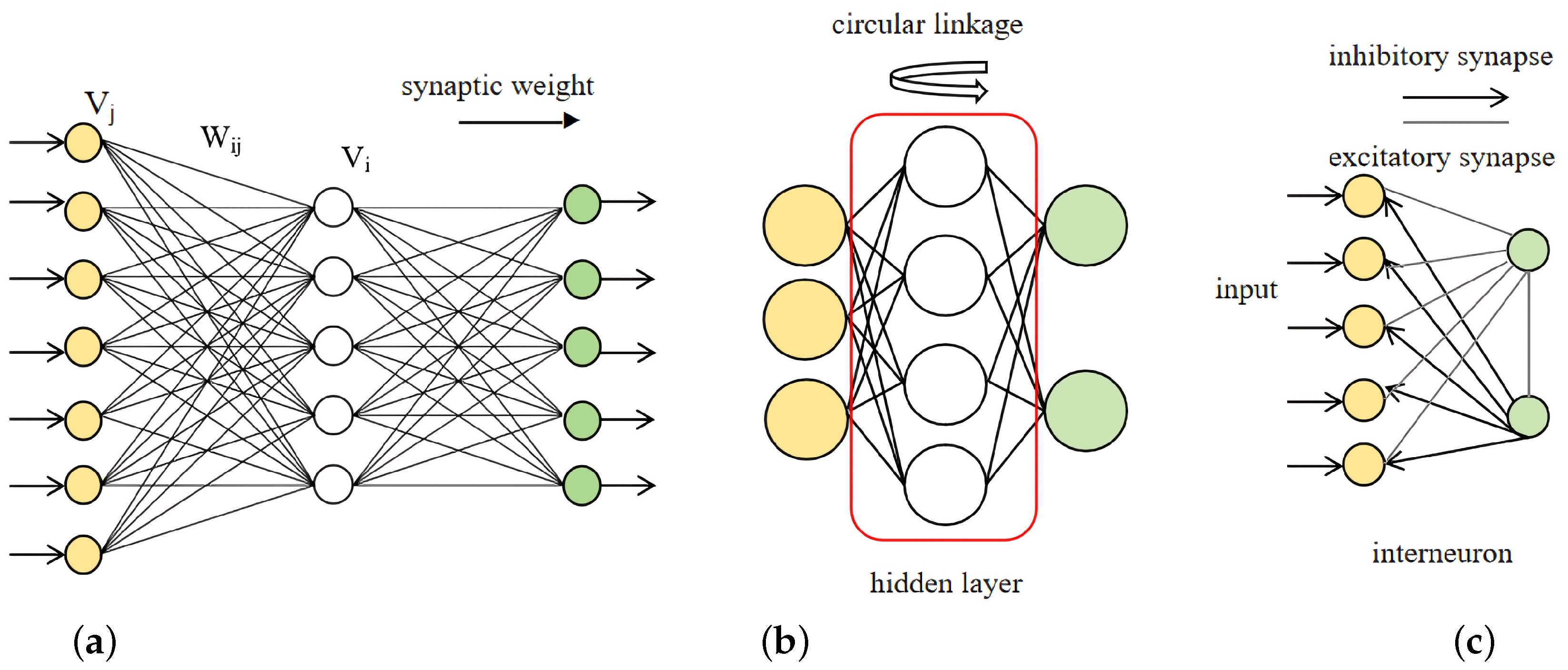
Multiple spiking neurons form large-scale SNNs through synaptic connections, with various connection types determining the network’s topology. Similarly to traditional ANNs, the topology of SNNs can be categorized into feedforward SNNs, recurrent and cyclic SNNs, and hybrid SNNs.
(1)
Feedforward SNNs
Feedforward SNNs represent the most fundamental topology structure. Their defining characteristic is the linear flow of information, which consists of an input layer, hidden layers, and an output layer. Each layer comprises one or more neurons, with synaptic connections between layers dynamically adjusted through multiple weights. Information flows from the input layer through the hidden layers to the output layer, with no direct feedback connections between neurons across different layers. This structure is straightforward and clear, making it easy to implement and train, particularly when handling static or fixed input data. By adjusting the synaptic weights and the time constants of the neurons, feedforward SNNs can learn the mapping relationship between inputs and outputs, which is suitable for fundamental machine-learning tasks such as classification and regression. Although they are relatively simple in structure, their expression ability and learning efficiency can be significantly improved by introducing mechanisms such as time coding and spike-timing-dependent plasticity (STDP). Feedforward SNNs are computationally stable and easy to train and are widely used in tasks such as image classification and speech recognition [16].
(2)
Recurrent and cyclic SNNs
Recurrent and cyclic SNNs are more complex than feedforward SNNs and can store historical information through recurrent connections, making them suitable for temporal data processing tasks, in particular speech modeling, motion prediction, and brain signal analysis [17], introducing the feedback mechanism that allows these networks to process dynamic inputs and maintain internal state, thus simulating short- and long-term memory capabilities of the biological neural system. Such networks show significant advantages in tasks that include processing sequence data, time series prediction, and reinforcement learning. Conversely, the introduction of feedback SNNs also brings challenges in algorithm design and training, including high computational complexity and issues, capturing long-term dependencies, etc. To address these issues, the researchers propose various strategies, particularly using long-term memory (LSTM) units, a gating mechanism, and spike-based temporal backpropagation.
(3)
Hybrid SNNs
Hybrid SNNs integrate the advantages of feedforward, recurrent and other structures, achieving more flexible and powerful information processing capabilities through local or global hybrid configuration. Different substructures are applied in different tasks to maximize the computational efficiency and biological fit. For instance, in computer vision tasks, local features can be processed using feedforward-type structures, while in time series modeling tasks, local circuits can be used to store historical information. The design challenge of hybrid SNNs lies in how to effectively fuse different types of subnets and how to achieve complex dynamic behavior while maintaining network efficiency. (see Figure 2).

2.2. Neuromorphic Hardware

Neuromorphic hardware is an innovative computing architecture that mimics the structure and function of biological nervous systems. Its goal is to achieve efficient, low-power information processing by replicating the behavior of neurons and synapses. Unlike traditional computing architectures, neuromorphic hardware employs spike signals for spatiotemporal coding, incorporating simulated neural activity, event-based computing, non-von Neumann architecture, and memory processing. These systems are designed for a diverse array of applications, spanning from neuroscience research to low-power edge intelligence and data center acceleration [18]. They have the capability to tackle complex tasks with greater parallelism and lower power consumption. This cutting-edge technology is increasingly finding its way into key areas such as healthcare, robotics, artificial intelligence, and the Internet of Things. In the medical field, neuromorphic hardware is skillfully applied to tactile prosthetics [19]. Accurately simulating biological neural activities brings natural and smooth tactile feedback and neural stimulation to users, which greatly improves the practicality and user experience of the prostheses. In the field of robotics, it helps robots achieve real-time perception and intelligent decision-making, enabling them to respond to and complete tasks quickly in complex and changing environments. Additionally, neuromorphic hardware demonstrates considerable potential and value in areas such as image recognition, speech processing, and edge computing. Table 4 compares features of the traditional and neuromorphic systems.
Compared with traditional computing architectures, neuromorphic systems show significant differences in multiple dimensions. Traditional computing architecture relies on binary digital signals serially, and data needs to be frequently transmitted between storage units and computing units. Namely, the central processing unit (CPU) performs a wide range of tasks, executing instructions and managing operations with its general-purpose processing capabilities. GPUs, originally designed for rendering images, have evolved to accelerate complex computations by performing the same operation on multiple pieces of data simultaneously, making them ideal for tasks like machine learning and scientific simulations. This separation of memory and computing in traditional designs leads to high power consumption and low efficiency. The neuromorphic systems use spike signals for spatiotemporal coding, simulate the working mode of biological neurons, and integrate memory and computation through parallel event-driven computing modes. This design not only improves computational efficiency but also significantly reduces energy consumption and breaks the bottleneck of traditional architecture.

2.2.1. Neuron Simulator

The neuron simulator is one of the core components of neuromorphic hardware, used to simulate the dynamic processes of biological neurons at the hardware level. This simulator realizes the accurate simulation of biological neuron behavior by simulating the characteristics of membrane potential accumulation and spike emission of neurons. For example, artificial neurons based on light-responsive two-dimensional materials can directly regulate capacitance properties through light spikes, realizing threshold triggering and frequency adaptation of biological-like neurons [20]. This design allows neuron simulators to perform well in applications including edge computing, efficiently processing complex neural signals, and delivering accurate computing results [21].

2.2.2. Neuromorphic Computing Chips

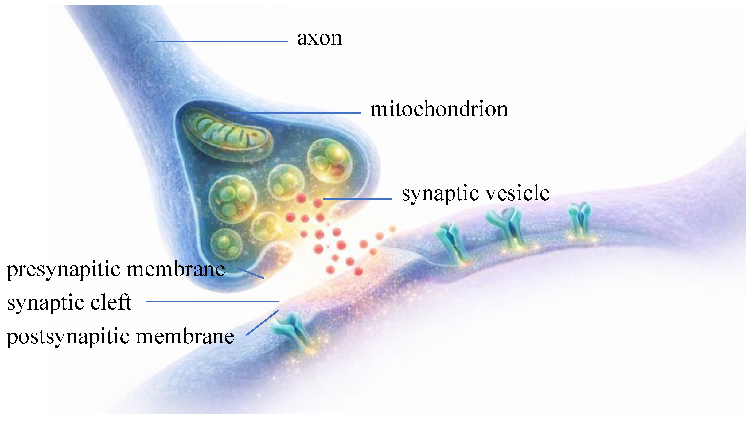
At the forefront of neuromorphic computing, brain-like chips offer remarkable computational efficiency and low power consumption. These innovative designs not only transcend the limitations of traditional computing architecture but also herald transformative changes across various domains, including artificial intelligence, biomedicine, and the Internet of Things. For example, the ROLLS chip is a reconfigurable online learning spiking neuromorphic processor equipped with 256 silicon neurons and 128K plastic synapses, capable of implementing spike-timing learning rules and allowing for real-time emulation of neural system dynamics [22] (see Figure 3).

2.2.3. Spiking Neural Networks Hardware

SNNs encode information through spike timing, which closely emulates the information transmission mechanism of the biological neural system, providing SNNs with a significant advantage in processing spatiotemporal information. However, these coding methods also impose higher demands on hardware, especially precise temporal synchronization to ensure accurate transmission and processing of spike signals. In recent years, researchers have made significant progress in hardware support. An instance shows that field-effect transistors (FETs) based on triboelectric potential modulation are proposed to simulate synaptic mechanical plasticity. This design not only enables the direct interaction between tactile signals and neural computation but also provides a new idea for the development of biomimetic robotic perception systems. Consequently, robots can sense and respond to changes in the external environment more naturally, thus showing greater adaptability in complex environments.

3. Neuromorphic Computing Chip Architecture

From 1990 to 2010, neuromorphic chips were primarily implemented using analog methods, with limited scale for neurons and synapses. With the advancement of integrated circuit technology, after 2010, large-scale mixed-signal implementations and pure digital implementations began to emerge. Neuromorphic computing chip implementations mainly include hybrid digital–analog implementations and purely digital implementations.

3.1. Digital–Analog Hybrid Implementation

We define hybrid neuromorphic architectures as systems that combine analog neuronal dynamics with digital communication and control. This includes chips where (1) neurons are implemented using analog or mixed-signal circuits; (2) synapses employ either analog or digital weight storage; and (3) spike routing utilizes digital packet-switched networks. This clarification ensures consistent categorization throughout our analysis.
The core design goal of neuromorphic computing chips is to simulate the computational mechanisms of the brain so as to replicate, as closely as possible, the dynamic processes of the biological nervous system at the hardware level. In order to achieve this goal, many chips use a hybrid digital–analog implementation. Digital–analog hybrids combine the advantages of analog and digital circuits in order to achieve massively parallel processing and dynamic learning capabilities at low power consumption. In this paper, we will introduce several representative neuromorphic computing chips, including BrainScaleS, Neurogrid, DYNAPs, and ROLLS, and discuss in detail their processes, neuron and synapse sizes, power consumption, on-chip architectures, on-chip network architectures, and in-core computational models, providing performance comparisons and a look at future trends.

3.1.1. Neurogrid

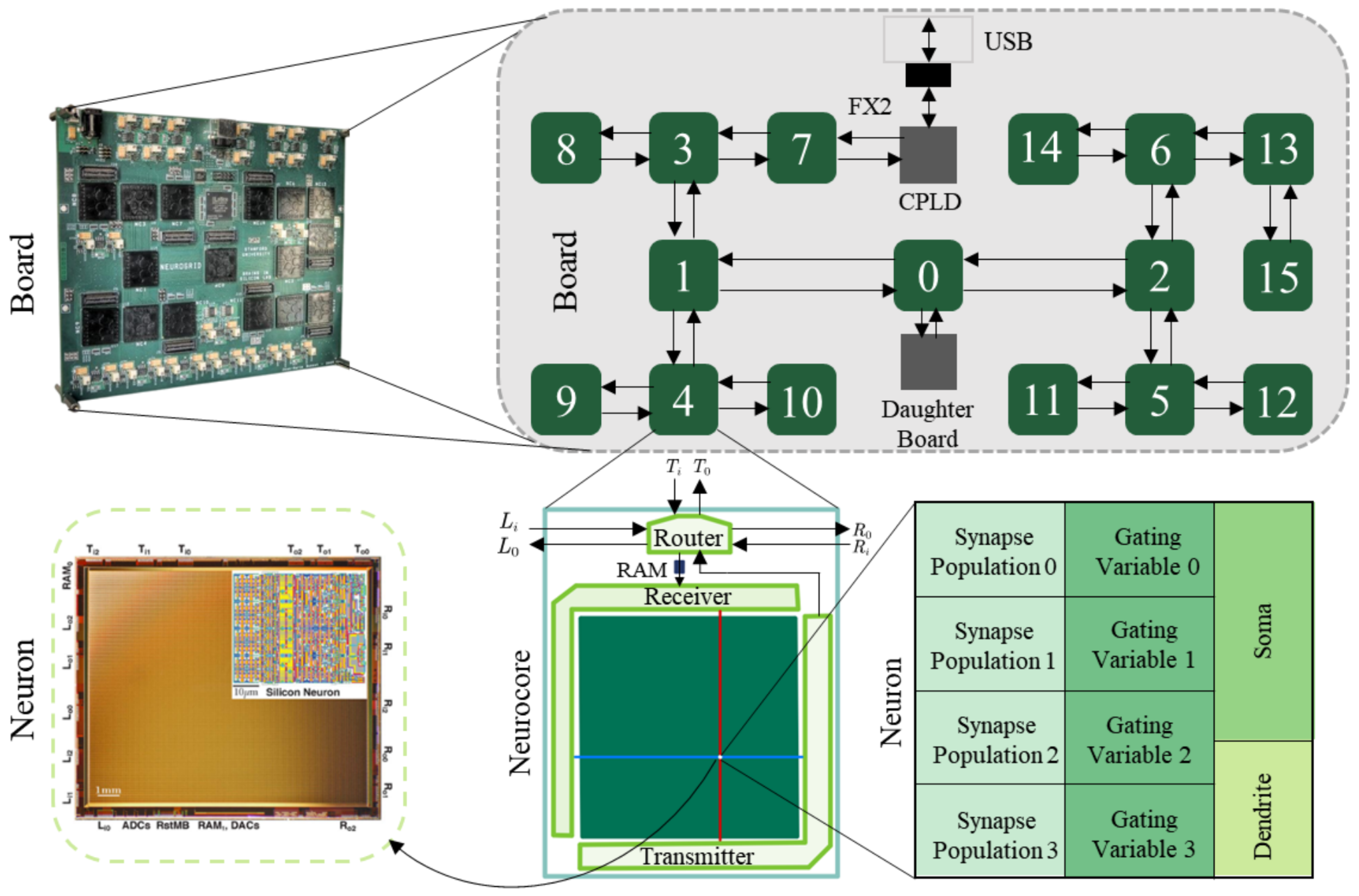
Neurogrid employs a pure analog architecture in 180 nm CMOS technology (see Figure 4), utilizing subthreshold circuits to achieve extreme energy efficiency. The platform simulates 1,048,576 neurons and billions of synapses with 5 W power consumption. Its design leverages time-division multiplexing to enable high synaptic density but is limited to static connectivity without plasticity capabilities, making it suitable for real-time brain emulation rather than adaptive applications. Neurogrid also has low power consumption. Its low-power design gives it a strong competitive edge in neuromorphic computing [23].
Neurogrid implements neurons and synapses using analog mixed-signal CMOS circuits. Neurons are realized via subthreshold operational transconductance amplifiers (OTAs), emulating biological membrane dynamics through capacitive integration and spike-triggered reset. Synapses employ programmable current sources controlled by DRAM-based weight storage cells. Charge maintenance on capacitors enables dynamic reconfiguration [24]. All components operate in the subthreshold region for ultra-low power consumption, utilizing standard CMOS processes without exotic materials.
The core neuron circuit integrates a membrane potential integrator, spike-generation comparator, and reset mechanism. Synaptic arrays combine weight storage DRAM cells with current-steering digital-to-analog converters that inject weighted currents upon presynaptic spiking. Event-driven operation ensures circuits activate only during spike events, while subthreshold biasing minimizes static power dissipation. Time constants are set by OTA transconductance and capacitance values.
A hierarchical address-event representation (AER) protocol interconnects components. Each of the 16 × 16 neurocores contains 256 × 256 neurons. Spiking neurons encode digital addresses routed via tree-based multiplexers. Target synapses decode addresses to receive events, enabling configurable connectivity [25]. Time-division multiplexing over physical pins virtualizes connections, supporting arbitrary network topologies through programmable routing tables.
Neurogrid’s neuron model is based on the Leaky Integrate-and-Fire (LIF) model, a common spiking neuron model. This model effectively simulates the voltage changes and spike firing of neurons [26]. Neurogrid also supports STDP synaptic plasticity rules, enabling the simulation of learning and adaptation between neurons.

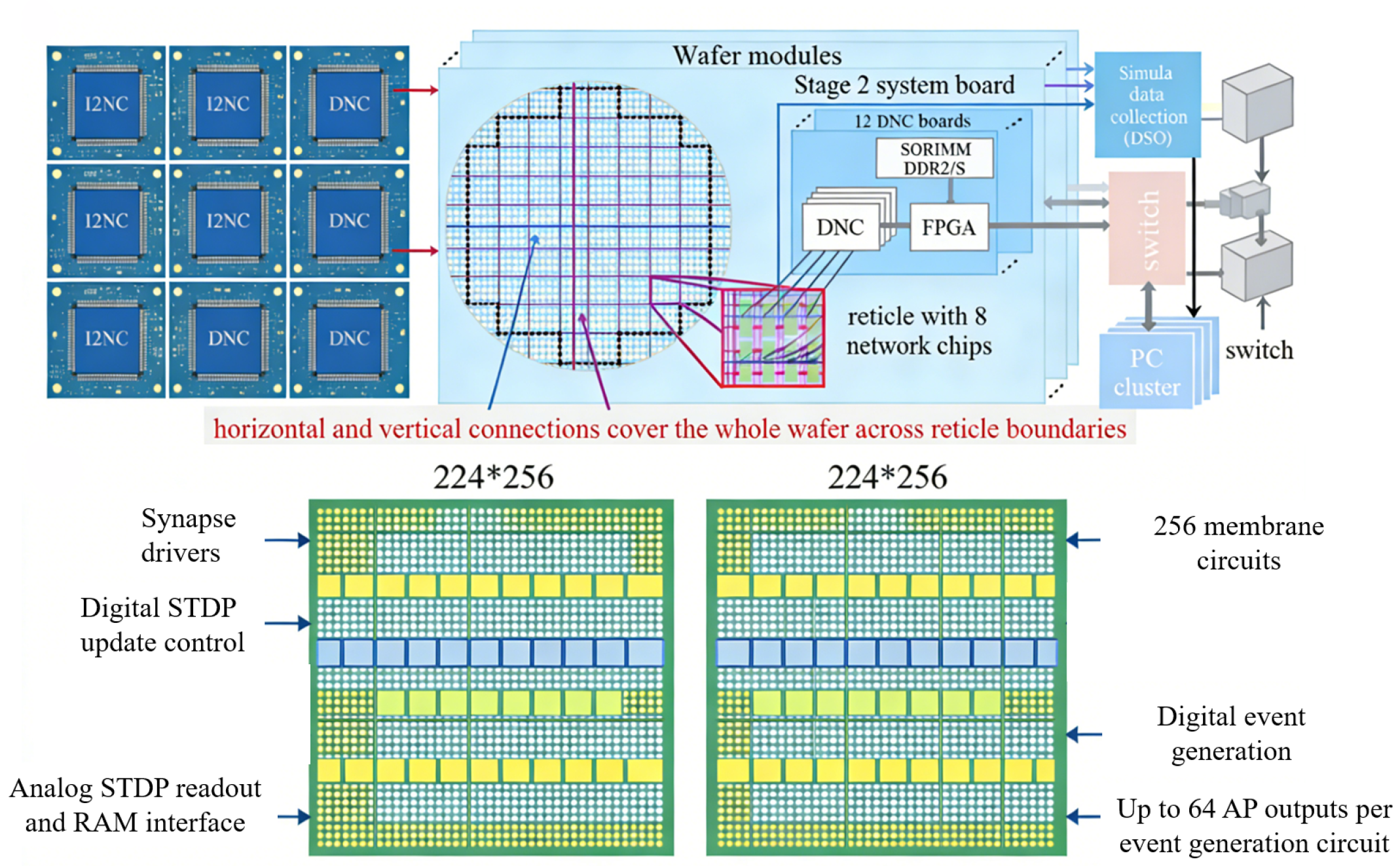
3.1.2. BrainScaleS

BrainScaleS adopts a wafer-scale mixed-signal approach in 65 nm technology, combining accelerated analog neuron dynamics with digital communication infrastructure [27] (see Figure 5). It simulates 196,608 neurons with 50 million synaptic connections while consuming 5.6 W. The system supports STDP plasticity, but its wafer-scale integration introduces manufacturing complexity, positioning it primarily for accelerated neural dynamics research.
BrainScaleS employs mixed-signal CMOS technology to implement neuromorphic components. Neurons utilize subthreshold analog circuits modeling simplified Hodgkin–Huxley dynamics, integrating membrane capacitors, transconductance amplifiers, and spike comparators operating at <0.5 V [28]. Synapses feature programmable current-mirror arrays with 4–8 bit SRAM-stored weights, implementing excitatory/inhibitory pathways through differential pairs while supporting synaptic plasticity mechanisms.
The hierarchical architecture organizes 512-neuron cores with a neuron layer that contains local membrane potential integration circuits, a synaptic crossbar that includes SRAM-weighted connections with time-multiplexed drivers serving multiple virtual neurons [29], and on-chip learning engines that consist of digital processors implementing surrogate gradient algorithms for in situ plasticity.
A hybrid routing scheme enables connectivity with intra-core and inter-core. Intra-core refers to analog current-mode buses with capacitive coupling. As for inter-core, it means that hierarchical AER protocol encoding spikes into 11-bit digital packets. Virtual connectivity achieves full-network communication with 0.1% physical wiring.
The energy efficiency results from (a) domain-specialized processing show analog subthreshold operation and event-driven digital routing, and from (b) optimization techniques show 1000× accelerated real-time simulation, sparse activity exploitation, on-chip learning compensation, and sub-100 μ m synapse-neuron distances [30]. Peak power consumption is constrained to 5.6 W for 200k-neuron systems.
BrainScaleS adopts the Izhikevich model to simulate the firing behavior of neurons, which accurately represents different types of neurons. This model is widely used in neuromorphic computing chips as it efficiently computes neuron spike firing and simulates dynamic neuron behavior. Furthermore, BrainScaleS also supports the STDP rule [31], which simulates synaptic plasticity and learning processes within neural networks.

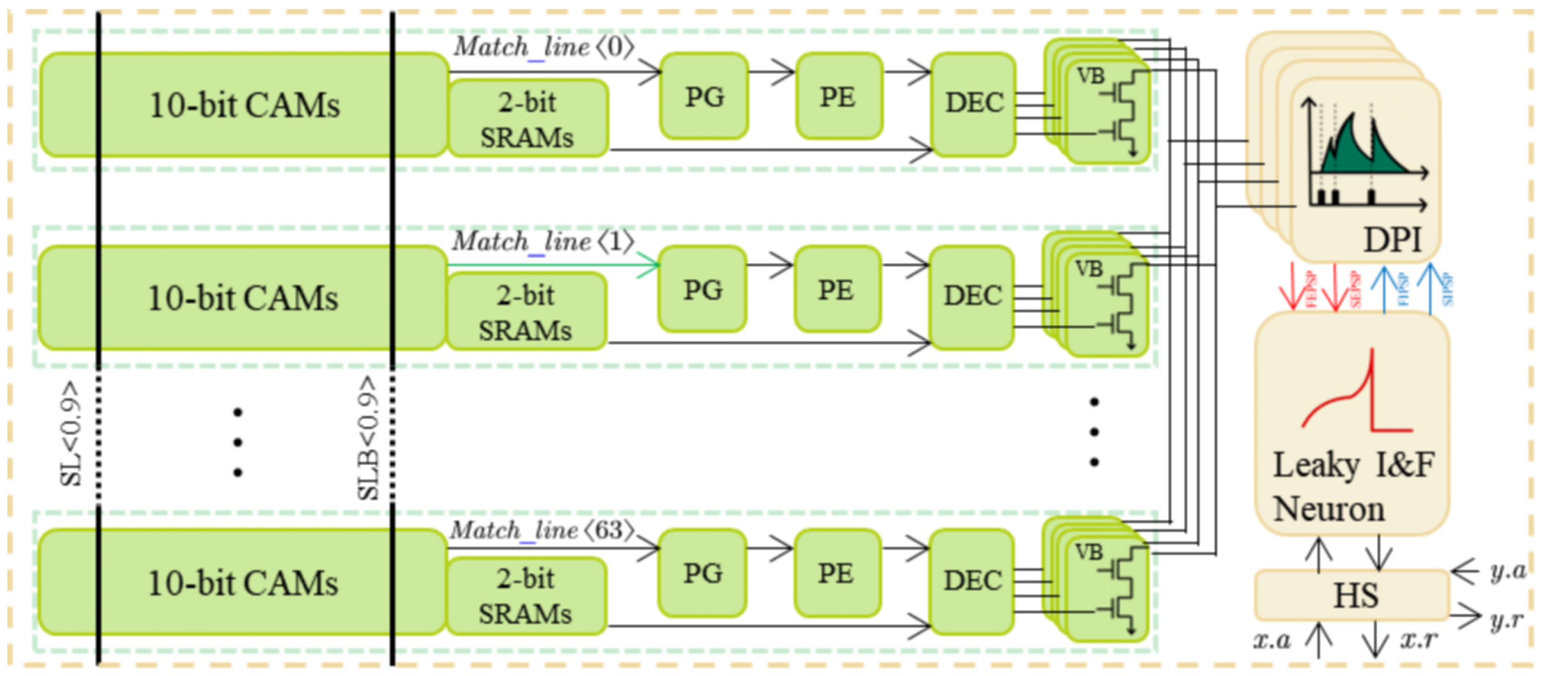
3.1.3. DYNAPs

DYNAPs implements a digital architecture in 180 nm CMOS featuring runtime-reconfigurable synaptic connectivity. It simulates 9216 neurons and 589,824 synapses with well-controlled power consumption [32] (see Figure 6). The design supports both STDP and dynamic network reconfiguration, enabling low-latency event processing ideal for dynamic sensory applications, though with moderate neuron density compared to analog approaches.
DYNAPs utilize mixed-signal circuits. Neurons are typically implemented with analog circuits realizing leaky LIF dynamics, incorporating capacitors for membrane potential integration, comparators for threshold detection, and pulse generators. Synapses employ digital storage for synaptic weights coupled with compact current-steering DACs. Upon receiving a presynaptic spike, the stored weight is converted into an analog current injected into the target neuron’s membrane capacitor.
The core architecture is event-driven and asynchronous for ultra-low power operation. Neuron circuits comprise membrane integrators, leakage circuits, threshold comparators, pulse generators, and circuitry for configurable parameters. Synapse circuits integrate the weight memory with the DAC and pulse response logic. Synaptic dynamics like short-term plasticity can be incorporated within this structure.
Communication between neurons and synapses relies primarily on the AER protocol. When a neuron spikes, its address is encoded and asynchronously placed into an arbitration queue. An arbitrator selects the next event for transmission via a low-swing dedicated digital interconnect fabric [34]. Broadcast address events activate only synapses specifically connected to the spiking neuron, triggering their DAC output to the postsynaptic neuron. This enables efficient, sparse communication.
DYNAPs are organized hierarchically into modular neurocores. Each neurocore contains a local array of neurons, their associated synapses, and dense local interconnect, enabling near-memory computing to minimize data movement energy. Neurocores connect via efficient global AER interconnects. Power reduction stems from multiple strategies: fine-grained power/clock gating down to individual inactive components; event-driven activation; asynchronous control eliminating clock distribution overhead; analog computation for core neural operations; low-swing signaling for communication; and potential 3D integration for high-bandwidth, low-energy vertical connectivity. This combined approach achieves orders-of-magnitude efficiency gains for sparse spiking neural network workloads.
The neuron model used in DYNAPs uses the classical neuron model—the Leaky Integrate-and-Fire model—which is a method that can simulate the action potentials of neurons and the activity with the best efficiency. A threshold excites the neuron’s state and is determined by the accumulation of charge. When the voltage of the neuron is greater than a fixed threshold, it induces a pulse, which then resets the voltage. This is a very good computational model that is able to describe the basic dynamic characteristics of neurons.
Furthermore, DYNAPs are able to learn and adapt in a way that is based on STDP and a sort of synaptic plasticity that modifies synaptic strengths in accordance with temporal relationships of the neurons, as they operate over the same time period as neurons, making DYNAPs effective [18].

3.1.4. ROLLS

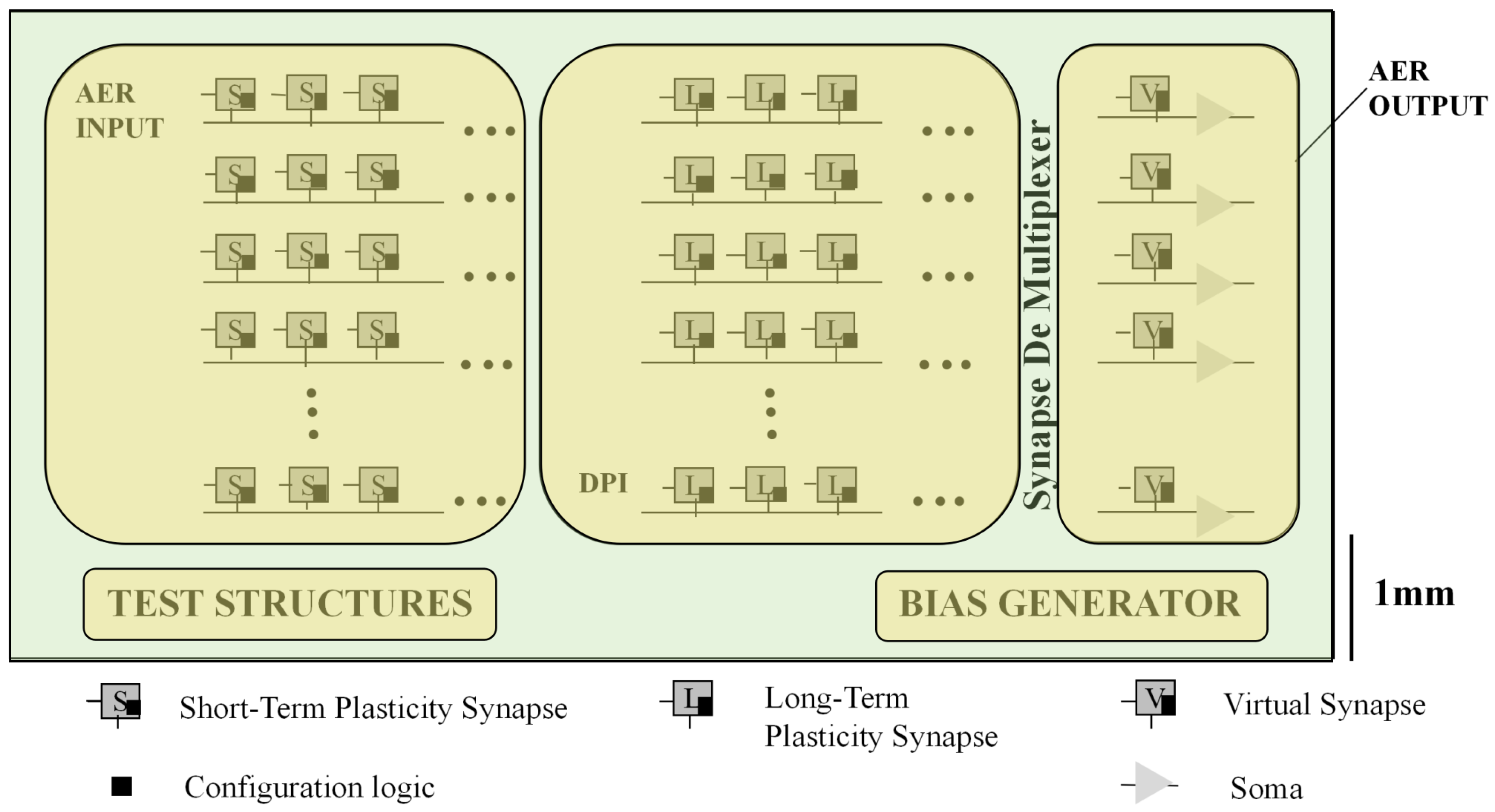
ROLLS combines subthreshold analog neuron circuits with digitally programmable synapses in 180 nm CMOS, achieving ultra-low per-neuron power consumption [35] (see Figure 7). It simulates 256 neurons and 128,000 synapses, implementing multiple plasticity mechanisms within a compact silicon area. However, its severely limited network scale restricts applicability primarily to plasticity mechanism exploration.
In the Institute of Microelectronics of the Chinese Academy of Sciences (IMEC), the Department of Computer and Technology, as well as related organizations, which use sophisticated 180 nm FinFET technology, are working together to create a neuromorphic device known as the ROLLS that was created by the IMEC group [35] (see Figure 7). ROLLS’s chip is capable of simulating 256 neurons and 128,000 synapses, which makes it capable of handling more complex neural network tasks. The ROLLS chip has a low power consumption, which makes it ideal for use in power-sensitive embedded systems or smart terminal applications.
ROLLS utilizes mixed-signal circuits for core neuromorphic elements. Neurons typically implement leaky LIF dynamics via a membrane capacitor integrating input currents, a leak resistor, and a comparator circuit generating output spikes. Synapses combine programmable conductance with local plasticity mechanisms. STDP circuits detect pre- and post-synaptic spike timing differences and adjust synaptic weights accordingly [36]. Crucially, these analog circuits predominantly operate in the subthreshold regime for ultra-low power consumption.
The chip employs a scalable, tile-based architecture. Each computational tile contains a local array of neurons interconnected via a dense, reconfigurable synaptic crossbar. Synaptic cells reside at crosspoints, incorporating weight storage and driver circuitry. Global and local configuration registers enable dynamic tuning of neuronal parameters, synaptic connectivity maps, weight values, and plasticity rules. Dedicated modules manage online learning algorithms and event routing.
Communication within and between tiles relies on the AER protocol. Spiking neurons generate address-coded event packets. A hierarchical or mesh routing network, guided by configuration registers, directs these packets to their target synapses based on decoded addresses [37]. Upon receiving an event, the designated synapse activates, injecting current proportional to its weight into the target neuron’s membrane capacitor. This event-driven, packet-switched paradigm enables the efficient emulation of diverse spiking neural network (SNN) topologies with sparse connectivity.
ROLLS achieves exceptional energy efficiency through synergistic architectural strategies: (a) Pervasive subthreshold analog operation of core neuron/synapse circuits. (b) Strict event-driven activation; inactive components remain in low-power states. (c) Exploitation of sparse activity inherent to SNNs. (d) Asynchronous design, eliminating global clock distribution overhead. (e) Localized memory and processing, minimizing data movement. (f) Fine-grained power gating for unused tiles or circuits. (g) Temporal coding schemes, reducing precision demands on analog circuitry. This organization fundamentally decouples energy consumption from synaptic density, scaling primarily with neural activity.
The neurons model is based on the traditional LIF neuron model, which is a simulation of the dynamic behavior of neurons and when the voltage is above a threshold, the LIF model is based on the accumulation of voltage, and the activation state of each neuron is based upon the accumulation voltage and when the voltage is above a threshold.
A synaptic learning mechanism based on the spontaneous movement of STDP also works by automatically modulating the amount of synaptic weight in light of the pulse’s timing relationship [1]. When working with time data and continuous patterns, this method of learning and memory in biological neural networks is very important to simulate this situation.
Figure 7. ROLLS chip architecture [38].
Chips 05 00003 g007

3.1.5. Comparative Analysis of Digital–Analog Hybrid Chips

The hybrid implementations demonstrate distinct design trade-offs between energy efficiency, scalability, and flexibility. Neurogrid achieves the highest energy efficiency through pure analog implementation, but lacks plasticity support. BrainScaleS offers accelerated computation but with higher complexity and power consumption. DYNAPs provides a good balance between programmability and efficiency, while ROLLS excels in plasticity implementation at the cost of scale.
Neurogrid employs a pure analog architecture implemented in 180 nm CMOS technology, utilizing subthreshold circuits to achieve extreme energy efficiency. This design leverages time-division multiplexing to enable high synaptic density at the expense of plasticity capabilities, making it suitable for real-time brain emulation but limited to static connectivity. BrainScaleS adopts a wafer-scale mixed-signal approach in 65 nm technology, combining accelerated analog neuron dynamics with digital communication infrastructure. While supporting STDP, its wafer-scale integration introduces manufacturing complexity and higher power consumption, positioning it primarily for accelerated neural dynamics research rather than embedded applications.
DYNAPs implements a fully digital architecture using 180 nm CMOS, featuring runtime-reconfigurable synaptic connectivity through programmable routing tables. This design supports both STDP and dynamic network reconfiguration, enabling low-latency event processing ideal for dynamic sensory applications. However, its digital implementation results in moderate neuron density and higher per-neuron energy consumption compared to analog approaches. ROLLS combines subthreshold analog neuron circuits with digitally programmable synapses in 180 nm CMOS, achieving ultra-low per-neuron power consumption through careful operating regime selection. Its distinctive capability lies in implementing multiple plasticity mechanisms within a compact silicon area, though this comes at the cost of severely limited network scale, restricting applicability primarily to plasticity mechanism exploration.
Table 5 compares the digital–analog hybrid chips. With the ongoing progress in chip fabrication techniques, neuromorphic computing chips are anticipated to achieve further advancements in performance and energy efficiency. It is expected that a greater number of neuromorphic chips characterized by low power consumption and high performance will come into existence. These chips are poised to have a significant impact across various domains, including artificial intelligence, deep learning, and biomedical computing. The trend is towards increased integration of chips, enabling them to tackle more intricate computational tasks within a reduced footprint. Concurrently, as hardware learning capabilities continue to enhance, neuromorphic chips will progressively evolve towards adaptive and online learning paradigms, thereby facilitating more efficient real-time intelligent systems.

3.2. Digital-Only Implementation

Neuromorphic computing chips emulate the interaction between neurons and synapses in biological neural systems to execute computational tasks. Unlike traditional computing models, neuromorphic computing emphasizes the efficient handling of parallel computational tasks and provides substantial benefits in terms of energy efficiency. One of the key characteristics of neuromorphic computing chips is their “event-driven” computation model, which means that computation is only triggered based on sensor input or signals, rather than being constantly active like traditional computing systems. This leads to a significant reduction in power consumption.
The core computational models in these chips are typically based on neuron models used in artificial neural networks (e.g., the LIF model, the Izhikevich model) that simulate the transmission process of biological neurons. In addition to differences in computational models, the architecture of neuromorphic chips also varies greatly, primarily in terms of neuron-synapse scale, power management, and on-chip network architecture.

3.2.1. Loihi

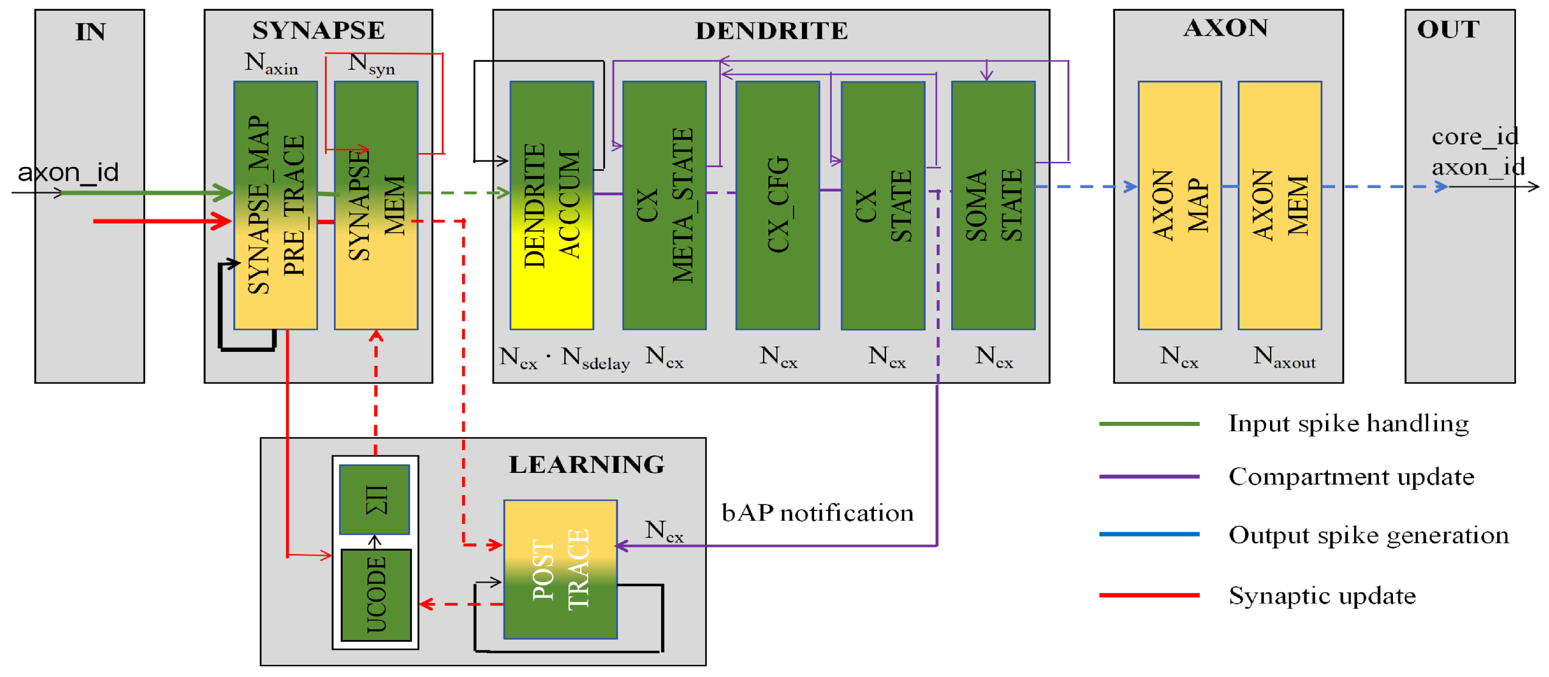
Intel’s Loihi utilizes 14nm process technology to simulate 131,072 neurons and 130 million synapses with 26 W power consumption [39]. The chip employs a hierarchical architecture of asynchronous neurosynaptic cores interconnected via an on-chip network. Its event-driven, asynchronous design enables significant energy efficiency for sparse, event-based computation, making it suitable for low-power edge computing applications (see Figure 8).
The fundamental computational elements within the Loihi chip, specifically neurons and synapses, are realized using highly customized digital logic circuits. Each neurosynaptic core, housing multiple neurons, functions as an asynchronous, event-driven state machine implementing LIF or variant dynamics [41]. Neuron state variables and synaptic weights reside within dedicated on-core SRAM memory blocks. Synapses are not discrete physical devices but are represented by configurable weighted connections stored in memory. Upon spiking, a source neuron triggers the retrieval of synaptic weights associated with its target neurons, which are then integrated into the targets’ membrane potentials or input currents.
Loihi employs a hierarchical architecture comprising numerous independent, asynchronous neurosynaptic cores interconnected via an on-chip network. Each core integrates several key components: (a) A neuron processing unit executing state updates using event-triggered asynchronous logic [18]. (b) Local SRAM storing neuron parameters and incoming/outgoing synaptic weights. (c) A configurable routing table defining the connectivity map for spikes generated locally. (d) An optional dedicated learning engine supporting rules like STDP for online weight adaptation [42]. Core-internal communication utilizes crossbars for efficient event routing.
Functional spiking neural networks are formed through programmable connectivity managed by the routing tables and a packet-switched mesh Network-on-Chip (NoC). When a neuron fires, the local core’s routing table identifies all target destinations. A small packet encapsulating the target address is generated and injected into the asynchronous NoC [43]. Routers within the NoC relay this packet hop-by-hop based on the destination core ID. Upon reaching the target core, the packet is decoded, the relevant synaptic weight is fetched from local memory, and the weighted input is accumulated into the designated target neuron’s state variable. This mechanism enables scalable implementation of sparse, arbitrary network topologies.
Loihi’s significant energy efficiency derives from its event-driven, asynchronous architecture and distributed memory organization. (a) Event-Driven Activation: Components activate predominantly upon spike events, minimizing dynamic power during network inactivity [44]. (b) Asynchronous Design: Elimination of a global clock network removes associated switching power; local handshaking ensures components operate only when necessary. (c) Distributed Memory: Neuron states and synaptic weights are stored in localized SRAM blocks within each core, drastically reducing energy-intensive data movement compared to centralized or off-chip memory. (d) Massive Fine-Grained Parallelism: Numerous cores operate concurrently and independently, distributing computational load efficiently [45]. (e) Efficient On-Chip Communication: The asynchronous NoC transmits only essential spike events, optimizing communication energy. This synergistic organization enables orders-of-magnitude improvements in energy efficiency for sparse, event-based computation. Loihi employs SNN, primarily including the LIF model. Additionally, Loihi supports STDP for synaptic learning rules, simulating the learning and adaptation of neural networks [46].

3.2.2. SpiNNaker

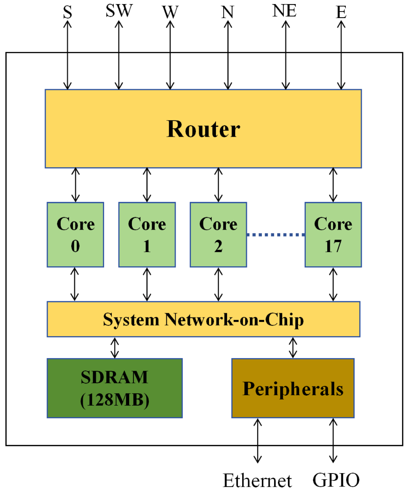
SpiNNaker employs a multicore SoC architecture with ARM processors to simulate large-scale neural networks [47] (see Figure 9). A single chip models 1 billion neurons and 1 trillion synapses with approximately 25 W power consumption. The system utilizes packet-switched communication and globally asynchronous–locally synchronous (GALS) clocking to achieve scalability and power efficiency for massive neural simulations.
SpiNNaker utilizes highly optimized digital ARM processor cores as its fundamental computational units. Each core executes software models to emulate the dynamics of a population of neurons. Synaptic data, including connection weights, target neuron identifiers, and transmission delays, are compactly stored within tightly coupled SRAM memories local to each processor core. These data are organized into efficient lookup structures or connection lists. Neural spike events are triggered by software flags or timer interrupts managed by the core, rather than dedicated analog circuitry.
The chip employs a multicore system-on-chip architecture. A typical SpiNNaker die integrates 18 ARM968 processor cores. Each core possesses dedicated local Instruction and Data Tightly Coupled Memories for fast access to neuron state variables and critical code, and shares access to an off-chip SDRAM controller for larger synaptic parameters [49]. Crucially, a dedicated packet-switched router is integrated adjacent to each core. These routers interconnect via an on-chip NoC. The architecture incorporates globally asynchronous–locally synchronous (GALS) clocking, enabling independent clock domains and supporting power management techniques like clock gating and dynamic voltage and frequency scaling (DVFS).
Intra-chip communication between the 18 cores and their routers occurs through a two-dimensional toroidal mesh NoC. Each router connects directly to its six nearest neighbors. This NoC utilizes a connectionless, packet-based, best-effort routing strategy. Key features include wormhole routing and a minimal packet format. Upon a neural spike event, the originating core generates corresponding packets and injects them into its local router [50]. Routers dynamically compute minimal paths based on the packet’s target address and forward it towards the destination core housing the post-synaptic neurons. This event-driven, asynchronous communication fabric ensures microsecond-scale spike delivery across the chip.
SpiNNaker achieves scalability and ultra-low power consumption through hierarchical modularity. The fundamental module is a single SpiNNaker chip integrating processor cores, routers, and memory. Multiple chips interconnect via high-speed bidirectional asynchronous links on a multi-chip module or node board. Systems scale further by connecting thousands of node boards via inter-rack Ethernet or custom cabling. Power efficiency stems from the following [51]. (a) Event-driven computation: Cores activate only upon receiving spikes or updating active neurons, otherwise entering low-power states via clock gating. (b) Efficient communication: Minimal packet overhead and wormhole routing drastically reduce communication energy. (c) Granular power management: Independent DVFS and clock gating per core/chip region. (d) GALS architecture: Eliminates high power consumption of global clock trees, allowing inactive domains near-zero leakage. This organization enables SpiNNaker to simulate large-scale spiking neural networks with significantly lower power consumption than conventional HPC or GPU clusters.
A neuron simulation model used by SpiNNaker, which is used to process spikes in real-time for each core. This includes updating neuron states, computing synaptic weights, and figuring out spike events [52]. The system simulates neurons that fire according to input spikes by processing events in order to reduce energy consumption.

3.2.3. TrueNorth

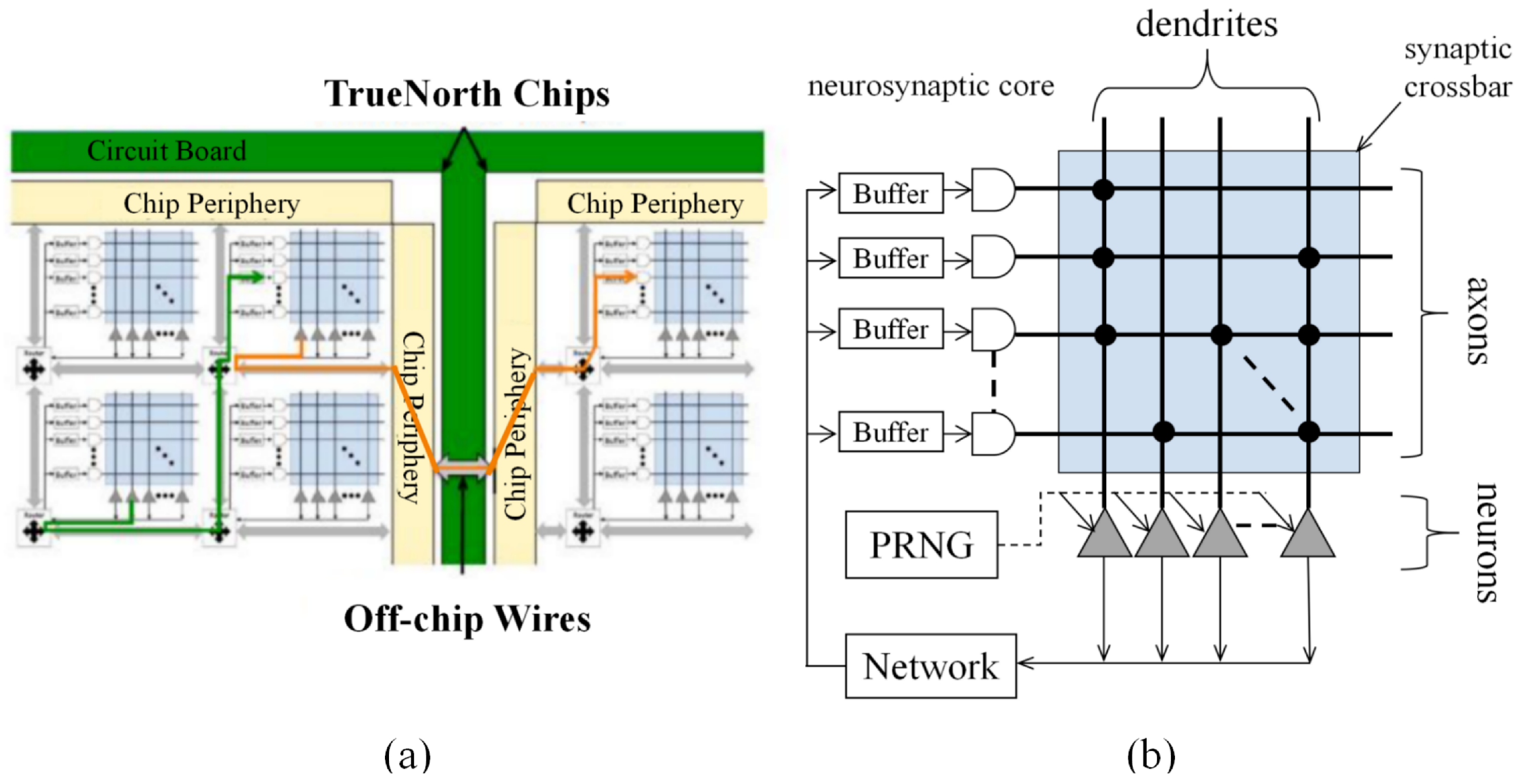
IBM’s TrueNorth implements a digital architecture in 28 nm CMOS, featuring 1 million neurons and 256 million synapses with exceptional power efficiency of 65 mW per million neurons. The chip employs a core-based architecture with event-driven computation and asynchronous operation, eliminating global clock distribution overhead and enabling ultra-low power operation [43] (see Figure 10).
TrueNorth implements neurons and synapses digitally using highly optimized CMOS logic circuits and distributed SRAM blocks. Neurons function as configurable finite-state machines executing LIF dynamics. Their internal state variables are stored in dedicated local registers or SRAM. Synaptic weights are stored as low-precision values within dedicated SRAM arrays physically co-located with their target neurons [43]. This digital approach avoids analog variability and enables precise control while minimizing area and static power.
The fundamental computational module is the neurosynaptic core. Each core integrates several key components: a 256 × 256 configurable synaptic crossbar, 256 individual neuron circuits, dedicated local SRAM for synaptic weights, local event routers, and asynchronous logic controllers. Crucially, computation within the core is event-driven and asynchronous; neurons activate only upon receiving input spikes, eliminating the need for a global clock signal within the core [36,54]. This asynchronous digital design significantly reduces dynamic power consumption.
Communication within and between cores utilizes a hierarchical, packet-switched network. Intra-core routing is handled by the synaptic crossbar, directing input spikes to target neurons. Spikes generated by neurons are queued in local buffers. For inter-core communication, spikes are encoded into small address-event packets. These packets are routed across the chip via a dedicated, energy-efficient 2D mesh NoC. Each core acts as a node in this mesh, containing a simple router that forwards packets based on destination addresses using dimension-ordered routing [55]. This packet-switched, event-based communication minimizes data movement overhead.
The chip is organized as a scalable 2D array of identical neurosynaptic cores. This massive parallelism, combined with three key architectural principles, enables ultra-low power operation. (a) Event-Driven Computation: Neurons remain inactive until triggered by an input event, activating only necessary circuitry. (b) Asynchronous Operation: The absence of a global clock eliminates clock distribution power and enables fine-grained power gating. (c) In-Memory Computation & Sparse Communication: Synaptic weights reside in SRAM adjacent to neuron logic, minimizing data fetch energy. Communication leverages sparse, address-encoded events transmitted only when neurons fire, drastically reducing interconnect activity. This combination results in exceptionally low active power per synaptic operation and very low static power.
The spiked neural network model of TrueNorth is based on the process of event-driven processing. When the membrane potential of neurons achieves a certain value, the network uses the synaptic plasticity and the algorithm of event-based calculation to simulate the brain-like functions, and then the neurons produce spikes [56,57]. This way of modeling complex neural behavior optimizes energy efficiency.

3.2.4. Tianjic

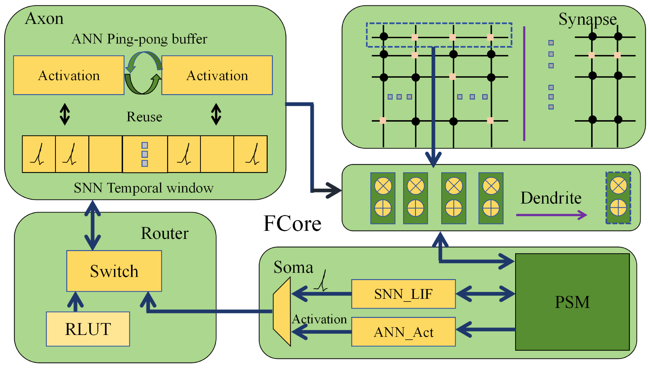
Tianjic, developed by Tsinghua University, uses 28 nm technology to support both spiking and non-spiking neural models on the same chip. It simulates approximately 40,000 spiking neurons and 10 million non-spiking neurons with moderate power consumption [20] (see Figure 11). The heterogeneous many-core architecture enables mapping of diverse neural algorithms onto the same hardware substrate.
The Tianjic chip implements its fundamental computational elements—neurons and synapses—primarily using digital circuitry for flexibility and robustness. Neuron functionality is realized through highly configurable processing units, often structured as finite-state machines or streamlined cores. These units manage state variables and perform operations like integration, leak, and spike generation. Synaptic connections and their associated weights are stored within on-chip memory structures, typically SRAM blocks configured as lookup tables [58]. This digital approach supports the emulation of diverse neural models and synaptic plasticity rules, while also efficiently handling deep learning primitives like vector-matrix multiplication.
The chip employs a heterogeneous many-core architecture composed of numerous replicated Functional Cores. Each FCore integrates several key components: a programmable neuron processing engine, dedicated synaptic weight memory, a routing and scheduling unit for communication management, input/output buffers, and often specialized hardware accelerators for deep learning operations. Crucially, these cores are highly configurable. Parameters such as neuron dynamics, synaptic weight values, inter-core connectivity maps, and the operational mode can be programmed, enabling the mapping of diverse neural algorithms onto the same hardware substrate.
Communication between FCores is orchestrated by a hierarchical event-driven NoC optimized for sparse signal transmission. Within an FCore, local busses or crossbars ensure low-latency interaction between the neuron engine, weight memory, and the scheduler. For core-to-core communication, distributed routers manage the transport of spike events. When a neuron fires, its FCore packages the event into a message. Routers forward these messages based on pre-configured routing tables [40]. Upon arrival at the target FCore, the message is decoded, triggering the retrieval of relevant synaptic weights and the update of the destination neuron’s state. This mechanism efficiently constructs complex functional networks, including feedforward layers, recurrent connections, and convolutional structures, across physically distributed cores.
The organization of Tianjic modules delivers significant power efficiency through several key strategies: massive parallelism enables high throughput at lower clock frequencies; exploitation of sparsity via event-driven computation ensures activity only occurs when necessary; tightly coupled memory-compute integration minimizes energy-intensive data movement by keeping synaptic weights in local SRAM near processing units; and aggressive power management techniques, such as fine-grained clock gating and power gating, dynamically deactivate idle sub-circuits. Collectively, this organization leverages the inherent sparsity of neural computation, particularly in SNN workloads, to achieve substantially lower power consumption compared to conventional architectures performing equivalent tasks.
Tianjic supports traditional artificial neural networks and spiking neural networks on the same chip. It uses mixed-signal computing to simulate both types of neurons [32], and its design makes it highly flexible for various neuromorphic tasks.

3.2.5. PAICORE

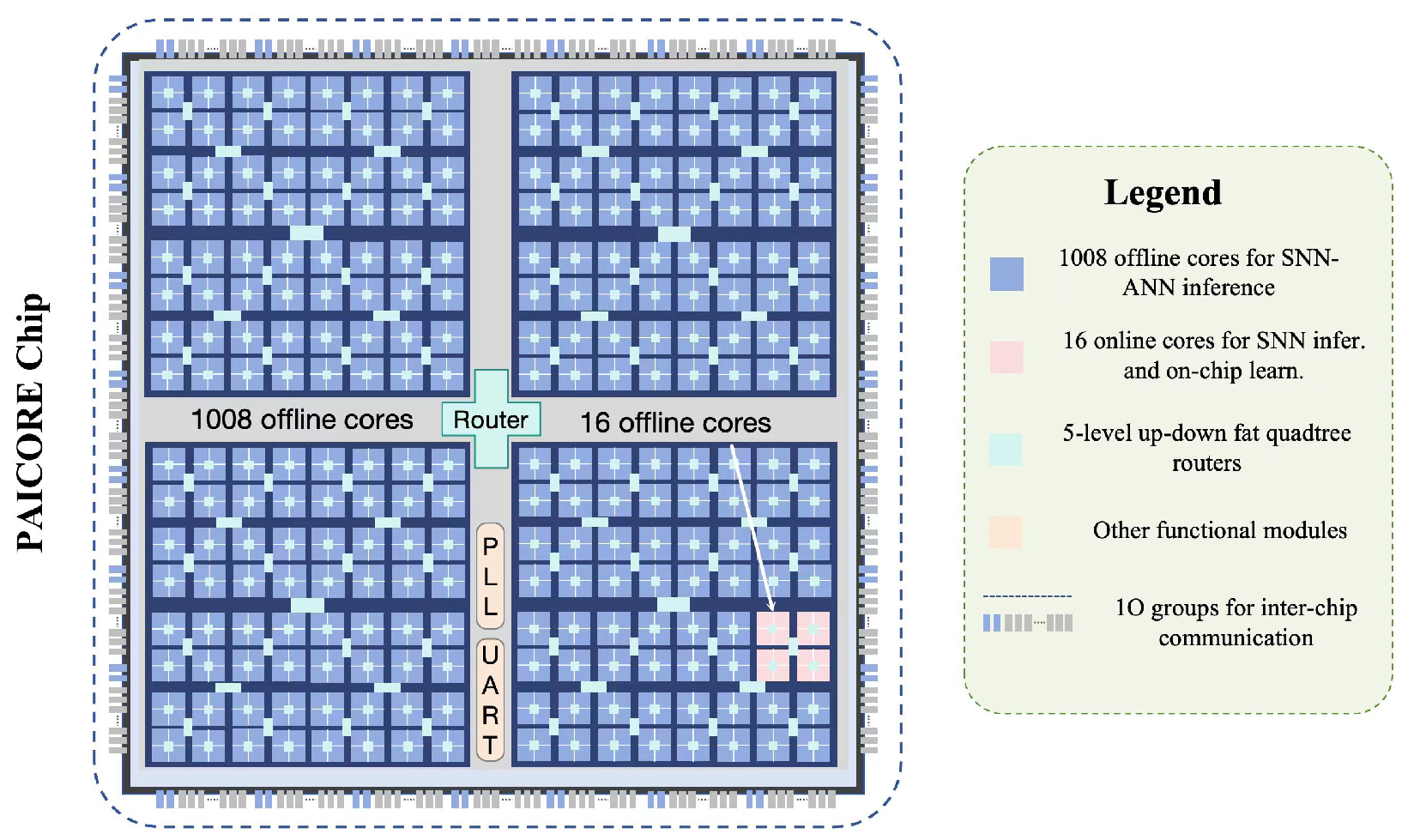
PAICORE integrates digital and analog circuits to support both SNNs and traditional ANNs. The architecture features 156,250 neurons and 156 million synapses with moderate power consumption that adapts based on configuration (see Figure 12). Its design incorporates parallel convolutional units and parameterized spiking neuron arrays optimized for visual processing tasks [58].
The PAICORE chip employs digital circuits to realize LIF neuron models. Neurons integrate incoming spike signals into a membrane potential register; upon exceeding a threshold, they generate an output spike and reset. Synapses function as configurable weighting units, typically implemented via crossbar memory structures for weight storage and dynamic adjustment. This separation enables real-time neuronal computation and reconfigurable synaptic plasticity.
A modular architecture integrates three key components: (a) parallel convolutional units for spatial feature extraction, (b) parameterized spiking neuron arrays supporting configurable thresholds and leak rates, and (c) bit-width-balanced data, which buffers optimizing throughput. These modules interconnect through an event-driven pipeline, activating computations only upon valid data arrival. This design eliminates idle power consumption while accelerating tasks like frame encoding in visual processing.
Intra-chip communication utilizes 64-bit custom data frames governed by a four-phase handshake protocol. Global control signals synchronize multicore operations and system-wide resets [59]. The hybrid interconnection scheme ensures reliable local data transfer while maintaining global state coherence, circumventing bus congestion limitations.
Power efficiency is achieved through three synergistic strategies. (a) Event-Driven Sparsity: Exploiting the temporal sparsity of SNNs, where only active neurons consume dynamic power during spike event. (b) Near-Threshold Voltage Operation: Reducing supply voltage near transistor threshold levels while ensuring reliability. (c) Three-Dimensional Heterogeneous Integration: Vertically stacking neuron and synapse layers using through-silicon vias to minimize interconnect capacitance and delay. These approaches collectively enable significant energy reduction while maintaining computational throughput, with hardware acceleration units offloading software tasks to further enhance efficiency.
PAICORE is capable of supporting both spiking neural networks and traditional artificial neural networks on the same chip. It employs mixed-signal computing to simulate both types of neurons, making its design highly adaptable for a wide variety of neuromorphic tasks.

3.2.6. ODIN

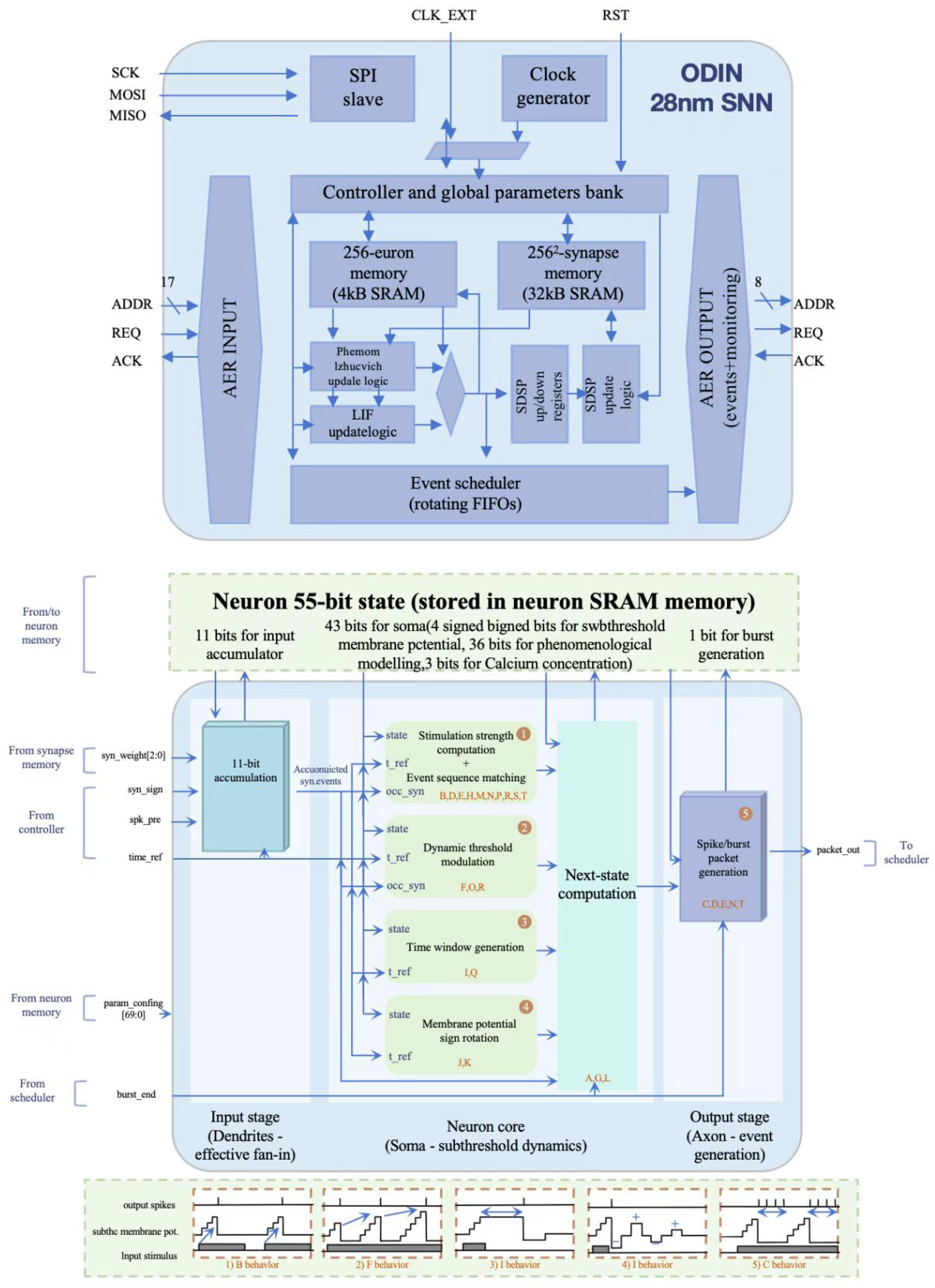
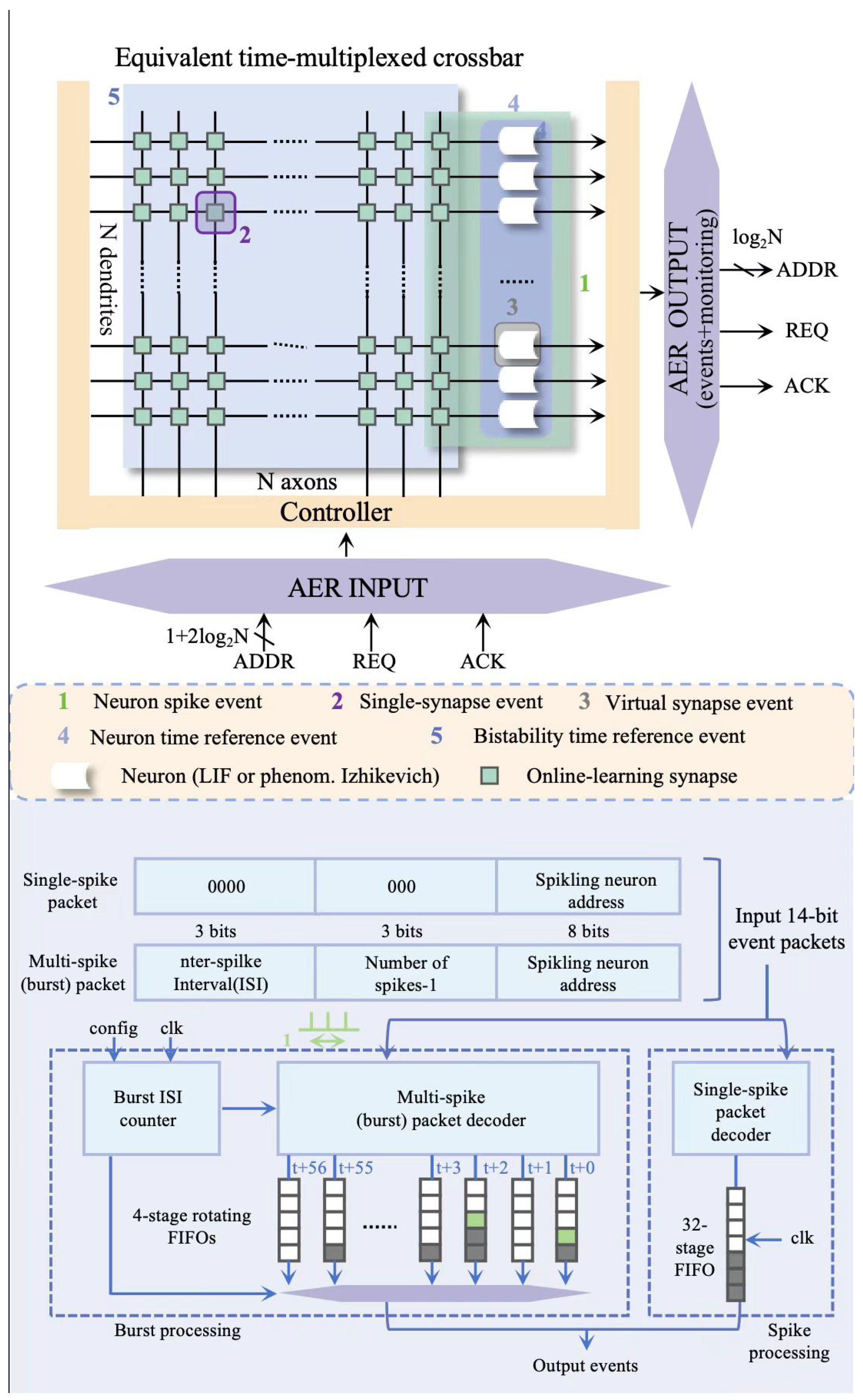
The ODIN chip utilizes 28 nm technology to support 256 neurons and 264,000 synaptic connections with low power consumption. It employs mixed-signal circuits with RRAM-based synaptic arrays [60] (see Figure 13 and Figure 14), implementing a dense crossbar architecture that enables in-memory computation for energy-efficient SNN simulation.
ODIN employs mixed-signal circuits for core neuromorphic components. Neurons utilize analog integrate-and-fire circuits centered on a membrane capacitor for charge accumulation, a comparator for threshold detection, and a reset mechanism. Synapses are implemented using resistive random-access memory (RRAM) devices, typically configured in a 1T1R structure [63]. The transistor facilitates selection and control, while the RRAM’s conductance inherently encodes the synaptic weight. Input spikes modulate the voltage across the RRAM, generating a weighted output current injected into the postsynaptic neuron’s integration circuit.
The core computational architecture is a dense crossbar array enabling in-memory computation. Within this array, rows connect to presynaptic neuron outputs; columns connect to postsynaptic neuron integrators; crosspoints house the 1T1R synaptic units. When a presynaptic neuron fires, its row activates, applying a voltage pulse to connected synapses. The resulting currents, scaled by each RRAM’s conductance, sum vertically along columns [64]. This directly performs the multiply–accumulate operation fundamental to neural networks within the crossbar, eliminating energy-intensive data movement between separate memory and processing units.
Component interconnection relies on hierarchical modularity. The fundamental computational unit is a tile, comprising a local RRAM crossbar array for dense synaptic connectivity, peripheral analog integrate-and-fire neuron circuits, and digital control logic for spike generation and routing. Tiles interconnect via a low-power, event-driven NoC [49]. Spikes are encoded as AER packets and routed asynchronously only upon neuronal activation. This NoC delivers events to destination tiles, where local logic decodes addresses, activates relevant crossbar rows, and updates target neuron states via analog current summation.
ODIN achieves ultra-low power through synergistic device-circuit-architecture co-design, on device or circuit level, RRAM non-volatility eliminates static power. Neurons/subthreshold analog circuits operate with minimal current. Event-driven dynamics ensure idle components draw near-zero power. On an architectural level, crossbar-based in-memory computation removes von Neumann bottleneck energy costs. Sparse, event-triggered communication drastically reduces activity. Tile-level fine-grained power gating deactivates unused modules. Asynchronous design avoids clock distribution overhead. As for the system level, modular tiling confines dense local computation within energy-efficient analog crossbars while minimizing global digital communication via the sparse AER-based NoC. Algorithmic sparsity in SNNs naturally translates to minimal synaptic and neuronal activation. A SNN model is used by ODIN [65]. Through the use of event-driven calculation, this model replicates the activity of neurons and synapses, which allows it to perform complicated neuromorphic tasks well.

3.2.7. Comparative Analysis of Digital-Only Chips

Digital implementations show diverse approaches to balancing scale, efficiency, and functionality. SpiNNaker achieves unprecedented scale through general-purpose processors, while TrueNorth optimizes for extreme power efficiency through specialized event-driven architecture. Loihi provides a balance between scale and learning capability, while Tianjic and PAICORE offer flexibility through support for multiple neural models.
Table 6 compares the digital-only chips. With the development of purely digital realization of the nervous system, their application is also increasingly extensive. There are four main aspects of the development trend.
  • Computational power improvement: As chip fabrication processes continue to improve, neuromorphic chips will be able to support larger-scale neural networks and enhance computational power.
  • Energy efficiency optimization: Low power consumption will remain a design focus, and future chips will achieve a better balance between power consumption and computational power.
  • Model flexibility: Support for hybrid computational models (e.g., SNN, ANN, reinforcement learning, etc.) will become an important direction in future chip design to handle more complex and dynamic tasks.
  • Adaptive learning capability: Future neuromorphic chips will continue to develop adaptive learning functions, enabling real-time optimization based on changing environments.

3.2.8. Recent Advances: Loihi 2 and SpiNNaker 2

Loihi 2 represents Intel’s second-generation neuromorphic research chip, building upon the event-driven asynchronous architecture of its predecessor while introducing significant enhancements. Fabricated in Intel 4 process technology, Loihi 2 features improved neuron models, enhanced programmability, and more efficient inter-chip communication. Key advancements include support for generalized neural models, expanded dendritic compartments, and a more flexible on-chip learning engine that enables a wider range of adaptive algorithms. The chip also introduces improved support for deep learning primitives, bridging the gap between traditional ANNs and SNNs.
SpiNNaker 2, developed through the European Human Brain Project, offers substantial improvements over the original architecture. Each chip integrates 144 ARM M-class processors optimized for simulating spiking neurons, significantly increasing computational density and energy efficiency. Enhanced memory hierarchy and communication infrastructure enable more complex synaptic plasticity rules and larger-scale neural simulations. The system incorporates advanced power management techniques and real-time capabilities, making it suitable for both neuroscience research and robotics applications. SpiNNaker 2’s architecture is particularly tailored for whole-brain simulation projects and closed-loop robotic systems requiring real-time interaction with environments.

3.3. Memristor Implementation

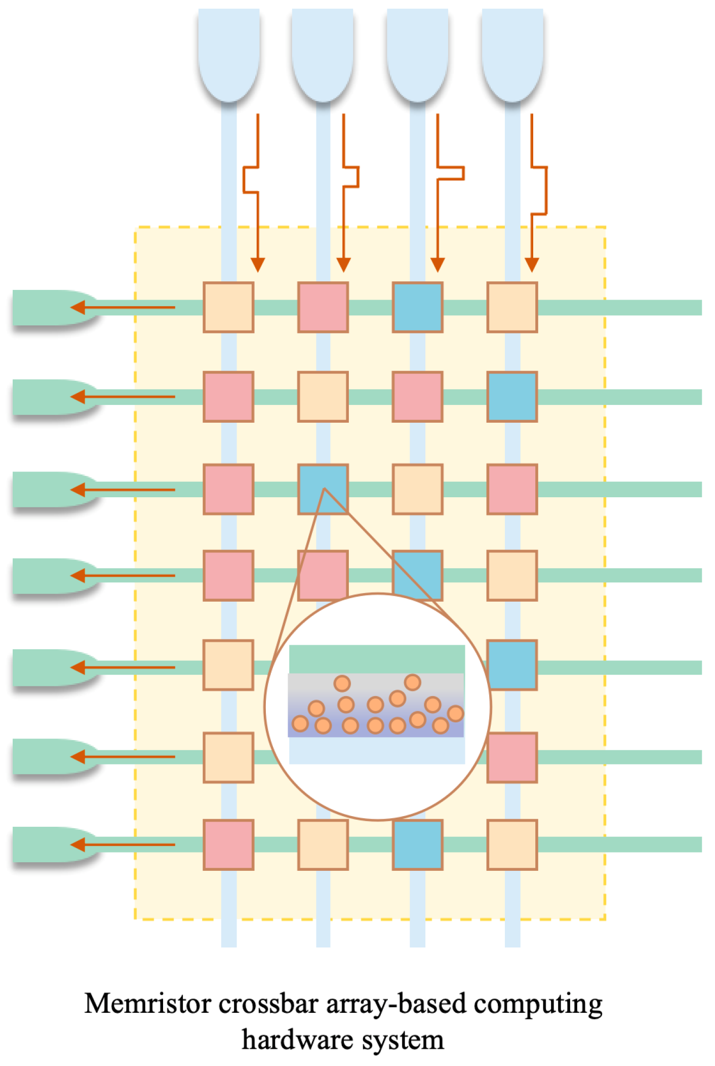
Memristor-based neuromorphic computing leverages the inherent synaptic-like properties of memristive devices to implement efficient in-memory computing architectures. These approaches offer potential for high density and energy efficiency by co-locating memory and computation.

3.3.1. WOx-Based Memristor

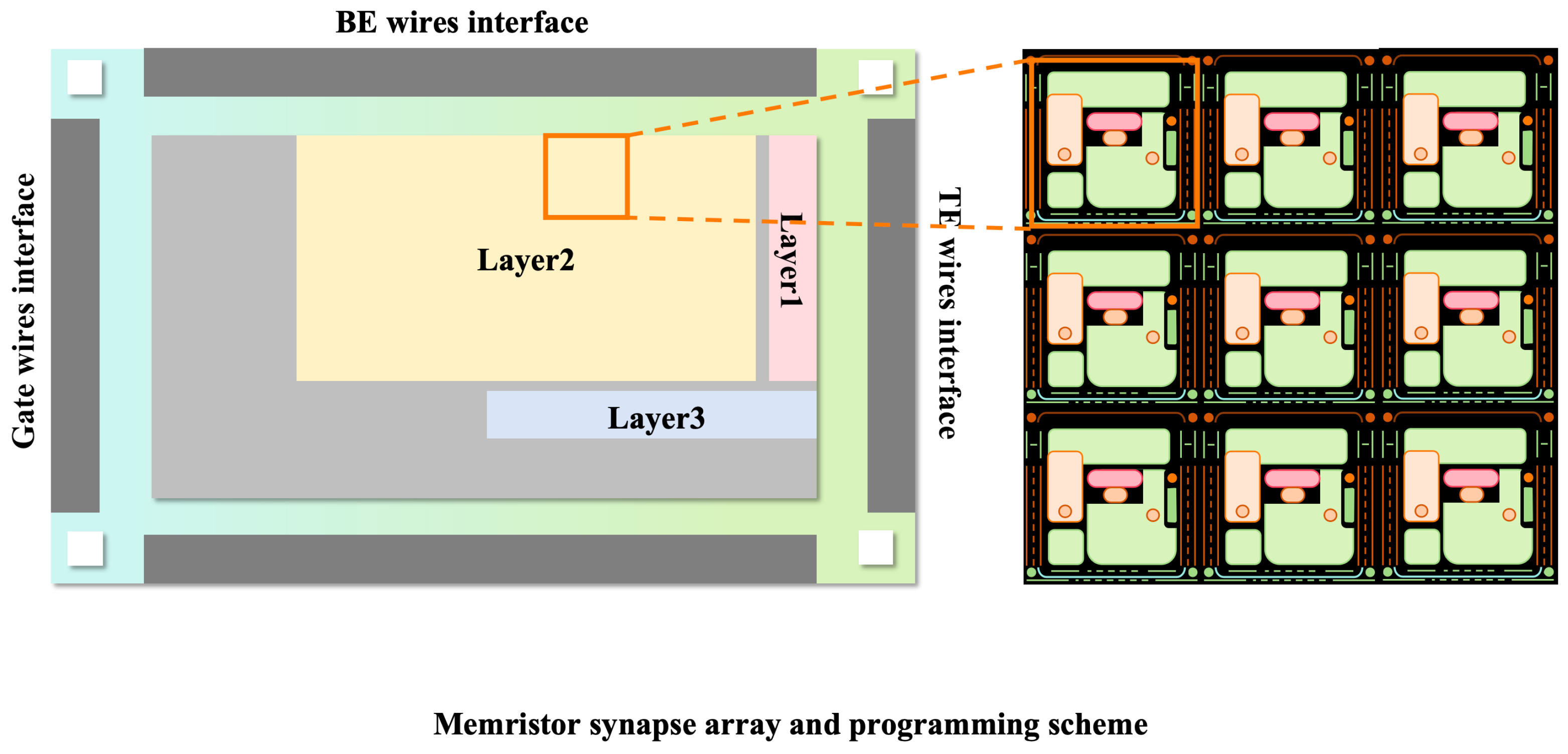
Memristor-based neuromorphic computing leverages the inherent synaptic-like properties of memristive devices to implement efficient in-memory computing architectures. The process and design of this neuromorphic system utilize a 32 × 32 crossbar array of WOx-based analog memristors fabricated via electron-beam lithography, enabling efficient analog vector-matrix multiplication and dynamic reconfigurability for sparse coding tasks. In terms of neurons and synapses, the network emulates biological neurons through leaky integrate-and-fire (LIF) dynamics and synaptic plasticity via memristive conductance modulation, supporting lateral inhibition for sparse feature extraction without physical inhibitory connections. The power consumption is optimized by leveraging memristors’ inherent analog computation capabilities, significantly reducing energy overhead compared to digital implementations. The computation model implements the locally competitive algorithm (LCA) for sparse coding, where iterative forward-backward passes in the crossbar minimize reconstruction error while enforcing sparsity through dynamic neuron inhibition and adaptive dictionary learning. This architecture demonstrates robust performance in natural image processing, even with device variations, highlighting its potential for energy-efficient neuromorphic computing (see Figure 15).
The core component is a WOx-based analog memristor array fabricated via e-beam lithography. Each memristor cell, formed at crosspoints between top (Pd/Au) and bottom (W) electrodes with a WOx switching layer, serves as a programmable synaptic weight. Neuron functions are implemented by peripheral CMOS circuits, including LIF dynamics and thresholding modules, while lateral inhibition is achieved algorithmically without physical inhibitory connections.
The 32 × 32 memristor crossbar performs analog vector-matrix multiplication in situ. Inputs are encoded as pulse-width-modulated voltages applied to rows, with column currents summed via Kirchhoff’s law. Sparse coding is implemented via iterative forward and backward passes, eliminating dedicated inhibitory synapses. An FPGA controls peripheral DACs/ADCs for closed-loop optimization. Input data are loaded row-wise; column outputs are integrated into neuron membrane potentials. Active neurons trigger sparse codes, while reconstruction uses backward passes to update residuals. This dynamic routing enables “compute-in-memory” by merging storage and processing, minimizing data movement. Three key features reduce power: (1) analog in-memory computing eliminates von Neumann bottlenecks; (2) sparse activation limits dynamic power; (3) pulse-width modulation simplifies analog circuits. Non-volatile memristors further cut static power by avoiding refresh cycles.

3.3.2. Pd/HfO2/Ta Memristor

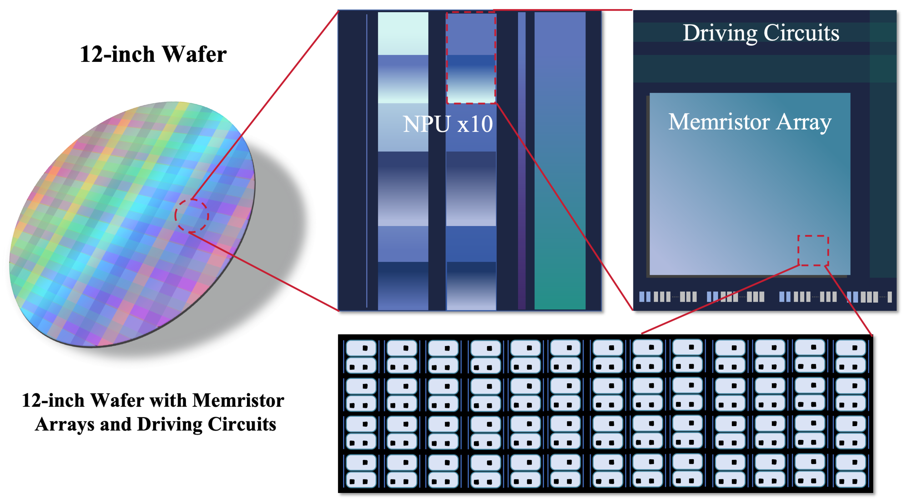
The process and design of this neuromorphic system utilize a 128 × 64 crossbar array of Pd/HfO2/Ta memristors in a one-transistor–one-memristor (1T1R) configuration, manufactured via CMOS-compatible processes with argon plasma treatment and atomic layer deposition (ALD), enabling precise synaptic weight control through transistor-assisted programming. In terms of neuron and synapse, the network implements a three-layer fully connected Q-network with differential memristor pairs for signed weight representation, while neuron activation functions are processed digitally via peripheral CMOS circuits. The power consumption is optimized by leveraging in-memory analog computing for vector-matrix multiplication, reducing data movement energy, and employing a two-pulse write-without-verification scheme for efficient weight updates. The computation model combines hybrid analog–digital reinforcement learning, where analog memristor crossbars perform parallel forward passes for Q-value estimation, while digital components handle experience replay, Bellman error calculation, and RMSprop-based weight updates. This architecture demonstrates robust performance in control tasks with 4–5 bit weight precision, highlighting its potential for energy-efficient autonomous learning systems (see Figure 16).
The memristor employs a 1T1R structure with Pd/HfO2/Ta material stacks. The 60 nm Pd bottom electrode is fabricated via sputtering and lift-off, while the HfO2 switching layer is deposited by atomic layer deposition (ALD) at 250 °C. The top electrode consists of 50 nm Ta and 20 nm Pd. Transistors are fabricated in a commercial foundry, with argon plasma treatment ensuring low contact resistance. Each 4 × 4 μ m2 memristor integrates with a transistor to form an independently controllable synaptic unit.
The circuit configuration employs a 128 × 64 1T1R crossbar array, where each synaptic unit consists of a Pd/HfO2/Ta memristor gated by a foundry-fabricated transistor for precise conductance tuning. The differential-pair architecture enables the representation of signed weights, with adjacent memristors encoding positive and negative values. During computation, all transistors are fully activated, transforming the array into a resistive network that performs parallel analog vector-matrix multiplication via Ohm’s law and Kirchhoff’s current summation. Peripheral transimpedance amplifiers (TIAs) and ADCs/DACs digitize analog outputs for activation functions, while digital logic handles experience replay and RMSprop-based weight updates. The two-pulse write-without-verification scheme ensures efficient programming with minimal energy overhead. This hybrid analog–digital design eliminates von Neumann bottlenecks by co-locating computation and memory, achieving 10× energy efficiency gains in reinforcement learning tasks.
Input data are loaded row-wise, with column currents processed by TIAs/ADCs to generate membrane potentials. The FPGA implements ReLU activation and residual calculation. During backpropagation, weight updates are performed via RMSprop, leveraging differential memristor pairs to eliminate physical inhibitory circuits. Transistors provide current compliance during programming, ensuring linear conductance modulation.
The low-power design leverages three key innovations to significantly reduce energy consumption: in-memory computing enables analog vector-matrix multiplication via Ohm’s and Kirchhoff’s laws in a single step, eliminating data movement overhead; a two-pulse write-without-verify programming scheme minimizes write energy by avoiding iterative verification cycles; and the inherent nonvolatility of memristors maintains synaptic weights without refresh requirements, resulting in near-zero static power consumption, collectively achieving approximately 10× improvement in energy efficiency compared to conventional digital systems.

3.3.3. HPAC Memristor

The HPAC (high-precision analog computing) memristor employs a novel process and design featuring a circuit architecture and dynamic programming protocol that compensates for device-level errors through sequential subarray programming, enabling arbitrarily high precision with low-precision analog devices. For neuron and synapse emulation, it leverages crossbar arrays to perform vector-matrix multiplication (VMM) in the analog domain, mimicking synaptic weights and neuronal computations efficiently. Power consumption is significantly reduced compared to digital approaches, as analog domain computation minimizes energy-intensive data transfers and peripheral circuitry. Its computation model integrates iterative error compensation and preconditioned conjugate gradient (PCG) algorithms, solving complex PDEs and adaptive filters with software-equivalent precision while maintaining high throughput. This co-design of hardware and algorithms bridges the gap between analog device limitations and high-performance computing demands (see Figure 17).
The memristor array employs a 1T1R cell structure, where each analog memristive element is integrated with an access transistor for reliable programming and readout operations. The implementation combines foundry-manufactured 256 × 256 crossbar arrays with peripheral circuits in a system-on-chip configuration, achieving both high density and precision through advanced fabrication techniques. The core architecture features parallel crossbar subarrays with shared analog-to-digital converters, implementing a novel dynamic error compensation algorithm. This configuration enables iterative programming where subsequent subarrays compensate for errors in preceding ones, eliminating the need for complex digital post-processing while maintaining computational accuracy. The design integrates analog computing cores with digital control through hybrid signal paths, where input voltages drive multiple subarrays simultaneously, and output currents are summed in the analog domain. This network architecture combines programming controllers for dynamic mapping, analog vector-matrix multiplication units, and digital interfaces for algorithm coordination, creating a seamless compute pipeline. Energy efficiency is achieved through three key innovations: in-memory analog computation that exploits physical laws for matrix operations, residual-based programming that minimizes quantization overhead, and hardware reuse strategies that eliminate redundant digital circuitry. The design demonstrates >100× improvement in energy efficiency compared to digital ASICs while staying comparable throughput.

3.3.4. VO2-Based Memristor

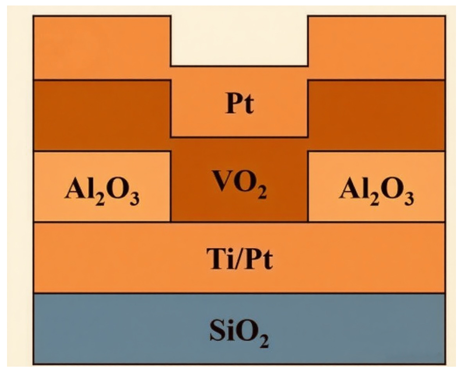
The core of this architecture adopts a 1T1R configuration to build nano-oscillators. The unique insulator-to-metal phase transition property of VO2 enables the device to switch rapidly between high-resistance and low-resistance states when an electric field is applied, which is crucial for simulating the dynamic behavior of neurons (see Figure 18).
In the chip architecture, precise regulation of artificial spin states is achieved through second-harmonic injection locking technology. This regulation mechanism allows the chip to simulate anti-ferromagnetic and ferromagnetic interactions, providing a hardware foundation for parallel computing to solve complex combinatorial optimization problems such as the MAX-CUT problem. In addition, the chip innovatively introduces a real-time error feedback mechanism to realize self-learning capability. When practically applied to video stream processing, the chip can automatically separate moving objects from the background and continuously optimize processing performance as usage time increases. This adaptive learning capability greatly enhances the flexibility and accuracy of the chip in real-time task processing, demonstrating enormous application potential in the field of edge computing.
Oscillators are formed by serially connecting VO2 devices with resistors or CMOS transistors. They are paired with memristor-bridge circuits to enable positive and negative weight regulation, constructing fully connected differential oscillatory neural networks. Some neuron circuits can simulate 23 types of biological neuron dynamics using only two VO2 memristors and passive components.
Anti-phase VO2 pairs form differential neurons, memristor-bridge circuits enable bidirectional weight modulation for excitatory/inhibitory interactions, implementing Hebbian learning via phase-dependent conductance updates, mimicking spike-timing plasticity. Leveraging VO2’s nonlinear dynamics, interconnected modules parallel-process spatiotemporal signals, efficiently emulating pattern recognition and adaptive learning. They achieve low power through their intrinsic metal-insulator transition, triggered by low-voltage biasing ( 68 °C transition temperature) for energy-efficient state switching. Nanoscale thin-film fabrication via PLD or sputtering reduces transition energy.
VO2 memristors stand out with dual-mode switching—non-volatile for long-term memory and volatile for short-term plasticity—enabling versatile neuromorphic emulation [66], as well as self-oscillation via negative differential resistance that can be tuned for frequency generation up to 48 kHz in communication systems [67]. Their simple structure supports high-density integration for compact spiking neural networks, and epitaxially grown VO2 delivers low variability, ensuring consistent performance in precision tasks.

3.3.5. High-Precision 1T1R Memristor

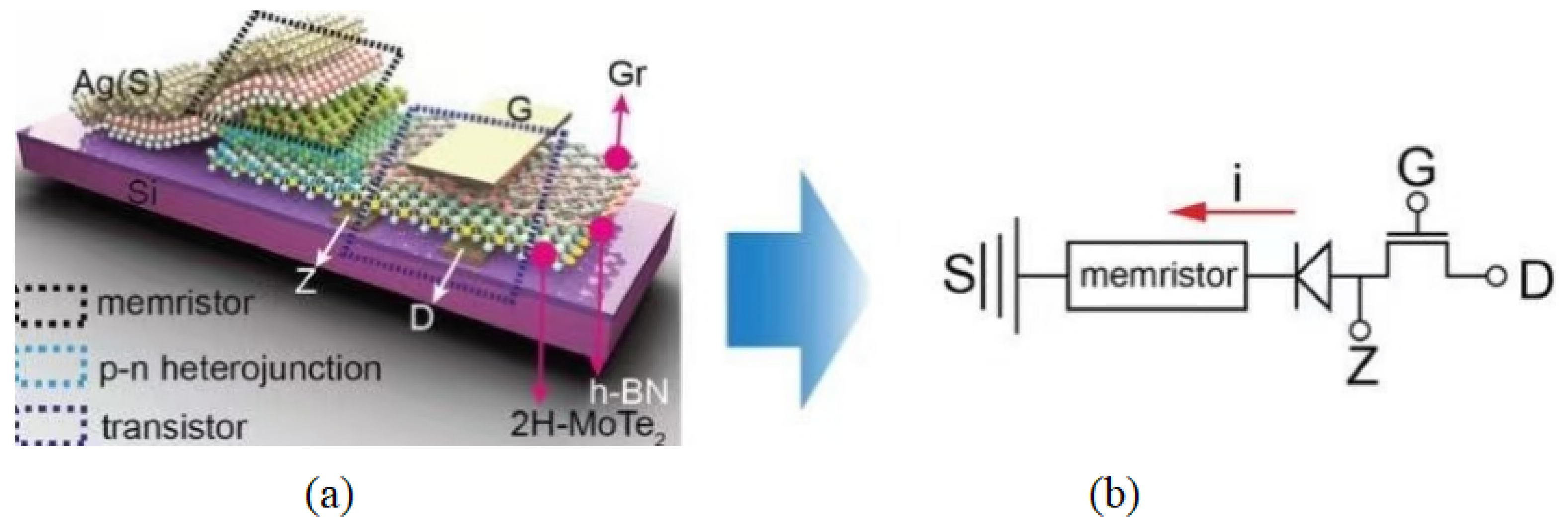
High-precision 1T1R memristors, leveraging metal-oxide materials like HfO2 or Ta2O5, integrate a transistor with a memristor to enable precise conductance control via atomic layer deposition and multi-pulse programming, mitigating variability for sub-1% programming errors. Their crossbar circuit configurations, featuring multi-subarray compensation and dynamic error correction, support high-accuracy analog computing, executing vector-matrix multiplications in O(1) time with DAC/ADC peripherals and FPGA control. Functionally, they integrate into deep neural networks for reinforcement learning and scientific computing (see Figure 19).
High-precision 1T1R array devices use metal-oxide memristors fabricated via atomic layer deposition for precise control of the switching layer thickness. The transistor in each 1T1R unit is integrated via standard foundry processes, enabling conductance tuning within 30–700 mS through gate voltage modulation [68]. Device variability is mitigated via multi-pulse programming to achieve linear, symmetric conductance updates [69].
Figure 19. Schematic diagram of the 1T1R structure [70]. (a) Device architecture of the integrated 1T1R structure. (b) Equivalent electrical circuit of the 1T1R configuration.
Chips 05 00003 g019
High-precision 1T1R arrays employ a 256 × 256 crossbar in which every memristor is gated by a transistor for meticulous conductance control, and they are further augmented with dynamic error-correction circuitry and multi-subarray compensation that push programming error below 1%. The surrounding periphery supplies DACs to generate input voltages, ADCs to sense output currents, and an FPGA backbone that orchestrates real-time weight updates, allowing vector-matrix multiplication to finish in O(1) time [71]. When these arrays are embedded in deep neural networks for reinforcement learning or scientific computing, memristor conductances directly encode synaptic weights and are tuned online via backpropagation; for instance, a cart-pole controller trained with RMSprop achieves 4–5 bit precision per weight. Leveraging multi-subarray integration to cancel device-level errors, the same hardware can solve partial differential equations with high precision while sustaining exceptional energy efficiency [72].
High-precision 1T1R memristors leverage metal-oxide films with efficient oxygen-vacancy migration to minimize switching energy and operate the access transistor in the sub-threshold region to curb standby power. Circuit-level multi-subarray power gating, energy-aware dynamic error correction, and low-voltage DACs/ADCs paired with FPGA control slash data-movement overhead, delivering roughly 10× the energy efficiency of digital ASICs. Each 256 × 256 crossbar cell, scalable to larger arrays, offers 30–700 mS fine-grained conductance tuning with sub-1% programming error—ensuring synaptic-weight accuracy—while its non-volatile retention keeps weights intact without power for persistent edge computing [73]. In-memory matrix-vector multiplication completes in O(1) time, eliminating von Neumann bottlenecks and allowing demanding tasks such as PDE solving.

3.3.6. Comparative Analysis of Memristor Technologies

Recent progress in oxide-based memristor arrays has demonstrated that architectural innovation can be as important as material choice. A representative example is the selector-less TiOx crossbar platform reported by Jeong et al. [74] in Nature Electronics. Although TiOx devices are not a separate memristor category in our taxonomy, their implementation illustrates a significant architectural advance: a forming-free, self-rectifying oxide memristor that enables a one-memristor (1 M) crossbar without additional selector devices. Combined with a hardware-level self-calibration mechanism, this architecture allows reliable analogue MAC operations and real-time video foreground–background separation with accuracy comparable to ideal simulations. These results highlight how oxide-based memristors, when paired with crossbar-level compensation techniques, continue to expand the possibilities for low-power analogue inference (See Table 7).
The WOx memristor crossbar demonstrates distinct advantages through its 32 by 32 analog memristor array architecture, which implements sparse coding algorithms via single-step vector-matrix multiplication enabled by Ohm’s law and Kirchhoff’s current summation, eliminating the need for iterative memory access required in conventional digital systems. This neuromorphic system achieves dynamic sparse optimization through an iterative lateral inhibition mechanism executed via discrete-time forward-backward passes without requiring physical inhibitory synapses, contrasting sharply with static CMOS circuitry implementations. The architecture further differentiates itself through online reprogrammability that supports adaptive feature extraction by modifying dictionary elements from stripe patterns to bar patterns as needed, unlike fixed-function hardware solutions. Experimental validation confirms 4 to 5 bit precision in natural image processing applications while achieving a tenfold improvement in energy efficiency compared to digital systems, collectively demonstrating the superior efficiency and adaptability inherent to this in-memory computing approach.
The 128 × 64 1T1R memristor array demonstrates distinct advantages through its hybrid analog–digital architecture, which implements reinforcement learning via a three-layer deep-Q network physically mapped onto memristor conductances. Unlike conventional von Neumann systems that suffer from data movement bottlenecks between processing units and memory, this design leverages intrinsic physics-based computation, performing vector-matrix multiplication in a single step through Ohm’s law and Kirchhoff’s current summation, thereby achieving O(1) time complexity for multiply–accumulate operations. The differential memristor pairs enable efficient representation of signed weights, while the two-pulse write-without-verification programming scheme ensures 4–5 bit weight precision with minimal energy overhead. Experimental validation on cart-pole and mountain car tasks confirms robust in situ learning capabilities, with potential speed and energy efficiency improvements of nearly an order of magnitude compared to digital platforms, highlighting its promise for autonomous edge computing.
The memristor system-on-chip (SoC) distinguishes itself from traditional in-memory computing architectures by introducing a novel circuit design and programming protocol that achieves arbitrarily high precision using low-precision analog devices. Unlike conventional bit-slicing methods, which rely on predetermined digital states and complex peripheral circuits, this chip employs a dynamic analog approach where subsequent devices compensate for preceding programming errors through weighted summation. This method eliminates the need for extensive digital post-processing, reduces energy consumption, and enhances scalability. Experimental results demonstrate the chip’s capability to solve complex scientific problems, such as partial differential equations, with precision up to 10−15 while maintaining significant power efficiency advantages over digital counterparts. The architecture’s adaptability to device variations and its ability to perform high-precision computations in the analog domain mark a substantial advancement in memristor-based computing.
Recent memristor advances center on unifying material ingenuity, device architecture, and application-driven algorithms. The Ni/WOx/ITO device yields 4-bit analog states with short-term memory, enabling reservoir computing for temporal edge-AI tasks while targeting state stability. Pd/HfO2/Ta stacks provide 24 resistance levels, 1.2 × 10¹¹-cycle endurance, 160 ns/110 ns switching, and 10 10 on/off ratio; monolithic integration with SnS2 transistors in 1T1R arrays accelerates large-scale neuromorphic matrix-vector multiplication. HPAC memristors, though details are sparse, already demonstrate hybrid-chip compatibility and energy-saving potential. VO2-based 1T1R leverages metal–insulator transition for dual-mode non-volatile/volatile operation, low-voltage NDR oscillation, and efficient Ising-machine MAX-CUT solving within wireless IoT nodes. Finally, a 256 × 256 high-precision 1T1R crossbar achieves < 1% programming error and O(1) vector-matrix latency, delivering ten-fold energy savings over ASICs for reinforcement learning and PDE acceleration. Collectively, these platforms chart a roadmap toward higher precision, lower power, and broader deployment in neuromorphic and AI accelerators.

4. Application

Remarkably, neuromorphic computing chips have made significant strides in minimizing power consumption while enhancing performance by mimicking the firing mechanisms of biological neurons. Their applications extend across numerous advanced fields, including artificial systems, adaptive intelligence, neuroscience, and adaptive control systems. By emulating the brain’s neural architecture, neuromorphic computing chips exhibit remarkable adaptability and learning capabilities, positioning them with great potential in these domains. A detailed discussion of their applications in these areas follows below.

4.1. Artificial Intelligence

The continuous advancement in computational power, combined with the swift evolution of deep learning and related technologies, has established artificial intelligence (AI) as one of the most promising and transformative forces in contemporary science and technology. Neuromorphic computing chips, designed to mimic the principles of biological nervous systems, provide robust support for the implementation of AI. The applications of AI technology, particularly in areas such as image recognition and speech processing, have greatly fostered innovation and development across various industries. Figure 20 illustrates a deep learning framework that employs SNNs, showcasing how neuromorphic computing chips can effectively process image data for real-time object detection and classification. These chips excel at simulating the firing patterns, synaptic connections, and learning rules of neurons, highlighting their distinct advantages in executing intelligent tasks, particularly in terms of low power consumption, parallel processing, and real-time responsiveness [34].

4.1.1. Image Recognition

Image recognition is a key application of artificial intelligence, utilized in autonomous driving, security surveillance, and medical imaging analysis. Traditional models, typically based on CNNs, rely on multiple layers for feature extraction but often require significant computing resources, especially with large image datasets. In contrast, neuromorphic computing chips offer advantages by emulating neuronal mechanisms, enabling efficient, low-power processing of image data. These chips can perform real-time feature extraction and classification, showcasing exceptional performance in image recognition and speech processing. For example, Xu et al. [75] propose the hybrid CovDenseSNN framework, which combines the strengths of CNNs and SNNs using unsupervised learning rules, making it well-suited for neuromorphic hardware. In autonomous driving, they analyze camera data in real-time to identify pedestrians, traffic signs, and vehicles, supporting decision-making for autonomous systems [76]. Neuromorphic vision sensors also excel in real-time processing, making them ideal for intelligent monitoring and robotic vision, while improving the flexibility and accuracy of image recognition through the integration of spatial and temporal information. The BrainScaleS system has demonstrated exceptional performance in real-time visual pattern recognition tasks, achieving 10× acceleration compared to conventional hardware. Similarly, Loihi’s event-driven architecture enables efficient processing of dynamic vision sensor data for object tracking applications.

4.1.2. Speech Processing

Speech processing is a key area of artificial intelligence, involving technologies like speech recognition, synthesis, and enhancement. Voice recognition is commonly found in voice assistants, automated customer service, and smart homes. Traditional speech processing models usually rely on long-time feature extraction and speech signal processing [77], which requires high computational cost and processing time.
Neuromorphic computing chips, with their parallel computing capabilities and low-latency features, offer distinct advantages in speech processing tasks. By simulating the firing mechanisms of biological neurons, these chips can efficiently process speech signals, swiftly extract relevant features, and achieve real-time speech recognition. In the context of an intelligent voice assistant, for example, they can promptly identify user commands and respond effectively to voice inputs. The advantages of real-time and low power consumption increase the application of the chips in voice processing [78]. In addition, they can also continuously optimize the speech recognition effect through the adaptive learning mechanism and maintain the high-precision recognition ability under different environmental conditions. Figure 21 shows a neural network-based language model example.
Intel’s Loihi chip has shown remarkable efficiency in speech recognition tasks, processing spoken commands with 5× lower power consumption than traditional DSPs. The SpiNNaker platform has also been successfully deployed for real-time speech separation and enhancement in noisy environments.

4.1.3. Natural Language Processing

Natural language processing (NLP) is a vital technology within the field of artificial intelligence, enabling computers to comprehend, generate, and translate human languages. Traditional NLP models often rely on deep neural networks, such as Transformer architectures, but these models typically demand substantial computing resources and storage. Neuromorphic computing chips, which mimic the brain’s neural network structure, offer a more efficient means of processing natural language data while consuming less power. ERNIE [79], as shown in Figure 22, is a language model trained on a Chinese corpus. It is a knowledge-enhanced semantic representation model with excellent performance in multiple NLP Chinese tasks, language inference, semantic similarity, named entity recognition, and text classification.
In NLP applications, neuromorphic computing chips can maintain efficient and real-time performance when processing text data through efficient neuronal activation and synaptic tuning. For example, machine translation systems can quickly process the conversion information between the source and target languages, thus improving translation accuracy and speed. The parallel computing capabilities of neuromorphic computing chips enable them to handle multiple language tasks simultaneously, thereby enhancing the performance of NLP applications in large-scale data processing and multilingual translation.
TrueNorth’s efficient event-driven architecture has been leveraged for real-time language model inference, particularly for edge applications where power constraints are critical. Recent work has also demonstrated the adaptation of transformer-like architectures to neuromorphic substrates using Loihi 2’s programmable learning rules.

4.1.4. Application Scenario of the Neuromorphic Computing Chips in AI

Neuromorphic computing chips possess a diverse array of applications within artificial intelligence, particularly in areas that demand efficient computing and rapid responses. As AI technology continues to evolve, these chips increasingly showcase their substantial potential in fields such as autonomous driving, intelligent manufacturing, robotics, and smart homes. With their efficient computing power and low power consumption, they serve as an ideal hardware platform for AI applications, especially in edge computing and IoT devices.
In the realm of autonomous driving, these chips facilitate real-time decision-making and precise target detection by rapidly processing sensor data [80]. In smart homes, they enable low-latency responses for voice assistants and smart devices, enhancing the intelligence of home automation systems [81]. In robotics, neuromorphic computing chips empower robots to interact with their environment through sensing and learning, thereby improving their autonomy and adaptability.

4.2. Embodied Intelligence

4.2.1. Perception and Learning

Embodied Intelligence (EI) refers to a robot’s capacity to learn and make decisions through perception and interaction with its environment. In this domain, neuromorphic computing chips emulate the learning mechanisms of biological neurons in dynamic settings, significantly improving the efficiency of robotic perception and decision-making. By processing sensor inputs in real-time, these chips enable robots to swiftly adapt to environmental changes and execute precise action planning and decision-making.
The use of neuromorphic computing chips in the autonomous navigation of robots not only enhances their obstacle-detection capabilities [34], but also enriches their understanding of the environment and adaptive learning by mimicking the synaptic connections found in biological nervous systems [82]. In experiments, robots equipped with these chips can quickly perform path planning in dynamic environments and adjust their behavioral strategies based on real-time feedback.
The DYNAPs architecture has been successfully deployed in robotic navigation systems, enabling real-time environment mapping and obstacle avoidance with power consumption under 100 mW. Figure 23 illustrates the basic architecture of the impulse reinforcement learning algorithm used in these implementations.

4.2.2. Decision-Making and Action Execution

A crucial aspect of machine intelligence is decision-making and action execution. Traditional decision-making algorithms often rely on criterion-based inference or reinforcement learning. In contrast, neuromorphic computing chips offer a more flexible and adaptive approach by emulating the brain’s decision-making processes. For instance, robotic systems utilizing SNNs can dynamically adjust their decision-making strategies in response to environmental changes when tackling complex multi-objective tasks, significantly enhancing their efficiency in executing these tasks.
The low latency and high parallel processing capabilities of neuromorphic computing chips enable the robot to make complex decisions in real-time and swiftly respond to environmental fluctuations. In settings such as smart factories and automated production lines [84], these chips are employed to boost production efficiency and lower energy consumption. Notably, the hybrid Tianjic chip architecture merges the benefits of conventional and neuromorphic computing, greatly enhancing the learning and decision-making capabilities of robots in dynamic environments. This advancement represents a promising technical pathway toward achieving artificial general intelligence (AGI) [20].
Tianjic’s hybrid architecture has demonstrated remarkable performance in autonomous decision-making tasks, enabling real-time adaptation to dynamic environments while maintaining power efficiency. This capability has been particularly valuable in complex multi-objective tasks where traditional control systems struggle with computational complexity.

4.3. Neuroscience

4.3.1. Brain–Computer Interface (BCI)

The integration of neuromorphic computing chips in neuroscience, particularly within the realm of BCI, has emerged as a pivotal factor in advancing neural technology. BCI technology facilitates direct interaction between the human brain and external devices, significantly broadening the potential applications of neuroscience in areas such as medicine, rehabilitation, and intelligent control. Traditional BCI enables real-time communication between the brain and an external controller, as illustrated in Figure 24. It compensates for functional impairments by allowing users to spell words, move a cursor, and control wheelchairs or mechanical arms [85], and neural morphology computing chips, by simulating the activity of neurons, can be closer to the natural behavior of biological systems; thus, in neural signal decoding, they show lower delay and higher energy efficiency.
Intel’s Loihi [40] chip serves as a notable example in the realm of BCI, utilizing SNNs to interpret brain signals and convert them into control commands for external devices. This innovative chip significantly lowers power consumption while enhancing signal processing speed compared to traditional methods. The effective deployment of BCI systems not only advances rehabilitation therapy for patients, such as those suffering from limb paralysis, but also contributes valuable theoretical insights for a new computational paradigm [87]. In the context of facilitating interactions between machines and human thought, the rapid response and adaptability inherent in neuromorphic computing chips have become pivotal for improving decoding accuracy and ensuring real-time performance.
Furthermore, neuromorphic computing chips play an essential role in modeling the dynamics of brain signals. Their ability to process multi-channel electroencephalography (EEG) data in real-time allows researchers to analyze brain activity patterns with greater precision. This functionality is vital for the early diagnosis and ongoing monitoring of neurological conditions like epilepsy [88] and Parkinson’s disease. By deeply analyzing EEG signals, these chips can emulate the brain’s processing mechanisms, yielding accurate data and control algorithms that enhance treatment strategies for neurological disorders.
Intel’s Loihi chip serves as a notable example in the realm of BCI, utilizing SNNs to interpret brain signals and convert them into control commands for external devices. This innovative chip significantly lowers power consumption while enhancing signal processing speed compared to traditional methods.

4.3.2. The Neurodegenerative Diseases Study

In the study of neurodegenerative diseases, neuromorphic computing chips have also demonstrated their great potential [89]. Conditions such as Alzheimer’s and Parkinson’s are frequently associated with the functional degeneration of neurons and the disruption of synaptic connections, presenting considerable challenges to neuroscience research. The efficient parallel processing capabilities of neuromorphic computing chips, along with their ability to accurately simulate neural activity, can aid researchers in developing a deeper understanding of the neural mechanisms underlying these diseases.
For instance, employing neuromorphic computing chips to simulate neural activity in disease states allows researchers to observe the activity patterns of pathological neurons more intuitively. This approach not only enhances the efficiency of neuropathological research but also establishes a theoretical framework for the development of new drugs. By simulating neural signals in pathological states, researchers can identify early-stage biomarkers of the disease, facilitating timely warnings and interventions. The integration of neuromorphic computing chips in neurological disease research has accelerated advancements in precision medicine and personalized treatment.
Compared to traditional computing platforms, neuromorphic computing chips offer distinct advantages in simulating neuronal behavior, processing complex neural activity, and delivering real-time responses, positioning them as valuable tools in neuroscience and medical applications.

4.3.3. Perception–Calculation–Execution Closed Loop

As a groundbreaking technological advancement, neuromorphic systems are increasingly demonstrating their significant potential across various fields, particularly in the integration of sensors and actuators to create adaptive closed-loop systems. This innovative design not only enhances the intelligence of the equipment but also introduces transformative changes across numerous industries. In the case of the tactile prosthesis, the embedded pressure sensors can capture the user’s tactile information in real-time and accurately. This information is then transmitted to the neuromorphic computing chips for efficient encoding. Unlike traditional digital processors, neuromorphic computing chips mimic the way human brain neurons work and can process complex neural signals more quickly and more energy efficiently. The encoded signal is then used to stimulate the neural tissue, thus providing users with delicate tactile feedback. This dynamic feedback mechanism enables the tactile prosthesis to simulate a near-real grasp sensation [90], greatly enhancing the overall user experience.
The ROLLS neuromorphic processor has been successfully integrated into tactile prosthetic systems, providing real-time sensory feedback with minimal latency and power consumption. This implementation demonstrates the unique value of neuromorphic computing in closed-loop biomedical applications.

4.4. Adaptive Control Systems

Adaptive control systems are designed to modify their control strategies in response to changes in their environment. These systems find applications in various fields, including autonomous driving, smart homes, and energy management. Unlike traditional control systems, which rely on fixed control rules and struggle to adapt to dynamic environments, adaptive control systems can dynamically adjust their parameters based on real-time feedback. This capability enables them to effectively respond to variations in both external conditions and internal system states.
Neuromorphic computing chips offer distinct advantages for adaptive control systems due to their capacity for parallel processing and efficient responsiveness, particularly in complex, nonlinear, and variable environments. For instance, DYNAP’s neuromorphic processors are engineered for low-power, large-scale neural network computational tasks, making them well-suited for applications like edge computing, embedded systems, and real-time processing. Their low power consumption and high performance allow DYNAPs to be utilized in a range of smart devices, including smart sensors, autonomous driving systems, and IoT devices. Similarly, the ROLLS neuromorphic processor is primarily employed in edge computing, smart terminals, and IoT devices, benefiting from its low power requirements and high performance in scenarios demanding rapid processing and swift responses.

4.4.1. Autonomous Driving Technology

Autonomous driving technology is an important application field of adaptive control systems. Driverless vehicles need to sense the environment, make decisions, and adjust their driving strategies in real-time. Neuromorphic computing chips, through efficient neuronal simulation and synaptic learning mechanisms, enable driverless systems to rapidly process data from sensors (e.g., lidar, cameras) and make real-time decisions based on this information [91]. Compared to traditional computing platforms, neuromorphic computing chips significantly enhance computing efficiency and reduce processing latency, making driverless systems more adaptable to complex and dynamic road environments.
Loihi and TrueNorth have both been deployed in autonomous vehicle prototypes for real-time sensor fusion and decision-making. These implementations demonstrate 3–5× improvements in energy efficiency compared to traditional GPU-based solutions while maintaining comparable performance.

4.4.2. Smart Homes

In the field of smart homes, the application of adaptive control systems is mainly reflected in environmental awareness and automatic control. As shown in Figure 25, by integrating sensors and actuators, smart home systems can automatically adjust indoor temperature, lighting, humidity, and other parameters according to user preferences and environmental changes [92]. Neuromorphic computing chips can realize real-time perception and decision-making in these systems, helping the system to respond to user needs more quickly and conduct intelligent control.
For instance, in an intelligent temperature control system, the neuromorphic chips can sense the ambient temperature change in real-time, automatically adjusting the working state of the air conditioning or heating according to the user’s preferences. Furthermore, the low power consumption of these chips makes them particularly advantageous for use in smart home devices, making them well-suited for terminal devices like intelligent lighting and automated curtains.

4.4.3. Energy Management

The application of adaptive control systems in energy management is particularly important, especially in smart grid and energy management systems. Neuromorphic computing chips can efficiently process complex sensor data and adapt energy allocation strategies to real-time energy demand and supply conditions. In a smart grid, they can optimize power load distribution, reduce energy waste, and improve the stability and reliability of the grid. Additionally, the home energy management system saves energy and reduces costs by sensing the changes in energy demand in the home, automatically adjusting the working patterns and operating patterns of electrical equipment [93].
Neuromorphic computing chips have shown significant advantages over traditional computing platforms, particularly in domains that require low power consumption, high levels of parallel processing, and real-time adaptability. Their applications span artificial intelligence, embodied intelligence, neuroscience, and adaptive control systems, underscoring their potential to drive innovation and efficiency. As technology progresses, neuromorphic computing chips are expected to play an increasingly vital role in shaping the future of intelligent systems and their applications. They will play an important role in shaping the future of intelligent systems and applications. The applications of the different areas are listed in Table 8.

5. Challenges

Despite significant advancements in neuromorphic chip architecture and applications, several key challenges remain that hinder the large-scale adoption and implementation of neuromorphic systems in practical scenarios. These challenges span hardware, algorithmic design, scalability, and integration with existing computing frameworks.

5.1. Hardware Limitations

One of the most prominent challenges in neuromorphic computing is the hardware limitations associated with scaling up neuromorphic systems. First, the integration of large-scale neurons and synapses into a compact chip remains a significant challenge. Current neuromorphic chips such as Loihi and SpiNNaker offer substantial improvements in the number of neurons they can simulate, but they still face limitations in terms of energy efficiency, parallel processing capabilities, and the number of synapses that can be integrated. These limitations stem from both physical constraints of chip design, such as power dissipation and heat management, and the complexity of interconnecting a massive number of neurons and synapses efficiently. Additionally, the diversity of neuromorphic chip architectures introduces challenges in standardizing hardware platforms for widespread application. Analog designs, while energy-efficient, suffer from limited scalability and integration complexities, while digital designs may not achieve the same level of energy efficiency. Hybrid approaches attempt to combine the strengths of both, but this often leads to increased design complexity and difficulty in achieving optimal performance across different tasks.

5.2. Algorithmic Challenges

Neuromorphic chips, powered by spiking neural networks (SNNs), offer advantages in terms of parallelism, event-driven computation, and low power consumption. However, SNNs require more complex and biologically plausible learning rules such as spike-timing-dependent plasticity (STDP) or voltage-dependent synaptic plasticity (VDSP). These learning mechanisms are still being refined, and their performance is often inferior to that of traditional deep learning models on conventional hardware. While frameworks like NEST and Brian 2 have been developed for simulating spiking neural networks, they are often limited in terms of scalability, making it difficult to implement large-scale deep learning algorithms on neuromorphic systems, and there is a lack of integrated solutions that allow easy deployment of neuromorphic models on actual hardware.

5.3. Scalability and Integration with Existing Systems

Scalability is a major concern for the widespread adoption of neuromorphic computing. While chips like SpiNNaker, Loihi, and Tianjic have demonstrated the ability to simulate millions of neurons, they still fall short of achieving the scale needed for real-world, complex AI applications. The integration of neuromorphic computing systems with existing computing frameworks is another significant hurdle. Current artificial intelligence systems are built on the von Neumann architecture, where memory and computation are separated, and algorithms are typically optimized for these architectures. Neuromorphic systems, on the other hand, integrate memory and computation, which presents difficulties when trying to interface them with traditional systems. Furthermore, the transition from small-scale research experiments to large-scale industrial applications involves addressing issues related to system stability, error tolerance, and communication between chips. Neuromorphic systems, by their very nature, are less deterministic than von Neumann systems, which introduces additional complexity in ensuring reliable performance across large systems, especially in mission-critical applications such as autonomous driving and healthcare.

6. Conclusions and Future Work

6.1. Conclusions

This review has introduced a comprehensive five-dimensional framework for analyzing neuromorphic computing chips, providing a structured comparison across process technology, scale, power consumption, neuronal models, and architectural features. Our refined taxonomy of hybrid architectures clarifies the distinction between various implementation approaches, while the systematic analysis of perception–computation–action closed-loop systems offers new insights into the application potential of neuromorphic hardware. By presenting the evolution of neuromorphic chip architectures from digital-only to hybrid analog–digital designs, we have highlighted both the challenges and successes in scaling neuromorphic systems to meet the demands of real-world applications.

6.2. Future Work

While neuromorphic computing has demonstrated great potential, several technical challenges remain to be addressed for large-scale deployment. Future work can be directed towards the following key areas:
  • Improved Synaptic Plasticity Models:Although current neuromorphic systems use spike-timing-dependent plasticity (STDP) and voltage-dependent synaptic plasticity (VDSP), more biologically plausible models are needed. Research should focus on synaptic plasticity that better mimics brain functions, such as multi-factor learning rules that integrate both short- and long-term memory processes. This will enable neuromorphic systems to adapt more effectively to dynamic environments and complex tasks, improving their performance in real-world AI applications like robotics and autonomous vehicles.
  • Efficient Cross-Layer Communication: Scalability remains a major issue in neuromorphic computing due to limitations in inter-layer communication and data transfer. Future research should focus on developing high-bandwidth, low-latency communication protocols for large-scale neuromorphic systems, particularly for hybrid analog–digital systems. Integration of advanced interconnect technologies, such as optical or memristor-based communication networks, could reduce bottlenecks and enable seamless scaling across larger networks of neuromorphic chips.
  • Hardware–Software Co-Design: The development of integrated toolchains that span from algorithmic development to hardware deployment will be crucial for wider adoption of neuromorphic computing. Future work should focus on creating more accessible programming models and development environments that abstract the underlying hardware complexity while preserving performance and efficiency benefits.

Author Contributions

Conceptualization, G.C.; methodology, M.X.; software, Y.C.; validation, F.Y.; formal analysis, L.Q.; investigation, G.C.; resources, M.X.; data curation, G.C.; writing—original draft preparation, Y.C.; writing—review and editing, F.Y.; visualization, L.Q. and J.R.; supervision, M.X.; project administration, G.C.; funding acquisition, M.X. and J.R. All authors have read and agreed to the published version of the manuscript.

Funding

Fund of Hunan Province Smart Water Digital Twin Research Center, Hunan Water Resources and Hydropower Survey, Design, Planning and Research Co., Ltd (NO.HHPDI-KFJJ-202505).

Data Availability Statement

No new data were created or analyzed in this study. Data sharing is not applicable to this article.

Conflicts of Interest

Author Guang Chen was employed by the Hunan Water Resources and Hydropower Survey, Design, Planning and Research Co., Ltd. The remaining authors declare that the research was conducted in the absence of any commercial or financial relationships that could be construed as a potential conflict of interest.

References

  1. Kudithipudi, D.; Schuman, C.; Vineyard, C.M.; Pandit, T.; Merkel, C.; Kubendran, R.; Aimone, J.B.; Orchard, G.; Mayr, C.; Benosman, R.; et al. Neuromorphic computing at scale. Nature 2025, 637, 801–812. [Google Scholar] [CrossRef]
  2. Rathi, N.; Chakraborty, I.; Kosta, A.; Sengupta, A.; Ankit, A.; Panda, P.; Roy, K. Exploring neuromorphic computing based on spiking neural networks: Algorithms to hardware. ACM Comput. Surv. 2023, 55, 1–49. [Google Scholar] [CrossRef]
  3. Farmakidis, N.; Dong, B.; Bhaskaran, H. Integrated photonic neuromorphic computing: Opportunities and challenges. Nat. Rev. Electr. Eng. 2024, 1, 358–373. [Google Scholar] [CrossRef]
  4. Wahid, S.A.A.; Asad, A.; Mohammadi, F. A Survey on Neuromorphic Architectures for Running Artificial Intelligence Algorithms. Electronics 2024, 13, 2963. [Google Scholar] [CrossRef]
  5. Davies, M.; Wild, A.; Orchard, G.; Sandamirskaya, Y.; Guerra, G.A.F.; Joshi, P.; Plank, P.; Risbud, S.R. Advancing neuromorphic computing with loihi: A survey of results and outlook. Proc. IEEE 2021, 109, 911–934. [Google Scholar] [CrossRef]
  6. Schuman, C.D.; Potok, T.E.; Patton, R.M.; Birdwell, J.D.; Dean, M.E.; Rose, G.S.; Plank, J.S. A survey of neuromorphic computing and neural networks in hardware. arXiv 2017, arXiv:1705.06963. [Google Scholar] [CrossRef]
  7. Yamins, D.L.; DiCarlo, J.J. Using goal-driven deep learning models to understand sensory cortex. Nat. Neurosci. 2016, 19, 356–365. [Google Scholar] [CrossRef]
  8. Ghosh-Dastidar, S.; Adeli, H. Spiking neural networks. Int. J. Neural Syst. 2009, 19, 295–308. [Google Scholar] [CrossRef]
  9. Lin, C.Y.; Chen, P.H.; Lin, H.H.; Huang, W.M. U (1) dynamics in neuronal activities. Sci. Rep. 2022, 12, 17629. [Google Scholar] [CrossRef]
  10. Zeni, C.; Pinsler, R.; Zügner, D.; Fowler, A.; Horton, M.; Fu, X.; Wang, Z.; Shysheya, A.; Crabbé, J.; Ueda, S.; et al. A generative model for inorganic materials design. Nature 2025, 639, 624–632. [Google Scholar] [CrossRef]
  11. Izhikevich, E.M. Simple model of spiking neurons. IEEE Trans. Neural Netw. 2003, 14, 1569–1572. [Google Scholar] [CrossRef]
  12. Wang, J.; Xu, J.; Mo, X.; Qiu, J. The critical avalanche of an excitation–inhibition neural network composed of Izhikevich neurons is studied based on the bifurcation of the mean-field. Chaos Solitons Fractals 2025, 190, 115772. [Google Scholar] [CrossRef]
  13. Guo, D.; Li, C. Self-sustained irregular activity in 2-D small-world networks of excitatory and inhibitory neurons. IEEE Trans. Neural Netw. 2010, 21, 895–905. [Google Scholar] [PubMed]
  14. Heidarpur, M.; Ahmadi, A.; Ahmadi, M.; Azghadi, M.R. CORDIC-SNN: On-FPGA STDP learning with izhikevich neurons. IEEE Trans. Circuits Syst. Regul. Pap. 2019, 66, 2651–2661. [Google Scholar] [CrossRef]
  15. Xu, Q.; Liu, T.; Ding, S.; Bao, H.; Li, Z.; Chen, B. Extreme multistability and phase synchronization in a heterogeneous bi-neuron Rulkov network with memristive electromagnetic induction. Cogn. Neurodynamics 2023, 17, 755–766. [Google Scholar] [CrossRef] [PubMed]
  16. Wu, Y.; Deng, L.; Li, G.; Zhu, J.; Shi, L. Spatio-temporal backpropagation for training high-performance spiking neural networks. Front. Neurosci. 2018, 12, 331. [Google Scholar]
  17. Bellec, G.; Scherr, F.; Subramoney, A.; Hajek, E.; Salaj, D.; Legenstein, R.; Maass, W. A solution to the learning dilemma for recurrent networks of spiking neurons. Nat. Commun. 2020, 11, 3625. [Google Scholar] [CrossRef]
  18. Yik, J.; Van den Berghe, K.; den Blanken, D.; Bouhadjar, Y.; Fabre, M.; Hueber, P.; Ke, W.; Khoei, M.A.; Kleyko, D.; Pacik-Nelson, N.; et al. The neurobench framework for benchmarking neuromorphic computing algorithms and systems. Nat. Commun. 2025, 16, 1545. [Google Scholar] [CrossRef]
  19. Liu, Z.; Mei, J.; Tang, J.; Xu, M.; Gao, B.; Wang, K.; Ding, S.; Liu, Q.; Qin, Q.; Chen, W.; et al. A memristor-based adaptive neuromorphic decoder for brain–computer interfaces. Nat. Electron. 2025, 8, 362–372. [Google Scholar] [CrossRef]
  20. Pei, J.; Deng, L.; Song, S.; Zhao, M.; Zhang, Y.; Wu, S.; Wang, G.; Zou, Z.; Wu, Z.; He, W.; et al. Towards artificial general intelligence with hybrid Tianjic chip architecture. Nature 2019, 572, 106–111. [Google Scholar] [CrossRef]
  21. Merolla, P.A.; Arthur, J.V.; Alvarez-Icaza, R.; Cassidy, A.S.; Sawada, J.; Akopyan, F.; Jackson, B.L.; Imam, N.; Guo, C.; Nakamura, Y.; et al. A million spiking-neuron integrated circuit with a scalable communication network and interface. Science 2014, 345, 668–673. [Google Scholar] [CrossRef] [PubMed]
  22. Boi, F.; Moraitis, T.; De Feo, V.; Diotalevi, F.; Bartolozzi, C.; Indiveri, G.; Vato, A. A bidirectional brain-machine interface featuring a neuromorphic hardware decoder. Front. Neurosci. 2016, 10, 563. [Google Scholar] [CrossRef] [PubMed]
  23. Benjamin, B.V.; Gao, P.; McQuinn, E.; Choudhary, S.; Chandrasekaran, A.R.; Bussat, J.M.; Alvarez-Icaza, R.; Arthur, J.V.; Merolla, P.A.; Boahen, K. Neurogrid: A mixed-analog-digital multichip system for large-scale neural simulations. Proc. IEEE 2014, 102, 699–716. [Google Scholar]
  24. Billaudelle, S.; Stradmann, Y.; Schreiber, K.; Cramer, B.; Baumbach, A.; Dold, D.; Göltz, J.; Kungl, A.F.; Wunderlich, T.C.; Hartel, A.; et al. Versatile emulation of spiking neural networks on an accelerated neuromorphic substrate. In Proceedings of the 2020 IEEE International Symposium on Circuits and Systems (ISCAS), Seville, Spain, 12–14 October 2020; IEEE: Washington, DC, USA, 2020; pp. 1–5. [Google Scholar]
  25. Khodagholy, D.; Gelinas, J.N.; Thesen, T.; Doyle, W.; Devinsky, O.; Malliaras, G.G.; Buzsáki, G. NeuroGrid: Recording action potentials from the surface of the brain. Nat. Neurosci. 2015, 18, 310–315. [Google Scholar] [CrossRef]
  26. Johnson, M. Mapping the mind: A new tool reveals uncharted territories in the brain. Nat. Med. 2017, 23, 144–147. [Google Scholar] [CrossRef]
  27. Waldrop, M.M. Smart connections. Nature 2013, 503, 22. [Google Scholar] [CrossRef]
  28. Oldroyd, P.; Velasco-Bosom, S.; Bidinger, S.L.; Hasan, T.; Boys, A.J.; Malliaras, G.G. Fabrication of thin-film electrodes and organic electrochemical transistors for neural implants. Nat. Protoc. 2025, 20, 2100–2124. [Google Scholar] [CrossRef]
  29. Hong, G.; Lieber, C.M. Novel electrode technologies for neural recordings. Nat. Rev. Neurosci. 2019, 20, 330–345. [Google Scholar]
  30. Roy, K.; Jaiswal, A.; Panda, P. Towards spike-based machine intelligence with neuromorphic computing. Nature 2019, 575, 607–617. [Google Scholar] [CrossRef]
  31. Zhang, W.; Ma, S.; Ji, X.; Liu, X.; Cong, Y.; Shi, L. The development of general-purpose brain-inspired computing. Nat. Electron. 2024, 7, 954–965. [Google Scholar]
  32. He, W.; Zhu, J.; Feng, Y.; Liang, F.; You, K.; Chai, H.; Sui, Z.; Hao, H.; Li, G.; Zhao, J.; et al. Neuromorphic-enabled video-activated cell sorting. Nat. Commun. 2024, 15, 10792. [Google Scholar] [CrossRef]
  33. Moradi, S.; Qiao, N.; Stefanini, F.; Indiveri, G. A scalable multicore architecture with heterogeneous memory structures for dynamic neuromorphic asynchronous processors (DYNAPs). IEEE Trans. Biomed. Circuits Syst. 2017, 12, 106–122. [Google Scholar] [CrossRef]
  34. Schuman, C.D.; Kulkarni, S.R.; Parsa, M.; Mitchell, J.P.; Date, P.; Kay, B. Opportunities for neuromorphic computing algorithms and applications. Nat. Comput. Sci. 2022, 2, 10–19. [Google Scholar] [CrossRef]
  35. Wu, Y.; Zhao, R.; Zhu, J.; Chen, F.; Xu, M.; Li, G.; Song, S.; Deng, L.; Wang, G.; Zheng, H.; et al. Brain-inspired global-local learning incorporated with neuromorphic computing. Nat. Commun. 2022, 13, 65. [Google Scholar] [CrossRef] [PubMed]
  36. Zhang, Y.; Qu, P.; Ji, Y.; Zhang, W.; Gao, G.; Wang, G.; Song, S.; Li, G.; Chen, W.; Zheng, W.; et al. A system hierarchy for brain-inspired computing. Nature 2020, 586, 378–384. [Google Scholar] [CrossRef] [PubMed]
  37. Van Doremaele, E.; Ji, X.; Rivnay, J.; Van De Burgt, Y. A retrainable neuromorphic biosensor for on-chip learning and classification. Nat. Electron. 2023, 6, 765–770. [Google Scholar] [CrossRef]
  38. Qiao, N.; Mostafa, H.; Corradi, F.; Osswald, M.; Stefanini, F.; Sumislawska, D.; Indiveri, G. A reconfigurable on-line learning spiking neuromorphic processor comprising 256 neurons and 128K synapses. Front. Neurosci. 2015, 9, 141. [Google Scholar] [CrossRef]
  39. Bezugam, S.S.; Shaban, A.; Suri, M. Neuromorphic recurrent spiking neural networks for emg gesture classification and low power implementation on loihi. In Proceedings of the 2023 IEEE International Symposium on Circuits and Systems (ISCAS), Monterey, CA, USA, 21–25 May 2023; IEEE: Washington, DC, USA, 2023; pp. 1–5. [Google Scholar]
  40. Davies, M.; Srinivasa, N.; Lin, T.H.; Chinya, G.; Cao, Y.; Choday, S.H.; Dimou, G.; Joshi, P.; Imam, N.; Jain, S.; et al. Loihi: A neuromorphic manycore processor with on-chip learning. IEEE Micro 2018, 38, 82–99. [Google Scholar] [CrossRef]
  41. Kleyko, D.; Kymn, C.J.; Thomas, A.; Olshausen, B.A.; Sommer, F.T.; Frady, E.P. Principled neuromorphic reservoir computing. Nat. Commun. 2025, 16, 640. [Google Scholar] [CrossRef]
  42. Rao, A.; Plank, P.; Wild, A.; Maass, W. A long short-term memory for AI applications in spike-based neuromorphic hardware. Nat. Mach. Intell. 2022, 4, 467–479. [Google Scholar]
  43. Smith, J.D.; Hill, A.J.; Reeder, L.E.; Franke, B.C.; Lehoucq, R.B.; Parekh, O.; Severa, W.; Aimone, J.B. Neuromorphic scaling advantages for energy-efficient random walk computations. Nat. Electron. 2022, 5, 102–112. [Google Scholar] [CrossRef]
  44. Pedersen, J.E.; Abreu, S.; Jobst, M.; Lenz, G.; Fra, V.; Bauer, F.C.; Muir, D.R.; Zhou, P.; Vogginger, B.; Heckel, K.; et al. Neuromorphic intermediate representation: A unified instruction set for interoperable brain-inspired computing. Nat. Commun. 2024, 15, 8122. [Google Scholar] [CrossRef] [PubMed]
  45. Imam, N.; Cleland, T.A. Rapid online learning and robust recall in a neuromorphic olfactory circuit. Nat. Mach. Intell. 2020, 2, 181–191. [Google Scholar] [CrossRef]
  46. Sandamirskaya, Y.; Kaboli, M.; Conradt, J.; Celikel, T. Neuromorphic computing hardware and neural architectures for robotics. Sci. Robot. 2022, 7, eabl8419. [Google Scholar] [CrossRef] [PubMed]
  47. Kawasetsu, T.; Ishida, R.; Sanada, T.; Okuno, H. A hardware system for emulating the early vision utilizing a silicon retina and SpiNNaker chips. In Proceedings of the 2014 IEEE Biomedical Circuits and Systems Conference (BioCAS) Proceedings, Lausanne, Switzerland, 22–24 October 2014; IEEE: Washington, DC, USA, 2014; pp. 552–555. [Google Scholar]
  48. Furber, S.B.; Galluppi, F.; Temple, S.; Plana, L.A. The spinnaker project. Proc. IEEE 2014, 102, 652–665. [Google Scholar] [CrossRef]
  49. Soto, M.; Serrano-Gotarredona, T.; Linares-Barranco, B. An Intrinsic Method for Fast Parameter Update on the SpiNNaker Platform. In Proceedings of the 2018 IEEE International Symposium on Circuits and Systems (ISCAS), Florence, Italy, 27–30 May 2018; IEEE: Washington, DC, USA, 2018; pp. 1–5. [Google Scholar]
  50. Haessig, G.; Galluppi, F.; Lagorce, X.; Benosman, R. Neuromorphic networks on the SpiNNaker platform. In Proceedings of the 2019 IEEE International Conference on Artificial Intelligence Circuits and Systems (AICAS), Hsinchu, Taiwan, 18–20 March 2019; IEEE: Washington, DC, USA, 2019; pp. 86–91. [Google Scholar]
  51. Schoepe, T.; Janotte, E.; Milde, M.B.; Bertrand, O.J.; Egelhaaf, M.; Chicca, E. Finding the gap: Neuromorphic motion-vision in dense environments. Nat. Commun. 2024, 15, 817. [Google Scholar] [CrossRef]
  52. Lu, W.; Du, X.; Wang, J.; Zeng, L.; Ye, L.; Xiang, S.; Zheng, Q.; Zhang, J.; Xu, N.; Feng, J.; et al. Simulation and assimilation of the digital human brain. Nat. Comput. Sci. 2024, 4, 890–898. [Google Scholar] [CrossRef]
  53. Akopyan, F.; Sawada, J.; Cassidy, A.; Alvarez-Icaza, R.; Arthur, J.; Merolla, P.; Imam, N.; Nakamura, Y.; Datta, P.; Nam, G.J.; et al. TrueNorth: Design and tool flow of a 65 mw 1 million neuron programmable neurosynaptic chip. IEEE Trans. Comput. Aided Des. Integr. Circuits Syst. 2015, 34, 1537–1557. [Google Scholar]
  54. Zhang, W.; Gao, B.; Tang, J.; Yao, P.; Yu, S.; Chang, M.F.; Yoo, H.J.; Qian, H.; Wu, H. Neuro-inspired computing chips. Nat. Electron. 2020, 3, 371–382. [Google Scholar] [CrossRef]
  55. Siddique, A.; Vai, M.I.; Pun, S.H. A low cost neuromorphic learning engine based on a high performance supervised SNN learning algorithm. Sci. Rep. 2023, 13, 6280. [Google Scholar] [CrossRef]
  56. Schranghamer, T.F.; Oberoi, A.; Das, S. Graphene memristive synapses for high precision neuromorphic computing. Nat. Commun. 2020, 11, 5474. [Google Scholar] [CrossRef] [PubMed]
  57. Mehonic, A.; Kenyon, A.J. Brain-inspired computing needs a master plan. Nature 2022, 604, 255–260. [Google Scholar] [CrossRef] [PubMed]
  58. Shi, Q.; Liu, F.; Li, H.; Li, G.; Shi, L.; Zhao, R. Hybrid neural networks for continual learning inspired by corticohippocampal circuits. Nat. Commun. 2025, 16, 1272. [Google Scholar] [CrossRef] [PubMed]
  59. Shi, W.; Cao, J.; Chen, G.; Wang, X.; Liu, S.; Ding, Y. Peripheral Hardware System Design for a Neuromorphic Chip. In Proceedings of the 2023 IEEE 15th International Conference on ASIC (ASICON), Nanjing, China, 24–27 October 2023; IEEE: Washington, DC, USA, 2023; pp. 1–4. [Google Scholar]
  60. Rinaldi, F.; Clematide, S.; Schneider, G.; Romacker, M.; Vachon, T. ODIN: An advanced interface for the curation of biomedical literature. Nat. Preced. 2010, 1. [Google Scholar] [CrossRef]
  61. Frenkel, C. Bottom-Up and Top-Down Neuromorphic Processor Design: Unveiling Roads to Embedded Cognition. Ph.D. Dissertation, UC Louvain, Ottignies-Louvain-la-Neuve, Belgium, 2020. [Google Scholar]
  62. Frenkel, C.; Lefebvre, M.; Legat, J.D.; Bol, D. A 0.086-mm 2 12.7-pJ/SOP 64k-synapse 256-neuron online-learning digital spiking neuromorphic processor in 28-nm CMOS. IEEE Trans. Biomed. Circuits Syst. 2018, 13, 145–158. [Google Scholar]
  63. Hu, J.; Chen, B.; Ghosh, B.K. Formation-circumnavigation switching control of multiple ODIN systems via finite-time intermittent control strategies. IEEE Trans. Control Netw. Syst. 2024, 11, 1986–1997. [Google Scholar] [CrossRef]
  64. Antonelli, G.; Chiaverini, S.; Sarkar, N.; West, M. Adaptive control of an autonomous underwater vehicle: Experimental results on ODIN. IEEE Trans. Control Syst. Technol. 2002, 9, 756–765. [Google Scholar]
  65. Frenkel, C.; Legat, J.D.; Bol, D. A 65-nm 738k-synapse/mm 2 quad-core binary-weight digital neuromorphic processor with stochastic spike-driven online learning. In Proceedings of the 2019 IEEE International Symposium on Circuits and Systems (ISCAS), Sapporo, Japan, 26–29 May 2019; IEEE: Washington, DC, USA, 2019; pp. 1–5. [Google Scholar]
  66. Yang, S.; Li, W.; Vaseem, M.; Shamim, A. Additively manufactured dual-mode reconfigurable filter employing VO2-based switches. IEEE Trans. Components Packag. Manuf. Technol. 2020, 10, 1738–1744. [Google Scholar]
  67. Liu, C.; Tiw, P.J.; Zhang, T.; Wang, Y.; Cai, L.; Yuan, R.; Pan, Z.; Yue, W.; Tao, Y.; Yang, Y. VO2 memristor-based frequency converter with in situ synthesize and mix for wireless internet-of-things. Nat. Commun. 2024, 15, 1523. [Google Scholar]
  68. Wang, Z.; Li, C.; Song, W.; Rao, M.; Belkin, D.; Li, Y.; Yan, P.; Jiang, H.; Lin, P.; Hu, M.; et al. Reinforcement learning with analogue memristor arrays. Nat. Electron. 2019, 2, 115–124. [Google Scholar] [CrossRef]
  69. Hu, M.; Strachan, J.P.; Li, Z.; Grafals, E.M.; Davila, N.; Graves, C.; Lam, S.; Ge, N.; Yang, J.J.; Williams, R.S. Dot-product engine for neuromorphic computing: Programming 1T1M crossbar to accelerate matrix-vector multiplication. In Proceedings of the 53rd Annual Design Automation Conference; ACM Digital Library: New York, NY, USA, 2016; pp. 1–6. [Google Scholar]
  70. Pan, Z.; Zhang, J.; Liu, X.; Zhao, L.; Ma, J.; Luo, C.; Sun, Y.; Dan, Z.; Gao, W.; Lu, X.; et al. Thermally Oxidized Memristor and 1T1R Integration for Selector Function and Low-Power Memory. Adv. Sci. 2024, 11, 2401915. [Google Scholar] [CrossRef]
  71. Prezioso, M.; Merrikh-Bayat, F.; Hoskins, B.D.; Adam, G.C.; Likharev, K.K.; Strukov, D.B. Training and operation of an integrated neuromorphic network based on metal-oxide memristors. Nature 2015, 521, 61–64. [Google Scholar] [CrossRef] [PubMed]
  72. Song, W.; Rao, M.; Li, Y.; Li, C.; Zhuo, Y.; Cai, F.; Wu, M.; Yin, W.; Li, Z.; Wei, Q.; et al. Programming memristor arrays with arbitrarily high precision for analog computing. Science 2024, 383, 903–910. [Google Scholar] [CrossRef] [PubMed]
  73. Jo, S.H.; Chang, T.; Ebong, I.; Bhadviya, B.B.; Mazumder, P.; Lu, W. Nanoscale memristor device as synapse in neuromorphic systems. Nano Lett. 2010, 10, 1297–1301. [Google Scholar] [CrossRef] [PubMed]
  74. Jeong, H.; Han, S.; Park, S.O.; Kim, T.R.; Bae, J.; Jang, T.; Cho, Y.; Seo, S.; Jeong, H.J.; Park, S.; et al. Self-supervised video processing with self-calibration on an analogue computing platform based on a selector-less memristor array. Nat. Electron. 2025, 8, 168–178. [Google Scholar] [CrossRef]
  75. Xu, Q.; Peng, J.; Shen, J.; Tang, H.; Pan, G. Deep CovDenseSNN: A hierarchical event-driven dynamic framework with spiking neurons in noisy environment. Neural Netw. 2020, 121, 512–519. [Google Scholar] [CrossRef]
  76. Thakur, C.S.; Molin, J.L.; Cauwenberghs, G.; Indiveri, G.; Kumar, K.; Qiao, N.; Schemmel, J.; Wang, R.; Chicca, E.; Olson Hasler, J.; et al. Large-scale neuromorphic spiking array processors: A quest to mimic the brain. Front. Neurosci. 2018, 12, 891. [Google Scholar] [CrossRef]
  77. Karunathilake, I.D.; Brodbeck, C.; Bhattasali, S.; Resnik, P.; Simon, J.Z. Neural dynamics of the processing of speech features: Evidence for a progression of features from acoustic to sentential processing. J. Neurosci. 2025, 45, e1143242025. [Google Scholar] [CrossRef]
  78. Babu, A.; Wang, C.; Tjandra, A.; Lakhotia, K.; Xu, Q.; Goyal, N.; Singh, K.; Von Platen, P.; Saraf, Y.; Pino, J.; et al. XLS-R: Self-supervised cross-lingual speech representation learning at scale. arXiv 2021, arXiv:2111.09296. [Google Scholar]
  79. Sun, Y.; Wang, S.; Li, Y.; Feng, S.; Chen, X.; Zhang, H.; Tian, X.; Zhu, D.; Tian, H.; Wu, H. Ernie: Enhanced representation through knowledge integration. arXiv 2019, arXiv:1904.09223. [Google Scholar] [CrossRef]
  80. Baek, E.; Song, S.; Baek, C.K.; Rong, Z.; Shi, L.; Cannistraci, C.V. Neuromorphic dendritic network computation with silent synapses for visual motion perception. Nat. Electron. 2024, 7, 454–465. [Google Scholar] [CrossRef]
  81. Zhou, G.; Li, J.; Song, Q.; Wang, L.; Ren, Z.; Sun, B.; Hu, X.; Wang, W.; Xu, G.; Chen, X.; et al. Full hardware implementation of neuromorphic visual system based on multimodal optoelectronic resistive memory arrays for versatile image processing. Nat. Commun. 2023, 14, 8489. [Google Scholar] [CrossRef]
  82. Yang, S.; He, Q.; Lu, Y.; Chen, B. Maximum entropy intrinsic learning for spiking networks towards embodied neuromorphic vision. Neurocomputing 2024, 610, 128535. [Google Scholar] [CrossRef]
  83. Schliebs, S.; Kasabov, N. Computational modeling with spiking neural networks. In Springer Handbook of Bio-/Neuroinformatics; Springer: Berlin/Heidelberg, Germany, 2014; pp. 625–646. [Google Scholar]
  84. Chakraborty, B.; She, X.; Mukhopadhyay, S. A fully spiking hybrid neural network for energy-efficient object detection. IEEE Trans. Image Process. 2021, 30, 9014–9029. [Google Scholar] [CrossRef] [PubMed]
  85. Chaudhary, U.; Birbaumer, N.; Ramos-Murguialday, A. Brain–computer interfaces for communication and rehabilitation. Nat. Rev. Neurol. 2016, 12, 513–525. [Google Scholar] [CrossRef] [PubMed]
  86. Rothschild, R.M. Neuroengineering tools/applications for bidirectional interfaces, brain–computer interfaces, and neuroprosthetic implants–a review of recent progress. Front. Neuroeng. 2010, 3, 112. [Google Scholar] [CrossRef] [PubMed]
  87. Aimone, J.B.; Parekh, O. The brain’s unique take on algorithms. Nat. Commun. 2023, 14, 4910. [Google Scholar] [CrossRef]
  88. Willsey, M.S.; Shah, N.P.; Avansino, D.T.; Hahn, N.V.; Jamiolkowski, R.M.; Kamdar, F.B.; Hochberg, L.R.; Willett, F.R.; Henderson, J.M. A high-performance brain–computer interface for finger decoding and quadcopter game control in an individual with paralysis. Nat. Med. 2025, 31, 96–104. [Google Scholar] [CrossRef]
  89. Amartumur, S.; Nguyen, H.; Huynh, T.; Kim, T.S.; Woo, R.S.; Oh, E.; Kim, K.K.; Lee, L.P.; Heo, C. Neuropathogenesis-on-chips for neurodegenerative diseases. Nat. Commun. 2024, 15, 2219. [Google Scholar] [CrossRef]
  90. Liufu, H.; Huang, Z.; Zeng, X.; Tang, C.; Ma, L.; Li, H.; Chen, Y.; Yang, Y.; Lin, S.; Wang, J. Nitrogen-doped carbon confined Cr2S3 hybrid as an efficient low-cost catalyst for electrochemical ammonia synthesis under ambient condition. Inorg. Chem. Commun. 2024, 168, 112869. [Google Scholar] [CrossRef]
  91. Raikar, A.S.; Andrew, J.; Dessai, P.P.; Prabhu, S.M.; Jathar, S.; Prabhu, A.; Naik, M.B.; Raikar, G.V.S. Neuromorphic computing for modeling neurological and psychiatric disorders: Implications for drug development. Artif. Intell. Rev. 2024, 57, 318. [Google Scholar] [CrossRef]
  92. Wang, S.; Gao, S.; Tang, C.; Occhipinti, E.; Li, C.; Wang, S.; Wang, J.; Zhao, H.; Hu, G.; Nathan, A.; et al. Memristor-based adaptive neuromorphic perception in unstructured environments. Nat. Commun. 2024, 15, 4671. [Google Scholar] [CrossRef]
  93. Ostrau, C.; Klarhorst, C.; Thies, M.; Rückert, U. Benchmarking neuromorphic hardware and its energy expenditure. Front. Neurosci. 2022, 16, 873935. [Google Scholar] [CrossRef]
Figure 1. (a) The first generation: perceptron. (b) The second generation: MLPs. (c) The third generation: SNNs.
Chips 05 00003 g001
Figure 2. (a) Feedforward SNNs. (b) Recurrent and cyclic SNNs. (c) Hybrid SNNs of two layers.
Chips 05 00003 g002
Figure 3. Synapse structure.
Chips 05 00003 g003
Figure 4. Neurogrid chip architecture.
Chips 05 00003 g004
Figure 5. BrainScaleS chip architecture.
Chips 05 00003 g005
Figure 6. DYNAPs chip architecture [33].
Chips 05 00003 g006
Figure 8. Loihi chip architecture. (left) Core top-level microarchitecture. (right) Loihi chip lot [40].
Chips 05 00003 g008
Figure 9. SpiNNaker chip architecture [48].
Chips 05 00003 g009
Figure 10. TrueNorth chip architecture. (a) Corners of two TrueNorth chips. (b) The corresponding logical representation of a TrueNorth core [53].
Chips 05 00003 g010
Figure 11. Tianjic chip architecture [20].
Chips 05 00003 g011
Figure 12. PAICORE chip overview.
Chips 05 00003 g012
Figure 13. ODIN chip architecture. (Top): Block diagram of the ODIN online-learning digital spiking neuromorphic processor [61]. (Bottom): Three-stage architecture of the proposed time-multiplexed phenomenological digital neuron update logic [62].
Chips 05 00003 g013
Figure 14. ODIN chip architecture. (Top): Equivalent N-neuron N 2 -synapse time-multiplexed crossbar architecture [61]. (Bottom): Scheduler architecture and contents of event packets sent by spiking neurons [62].
Chips 05 00003 g014
Figure 15. Memristor crossbar array-based computing hardware system.
Chips 05 00003 g015
Figure 16. Memristor synapse array and programming scheme.
Chips 05 00003 g016
Figure 17. Twelve-inch wafer with memristor arrays and driving circuits.
Chips 05 00003 g017
Figure 18. Schematic diagram and microscope diagram of VO2-based memristor section.
Chips 05 00003 g018
Figure 20. Framework of neuromorphic learning.
Chips 05 00003 g020
Figure 21. Neural network-based language model.
Chips 05 00003 g021
Figure 22. ERNIE model.
Chips 05 00003 g022
Figure 23. Basic architecture diagram of the impulse reinforcement learning algorithm [83].
Chips 05 00003 g023
Figure 24. The workflow of a BCI system [86].
Chips 05 00003 g024
Figure 25. Diagram of smart home hardware system design.
Chips 05 00003 g025
Table 1. Comparison of computing architectures.
FeatureTraditional ComputingNeuromorphic
Data TypeBinary digital signalsSpike signals
Data FlowSequentialParallel event-driven
Computation ModelCentralized, control-basedDistributed, brain-inspired
Energy EfficiencyHigh power consumptionLow power, energy-efficient
Suitability for AI TasksLimitedHighly efficient
Real-time ProcessingNot idealWell-suited
LearningSoftware algorithm-drivenHardware-level synaptic plasticity
Table 2. Comparison of this review with other similar reviews.
FeatureOurs[4][5][6]
Year2025202420212017
Focus AreaChip
Architecture
AI
Algorithms
Loihi
Chip
Neural
Networks
Hardware Analysis×
Large-scale Application××
Table 3. Comparative analysis of neuron models.
ModelCharacteristicsComplexityPlausibilityAdvantagesDisadvantages
IF
(Integrate-and-Fire)
Simple threshold-based
spiking
LowLowSimple,
Efficient
Limited
detail
LIF (Leaky
Integrate-and-Fire)
Leaky membrane,
spike on threshold
LowModerateSimple,
Efficient
Limited
detail
HH
(Hodgkin–Huxley)
Ion channels,
detailed spikes
HighHighAccurateComputationally
costly
SRM (Spike
Response Model)
Spike event
superposition
LowModerateEfficientSimplified
dynamics
IzhikevichTwo equations,
diverse behaviors
LowHighDiverse,
Low cost
Simplified
Memristive
Izhikevich
Memristor-based
plasticity
ModerateHighPlasticity,
Complex
Complex
tuning
Table 4. Comparison of neuromorphic systems and traditional computing architectures.
DimensionTraditional Computing ArchitectureNeuromorphic System
Data TypeBinary digital signalsSpike signals
(spatiotemporal encoding)
Computational
Characteristics
Serial processing,
high power consumption
Parallel event-driven,
ultra-low power consumption
Architectural DesignSeparation of storage
and computation, fixed circuits
Computation-in-memory,
reconfigurable synapses/neurons
Learning MechanismSoftware algorithm-driven
(e.g., backpropagation)
Hardware-level synaptic
plasticity(e.g., STDP rule)
Table 5. Differences from four digital–analog hybrid chips.
MicrochipTechniqueNeurons SizeSynapse SizePower ConsumptionNeuronal ModelComputational Model
Neurogrid [23]180 nm1,048,576billions5 WAdExp-I&FIzhikevich, STDP
BrainScaleS [27]65 nm196,60850,331,6485.6 WQIFLIF, STDP
DYNAPs [32]180 nm9216589,824lowAdExp-I&FLIF
ROLLS [35]180 nm256128,000lowAdExp-I&FLIF, STDP
Table 6. Comparison of the digital-only chips.
ChipProcess
Technology
Neuron
Scale
Synapse
Scale
Power
Consumption
Architecture
Features
SpiNNaker [47]130 nm1 billion1 trillion25 WBased on ARM multi-core
processors, supports
large-scale parallel
computing
TrueNorth [43]28 nm1 million256 million65 mWFocused on Spiking
Neural Networks,
low-power design
Loihi [39]14 nm131,072130 million26 WFlexible adaptive
learning capability,
supports SNN
Tianjic [20]28 nm40,00010 millionlowSupports multiple
computational models
(SNN, ANN, etc.)
PAICORE [58]28 nm156,250156 millionlowFocused on neuromorphic
computing, low-power design
ODIN [60]28 nm256264,000lowBased on event-driven
Spiking Neural Networks (SNNs)
Table 7. Comparison of memristor types by characteristics.
TypeWOx-BasedPd/HfO2/TaHPAC MemristorVO2-BasedHigh-Precision 1T1R
Structural FeaturesNi/WOx/ITO glass structure, simplePd/HfO2/Ta stack, precise layer controlHP-related, unique material combinations1T1R (transistor + VO2)1T1R with 256 × 256 crossbar
Storage4-bit (16 states), short-term memory24 resistance levels, high endurance (120 B cycles)Not specifiedDual-mode: non-volatile (long-term) + volatile (short-term)Non-volatile, high-precision conductance tuning
Computing CapabilityReservoir computing for temporal dataNeuromorphic computing, matrix-vector multiplicationNot specifiedIsing machines for MAX-CUT, simulates neural dynamicsReinforcement learning, PDE solving, 10× efficiency vs. ASICs
Integration DensityIntegratable with other devices1T1R with SnS2 transistorsHybrid chip compatibleHigh-density in spiking neural networksScalable to large arrays
Power ConsumptionLow-power proposed (no data)Low (inferred)Energy-saving potentialLow-power in wireless IoTReduced data transmission energy
Switching PerformancePulse-tunable conductance, reverse current decayFast (SET: 160 ns, RESET: 110 ns), high on/off ratio (1010)Not specifiedLow-voltage switching, self-oscillation (NDR-based)Programming error < 1%, O(1) vector-matrix multiplication
Development TrendsOptimize stability, expand edge AIImprove performance, advance neuromorphic applicationsFaster, smaller, more efficientEnergy-saving potentialHigher precision, lower power, expand in AI/computing
Table 8. Diverse contrasts in neuromorphic computing applications.
Application ScenarioSuitable ApplicationsRepresentative Hardware PlatformsAdvantages
Artificial IntelligenceImage recognition, speech processing, natural language processingBrainScaleS, Loihi, TrueNorthLow power, high parallelism, real-time response
Embodied IntelligenceRobot navigation, environmental interactionDYNAPs, TianjicReal-time adaptation, enhanced autonomy
NeuroscienceBCI, neurodegenerative disease researchLoihi, ROLLSLow-latency signal decoding, aids disease research
Adaptive Control SystemsAutonomous driving, energy managementLoihi, TrueNorth, DYNAPsDynamic control, efficient real-time processing
Disclaimer/Publisher’s Note: The statements, opinions and data contained in all publications are solely those of the individual author(s) and contributor(s) and not of MDPI and/or the editor(s). MDPI and/or the editor(s) disclaim responsibility for any injury to people or property resulting from any ideas, methods, instructions or products referred to in the content.