
Additively Manufactured Antennas and Electromagnetic Devices

Department of Engineering for Innovation, University of Salento, 73100 Lecce, Italy
Hardware 2024, 2(2), 85-105; https://doi.org/10.3390/hardware2020005
Submission received: 29 January 2024
/
Revised: 29 February 2024
/
Accepted: 26 March 2024
/
Published: 2 April 2024
Abstract
:Additive manufacturing has emerged as a transformative methodology in numerous engineering domains, with the fabrication of antennas and electromagnetic devices being a promising application area. This study presents a comprehensive review of the application of these technologies for manufacturing electromagnetic devices, offering a categorized analysis based on different types of additive manufacturing techniques. Each category is examined, and its characteristics are briefly described, highlighting not only the most innovative and significant devices fabricated using specific technologies, but also identifying their limitations and strengths. Through a dual analysis, this paper provides a deep understanding of the potential of and challenges associated with using different additive manufacturing technologies in the design and crafting of electromagnetic components. Moreover, this review offers recommendations for future studies, suggesting how the unique features of this new manufacturing paradigm could be further leveraged for breakthroughs in the electromagnetic field.
1. Introduction
Many perceive additive manufacturing (AM) as a relatively recent production approach that has gained prominence in recent years due to the proliferation of cost-effective 3D printers. However, this transformative technology had its origins back in 1984 when Charles W. Hull introduced his initial patent in 1986 for a “Device for producing three-dimensional objects through stereolithography” [1]. Initially geared towards rapid prototyping, it enabled the swift and highly cost-effective development of functional models compared to the expensive casting molds that were often created multiple times to achieve precise designs. Nonetheless, AM faced limitations for final goods production due to a limited range of printable materials (typically polymers), the suboptimal physical properties of manufactured objects, and the necessity for post-processing to attain an acceptable level of finishing quality. Recent years have witnessed significant changes, driven by both advancements in existing technologies and the expiration of key patents that had hindered its widespread adoption. While AM cannot replace traditional manufacturing for mass production, it serves as a disruptive alternative in sectors requiring small production volumes and a high degree of design customization.
For instance, the aerospace industry [2,3,4] has harnessed AM’s potential to craft intricate geometries that were previously unattainable, resulting in substantial weight reductions, enhanced performance, and the ability to repair complex components, such as combustion chambers and engines. Likewise, in biomedical applications, AM proves invaluable for creating personalized medical devices, a necessity for prosthetics and highly recommended for customizing monitoring devices, diagnostic tools, and biomedical implants [5,6,7]. These are just a few of the most compelling domains to which AM can be directly applied. It also extends to the automotive sector for producing replacement and customized parts, general mechanical engineering for rapidly prototyping functional components, and, more recently, exploration in naval industries [8] and civil engineering and architectural design [9].
The realm of electrical engineering has witnessed a surge in research exploring AM in recent years. The incorporation of the third dimension enabled by AM offers significant advantages by relaxing the constraints on achievable shapes which were previously restricted by conventional manufacturing methods. Traditionally, research in antenna design, microwave circuits, and electromagnetic devices predominantly favored two-dimensional configurations aligned with well-established printed circuit board (PCB) technology. While PCB technology has been extensively optimized and matured for mass-producing cost-effective consumer electronic devices, AM has become highly attractive for crafting small batches of highly specialized devices, especially in valuable applications. This approach unlocks unique possibilities that conventional subtractive technologies cannot match, including fine-tuning internal device structures and customizing material dielectric properties [10]. Nonetheless, challenges arise, such as achieving fine details and smooth surfaces becoming more arduous as the frequency increases, especially with common and cost-effective AM technologies like fused filament fabrication (FFF). Additionally, printing both dielectric materials and conductors in a single manufacturing step remains a significant concern when adopting these production technologies.
In this study, a comprehensive review of current advancements in utilizing AM for the development of antennas and EM devices is provided. The literature is systematically categorized based on the specific 3D printing technologies employed for device fabrication. Additionally, a succinct overview of each technology is given, delineating its principal advantages and limitations. This approach is deemed paramount for facilitating a thorough comprehension of the distinctions and potential inherent in each method. Consequently, in order to offer readers a broad perspective on the potential applications of AM in EM, concise details on the type of device produced, the technique utilized, and the frequency of operation are provided in the summary tables included within this paper.
2. Fused Filament Fabrication
Fused filament fabrication (FFF), also known as fused deposition modelling (FDM® commercially owned by Stratasys), is a widely utilized AM technique renowned for its simplicity and versatility. This method is a cornerstone in the realm of 3D printing, offering a practical and accessible means of materializing intricate designs. At its core, FFF operates on a fundamental principle reminiscent of a hot glue gun: it extrudes a continuous filament of thermoplastic material through a heated nozzle, depositing successive layers on top of one another to construct a three-dimensional object, as schematized in Figure 1a.
The process begins with a computer-generated design, which is divided into numerous thin horizontal cross-sections by using a tool called a “slicer”. This piece of software’s aim is to determine the path that the print head and platform should follow, ensuring the precise deposition of the molten filament layer by layer. As each layer rapidly cools and solidifies, a tangible object emerges with a remarkable level of intricacy (see an example in Figure 1b). The level of precision that can be achieved by this technology is in the order of 0.1/0.2 mm, depending on the quality of the printer mechanics and the application of the correct printer settings.
The versatile nature of FFF is evidenced by its cost effectiveness as well as its compatibility with an array of thermoplastic materials, making it well suited for various applications spanning rapid prototyping, functional part production, and even artistic creations. Its straightforward yet effective approach, highlighted by the simple yet ingenious filament extrusion process, has firmly established FFF as the most frequently used technology in the ever-evolving landscape of AM and fundamental to developing EM devices. Nevertheless, the constraint represented by the thermoplastic nature of printable materials compels us to use other manufacturing methods to obtain electrically conductive structures, strongly limiting the use of FFF to the realization of dielectric elements or unconventional substrates for antennas and microwave devices. Furthermore, the modest dielectric constant exhibited by the most common plastic printable filaments, coupled with the additional reduction arising from unavoidable interstitial air gaps between the rods extruded in the printing process, curtails the feasibility of fabricating highly miniaturized devices. Indeed, the rule of thumb for miniaturized antennas is that size is inversely proportional to the square root of the dielectric constant of the material used to manufacture the device.
For all these reasons, during the early stages of implementing FFF to make EM devices, researchers have focused on utilizing standard commercial materials to produce unconventional substrates for basic and established antennas, as well as simple enclosures for the EM devices. For example, in [11], the authors employed polylactic acid (PLA) to create a substrate for a four-element planar inverted-F antenna (PIFA) aiming to achieve a compact, circularly polarized antenna for a UHF RFID reader. In this case, the electrically conductive components were crafted using a cutting plotter machine, which accurately shaped an adhesive copper tape. Similarly, in [12], 3D printing was utilized to fabricate a personalized substrate housing a frequency-variable patch antenna controlled by varactor diodes. Here, acrylonitrile butadiene styrene (ABS), another prevalent material for FFF, was selected for the filament. The conductive portions and connections were created using aluminum tape and silver epoxy, respectively. In both studies, AM played a pivotal role in crafting substrates with unconventional shapes, facilitating the realization of the final devices. Conversely, in [13], the application of AM in prototyping a basic patch antenna brought about an enhanced attribute: device flexibility. In this scenario, the authors utilized a filament called NinjaFlex™ to 3D print a flat yet flexible and stretchable substrate for a rectangular patch antenna. The radiator, in turn, was fashioned using a silver conductive paste.
A different approach was followed in [14], in which PLA was used to make a customized enclosure to hold a passive UHF RFID sensor tag, designed to be part of a wristlet. Unfortunately, this first prototype suffered from the limitation of the material, which is rigid (not particularly comfortable to wear) and had a low dielectric constant, resulting in a cumbersome and less ergonomic device.
Numerous other contributions in the literature center around the design and creation of devices that traditionally undergo subtractive processes such as CNC milling and drilling. In these instances, AM offers a distinct advantage in terms of cost reduction, manufacturing simplicity, and the flexibility to experiment with intricate geometries. For instance, in [15], a conical horn antenna with a dielectric load is completely printed using PLA and subsequently metalized using the electroplating technique. This technique consists of depositing a metal layer onto a surface using an electric current. The object to be plated is immersed in a solution containing metal ions, and the metal ions are attracted to and accumulate on the object’s surface as a thin layer. Naturally, for electroplating to occur, the object intended for plating must possess electrical conductivity. Therefore, in this scenario, the 3D-printed component needs to be pre-coated with a conductive paint layer to enable the electroplating process. Another possibility is to print a device in various pieces and then assembly it after a possible postprocessing step. In this regard, in [16], a quad-ridged wideband horn antenna was designed in pieces to be assembled and printed in PLA. The plastic was then metalized by using a conductive material that uses nickel as a raw material. Despite initial projections that it would reach a proficient level of performance spanning the bandwidth between 4 GHz and 13 GHz, the ultimate prototype yielded comparatively diminished results. This outcome potentially stemmed from inherent limitations in the metallic coating efficacy or intricacies related to the assembly procedure. To overcome this limit, a possible solution is that adopted in [17] by the authors who made a long-slot traveling-wave antenna (L-STA) by cutting a slot in the side of a WR-28. The structure was crafted from separate PLA components assembled after the application of aluminum adhesive tape, which ensured the attainment of the requisite electrical conductivity.
However, given the evident proclivity of FFF technology towards printing dielectric materials, the vast majority of scientific endeavors employing this technique to create electromagnetic devices are primarily focused on fabricating dielectric devices such as lenses, reflectarrays, dielectric resonator antennas (DRAs), and dielectric rod antennas. For some of these devices, the combination of the low dielectric constant inherent in commercial 3D-printable filaments and the ability to adjust the infill of the final object (referring to the proportion of a material utilized to occupy the interior of the printed device) seamlessly aligns with the specific requisites. For example, in [18], the authors employed a 50% infill percentage to meet the requirements of two PLA-made lenses applied on top distinct antenna arrays, thereby enhancing their gain performance. Conversely, in [19], a lens was developed to allow for conical beam scanning without moving parts, intended for spaceborne wind scatterometry applications. In this case, the lens antenna was designed using curved-ray geometrical optics and particle swarm optimization for determining the optimal lens surface shapes and material distribution, aiming for a design with minimal volume and a consequently reduced mass (mandatory for aerospace applications). The resulting material inhomogeneity was achieved by using PLA to print a specifically designed unit cell, repeated to fill the whole lens shape. Different infill values were used in [20], instead, to make an optimized graded dielectric lens (OGL) composed of seven layers of PLA. Going from the central element to the outer element, each layer had an infill of 100%, 80%, 60%, and 30%, respectively, composing a specular structure. As already said, in some circumstances, the dielectric constant of common 3D-printable materials is sufficient for the scope, like in [21], in which a standard ABS was used to make circular cross-sectional dielectric rods, which were subsequently installed on top of four folded dipole slot antennas. However, sometimes higher dielectric constants are required. In these cases, some commercial filaments could be used, albeit technical and less easy to print. Specifically, PREPERM® is a high-performance dielectric material developed and manufactured by Premix, a company specializing in electromagnetic materials, now the property of Avient [22]. It is designed for various applications in the field of radio frequency (RF), microwave, and millimeter-wave technologies, and it is also available in spools of filaments with different dielectric properties. These filaments can offer interesting values in terms of their dielectric constant (nominally ranging from 3 to 12), low loss tangent, and stability over a wide range of frequencies. Some of them were used to make miniaturized dielectric rod antennas like in [23], in which the so-called ABS1000 by PREPERM® (with a declared dielectric constant of 10) filament was used to build screw-shaped rods used to develop a circularly polarized dielectric rod antenna array operating between 4 GHz and 7.5 GHz, greatly reducing its size. On the other hand, in [24], the ABS400 by PREPERM® was used in combination with a standard ABS, properly varying the infill of both the materials when they were used to print a gradient index lens structure (GRIN) to focus the beam of a radiating source. This structure was then replicated, with circular symmetry, to develop a wideband multibeam antenna array. Reflectarrays are other devices that could greatly benefit from FFF 3D printing of these high-performing filaments. In [25], for example, the ABS1000 was used to make a reflectarray generating an orbital angular momentum beam. The result was obtained by using half-wavelength-high rectangular elements, with a metallic background and properly disposed, that shaped the reflectarray, which was thought to be working at 30 GHz. Another example of a reflectarray is that deeply described in [26], in which the authors used the ABS1200 by PREPERM® to make a much more intricate, although fragile, single-element structure to develop the proposed reflectarray, which allows for the transformation from linear polarization (LP) to dual circular polarization (CP) at 34 GHz. DRAs are also another common application for FFF in EM, because they are essentially constituted by dielectric materials and could have an advantage in that their shape is customizable. In [27], the authors used the ABS1200 to develop a low-cost RDRA array for mm wave applications, while in [28], the ABS1000 was used to make a multi-ring DRA, manually designing the unit cells for each ring to precisely tailor the effective dielectric constant of each layer.
Results like those obtained by using PREPERM filaments can also be achieved by using lab-made filaments, exploiting PLA or ABS as the matrix and barium titanate or other ferroelectric powders as the doping agent. An example of this approach is described in [29], in which a novel design for a wideband and low-profile DRA operating between 2.45 GHz and 3.75 GHz is designed and tested. The use of the aforementioned lab-made filaments allows the proposed shape to be developed easily while reducing costs and limits related to traditional manufacturing technologies.
FFF represents one of the most important and widespread AM technologies used in recent years for prototyping EM devices. Its cost effectiveness and ease of use outweigh drawbacks related to its lack of thermoplastic materials, very high dielectric constant, and need for post-processing steps to ensure electrical conductivity. Moreover, some new composite materials, including metallic particles inside a polymeric printable matrix [30], promise to be good candidates for crafting fully 3D-printed devices without the need for further manufacturing steps, as already stated in [31], in which a metasurface cavity antenna was crafted using PLA and Electrifi® (from Multi3D LLC, Cary, NC, USA) for image-sensing purposes. This promising material has been deeply studied by the authors, who evaluated the effective electrical conductivity of the printed material in the microwave range between 0.72 GHz and 6 GHz, as stated in [32]. Subsequently, this knowledge has been used in many circumstances to properly simulate intricate antenna designs exploiting Electrifi, as for example in [33], in which the development and testing of a wideband circular waveguide 3D-printed antenna are described. Table 1 summarizes the examined papers’ main information.
3. Vat Polymerization Technologies
Vat polymerization AM techniques fall within the category of 3D printing methodologies characterized by the selective polymerization of liquid resin materials in a layer-by-layer fashion to create intricate three-dimensional objects. In this process, a reservoir or vat contains a liquid photopolymer resin that undergoes selective curing through the application of light sources, such as lasers, projectors, or LEDs. This controlled curing process results in the solidification of the resin, forming the desired object’s successive layers. Noteworthy sub-technologies within this category encompass stereolithography (SLA) and digital light processing (DLP), both of which rely on photopolymerization principles to fabricate objects with intricate details and smooth surfaces.
The primary distinction between SLA and DLP lies in their light delivery and resin solidification methods, leading to variations in their equipment, speed, and overall performance. In SLA, a laser beam precisely traces the object’s cross-section onto the liquid resin’s surface, selectively curing it and forming a solid layer. Subsequently, the build platform is typically lowered, and this process is iterated for subsequent layers until the entire object is fabricated. Conversely, DLP employs a digital projector or an LCD high-resolution screen to project an entire layer’s image onto the liquid resin simultaneously. This is achieved by utilizing a mask or micro-mirror array to control the exposure of each pixel. Consequently, DLP can cure an entire layer in a single exposure, generally making it faster than SLA for constructing objects. However, DLP’s accuracy may be marginally lower than that of SLA due to the pixelation effect resulting from discrete pixel projection. A comparative representation of the working principles of SLA and DLP is depicted in Figure 2 (the original image is accessible in [34]).
Both SLA and DLP technologies can achieve a high level of precision, up to 0.01 mm, rendering them suitable for the fabrication of EM devices operating at higher frequencies when compared to those created with FFF. This advantage is primarily attributed to the smoother surfaces of vat-polymerization-produced components, which facilitate post-processing techniques for metallization. An illustrative example is found in [35], in which a non-planar dipole array was 3D printed using SLA with a standard resin, subsequently achieving electrical conductivity through electroless plating. Additionally, in [36], various RF components such as horn antennas, rectangular waveguides, and filters were manufactured using vat polymerization and tested after undergoing an electroplating process, with their performance compared to that of traditionally manufactured counterparts. In general, the outcomes demonstrated a commendable performance, except in cases in which insufficiently thick conductive coatings resulted in a slight degradation in performance.
Notably, SLA and DLP are also applicable for crafting dielectric elements for RF devices. Various types of resins are available, ranging from industrial-grade to flexible variants, although many exhibit slightly higher losses compared to commercially available 3D-printable filaments. Nevertheless, objects produced through vat polymerization tend to be sturdier and robust, even when small in size. For instance, FFF-printed reflectarrays with intricate geometries may be fragile, and vat polymerization can provide a solution. In [37], the authors employed a flexible resin to create a deployable bi-focal reflectarray inspired by the Japanese concept of Kirigami, resulting in a robust yet flexible device that can be unfolded to reduce its size when not in use. In [38], researchers crafted two slotted dielectric substrates as part of a dual-circularly polarized stacked patch antenna, with metallic layers constructed using copper foil. Vat polymerization can be used to develop waveguide junctions, like in [39], in which the authors demonstrated the successful implementation of a compact W-band ‘Swan Neck’ turnstile junction orthomode transducer using DLP 3D printing, highlighting its reduced volume, efficient performance, and integration with dual-polarized antenna systems. In [40,41], vat polymerization was harnessed to manufacture distinct Luneburg lenses (LLs). One was a GRIN lens designed as a cylinder with conductive top and bottom surfaces through the application of copper foil. This structure was also configured to support a similarly printed horn antenna, rotated by 45 degrees along the longitudinal axis to direct radiation correctly through the LL. The other was a 3D LL shaped like a quasi-icosahedron, capable of supporting both left-handed circular polarization (LHCP) and right-handed circular polarization (RHCP) beams simultaneously, designed for Ka-band operation. Although dielectric resonator antennas (DRAs) can also be printed via SLA/DLP, this is less common due to the limited availability of high-dielectric constant resins, which are typically challenging to print. Nonetheless, conventional commercial resins can serve this purpose in certain situations, as exemplified in [42], in which Supershape formulas inspired by Gielis [43] were used to mathematically define organic shapes for DRAs operating at 3.6 GHz.
Furthermore, polarizers represent another potential application for vat polymerization 3D printing. The high resolution of these technologies enables the creation of structures capable of operating at very high frequencies. In [44], for instance, the authors leveraged on the superior geometric flexibility of 3D printing, proposing a modified odd-numbered Fresnel lens comprising subwavelength discrete dielectric posts. It was shown that by integrating dielectric anisotropic metamaterial, the modified Fresnel lens could achieve CP radiation fed by a simple linearly polarized LP open-ended waveguide OEWG. Finally, when standard materials are still not sufficient, a 3D-printing-based approach can still be used by exploiting a specific vat polymerization technology named lithography-based ceramics manufacturing (LCM) [45]. With this method, it is possible to print resins with a very high concentration of ceramic powder, using a procedure similar to that of DLP. After printing, in order to produce a pure ceramic device, firing and sintering postprocessing is needed. In [46], the authors examine how varying sintering temperatures affect the dielectric properties of 3D-printed alumina (Al2O3) within the W-band frequency range. By adjusting the sintering temperature, the relative permittivity of alumina was adjusted from 4.4 at 1250 °C to 9.2 at 1650 °C, while changes in dielectric losses remained very low. This underscores the adaptability of LCM technology for applications in millimeter and sub-millimeter wavelengths. Table 2 summarizes the examined papers’ main information.
4. High-Energy Laser-Based Technologies
The forefront technologies in this domain encompass laser powder bed fusion (LPBF), direct metal laser sintering (DMLS®) [47], selective laser melting (SLM), and selective laser sintering (SLS). Despite their relatively higher costs compared to other 3D printing methods, these technologies offer a distinct advantage by enabling the direct manufacturing of components from metallic or ceramic materials, obviating the need for extensive post-processing. This achievement has positioned these laser-based technologies as pivotal tools within the electromagnetic device fabrication domain, heralding a new frontier of possibilities for intricate and high-performance electromagnetic components.
LPBF, DMLS®, and SLM operate by harnessing a high-powered laser to selectively fuse layers of metallic powder materials onto a build platform (Figure 3a). This process enables the realization of components with an impressive mechanical strength, fine details, and a high level of geometrical accuracy. On the other hand, SLS employs a similar principle but heats the metal, ceramic, or polymer powder to the point of sintering (Figure 3b), creating solid objects without fully melting the material. While SLS components possess a high level of strength and precise details, some post-processing is typically required to remove excess powder and refine surface quality.
The combined strengths of LPBF, DMLS®, SLM, and SLS lie in their capacity to directly fabricate metallic and dielectric elements with exceptional levels of precision and complexity, eliminating the need for supporting structures (the unfused/unsintered powder naturally supports the printed part). While they may entail higher initial investments, these technologies have unparalleled potential for crafting electromagnetic devices that demand superior levels of conductivity, geometrical accuracy, and performance.
In electromagnetic applications, these laser-based manufacturing technologies are invaluable for realizing antennas and intricate geometries in devices that require a very high electrical conductivity. For instance, in [48], a waveguide slot antenna array consisting of two metallic layers, one containing the waveguides and the other containing the slots, was crafted using DMLS® and compared with a counterpart manufactured through milling. The former achieved a performance that closely aligned with simulations. In [49], the precision of laser technologies was exploited to create various types of ultrawide-band Vivaldi antenna arrays, complete with various lattices. In the same process, sub-miniature push-on micro (SMPM) male connectors were printed, resulting in a final antenna ready for testing. In [50], SLM was employed to produce a log-periodic Koch dipole array from an aluminum alloy, designed to accommodate an SMA connector as a feeder. This antenna array was intended to operate between 1 GHz and 3.5 GHz, and the measurements closely matched those of the simulation results. Additionally, SLS can be used to create full-metal devices, as demonstrated in [51], in which a waveguide 4 × 4 array antenna was manufactured from aluminum alloy and compared to an identical counterpart produced by CNC milling. The comparison showed that AM technology can be a valid and cost-effective alternative to traditional manufacturing, albeit with a slightly lower accuracy and manufacturing tolerance. However, SLS differs from the other mentioned technologies in its ability to sinter dielectric powders as well. In [52,53], SLS was used to sinter polymeric powders, specifically PC/ABS in the former and nylon in the latter. These examples included the construction of a CP wideband antenna using two crossed magnetoelectric dipoles and a monolithically crafted GRIN dielectric-loaded double-ridged horn antenna. A 50 µm copper layer was subsequently applied to both antenna structures to provide electrical conductivity. Table 3 summarizes the examined papers’ main information.
LPBF, DMLS, SLM, and SLS technologies represent significant advancements in AM, enabling the creation of intricate and precise electromagnetic devices directly from metal and dielectric materials. Their ability to achieve a high level of precision and facilitate direct metal printing opens up new possibilities. However, it is essential to note that these advancements come with a considerably higher initial investment compared to other techniques. Moreover, specialized facilities for both processing and post-processing are required. While the surface finishing and polishing processes of the produced components are improving, they may not yet match the meticulous quality attainable through conventional CNC methods.
5. Material Jetting, Binder Jetting, and Inkjet Printing Technologies
Material jetting (MJ) and inkjet printing, along with binder jetting (BJ), represent AM techniques that employ the deposition of liquid or semi-liquid materials to construct intricate objects layer by layer. A shared advantage of these techniques lies in their compatibility with a wide array of materials, including polymers, metals, ceramics, and composite materials. In comparison to conventional manufacturing methods and other AM technologies, MJ, inkjet printing, and BJ have distinct merits. These methods are proficient in achieving a high level of precision, intricate feature resolution, and the fabrication of complex geometries, sometimes without requiring extensive post-processing. The capability to deposit multiple materials simultaneously, as observed in MJ and inkjet printing, facilitates the creation of functional gradients and intricate internal structures. However, each technique adheres to its unique operating principles and considerations.
MJ involves controlled droplet deposition from multiple print heads onto a platform, followed by material solidification through UV curing or thermal processes (refer to Figure 4a [54]). In contrast, inkjet printing ejects tiny liquid droplets that cure or dry upon deposition, affording precise control over the layer geometry. On the other hand, BJ distinguishes itself with a binding agent that fuses powdered materials, including metals and ceramics, to form solid layers (as explained in the schema presented in Figure 4b [55]). This technique offers relatively rapid build times and scalability for accommodating larger parts but often necessitates extensive and intricate post-processing, involving the sintering of the green part within dedicated ovens to eliminate the binder material.
Nevertheless, all these technologies have been applied to the field of additively manufactured electromagnetic systems in recent years. The initial instances were associated with inkjet printing technologies, which closely resemble traditional 2D printing methods. The primary distinction lies in their ability to print functionalized inks possessing dielectric or conductive properties while accommodating various substrate thicknesses. For instance, in [56,57], a well-known Fujifilm Dimatix DMP [58] was used to print both dielectric and conductive inks to make different antennas. In the former case, it was a patch antenna operating at 2.45 GHz, while in the latter, it was a Yagi-Uda antenna operating at 2.45 GHz. Both were made on flexible substrates and exhibited excellent performance when compared with that of simulations.
The process of 2D inkjet printing a metallic layer for ensuring conductivity was also employed in [59]. In that study, the researchers elucidated their approach to creating a helical antenna embedded onto a pyramidal lens. This design aimed to amplify the antenna gain by utilizing MJ to fabricate the entire structure in a monolithic approach while concurrently employing inkjet printing to metallize the helical structure. MJ was also the chosen manufacturing technology to make a mushroom-like dielectric lens in [60], enhancing the performance of a log-periodic antenna array when placed in front of it. Conversely, in [61], MJ was used to craft a mm wave slotted antenna array, subsequently metalized using a coating technology named JetMetal™ [62]. In both examples, the MultiJet Printing system from 3D Systems [63] was employed, capable of printing polymeric, biocompatible materials, as well as wax.
Another technology based on the MJ principle is Aerosol Jet® Printing (AJ®P) from Optomec [64]. It allows for the precise printing of very thin layers of both dielectric and highly conductive materials on virtually any surface, thanks to a five-axis printing system. This capability has led to intriguing results, such as in [65], in which microwave transmission lines and interconnections were precisely crafted and operated as simulated, reaching up to 40 GHz. Moreover, this technology can be combined with other AM techniques to customize arbitrarily complex geometries by adding conductive or dielectric traces to them, as exemplified in [66].
Another proprietary technology that falls under the category of MJ is that used by the DragonFly printers, commercialized by Nano Dimension [67]. These printers can produce additively manufactured electronic devices by employing both dielectric and highly conductive materials to create precise designs comparable to standard PCBs. In [68], for instance, this machine was used to manufacture a four-element patch antenna array, fed by microstrip lines connected to the radiating elements through via holes.
As for BJ, it allows for the creation of green parts made from metal, ceramic, or polymeric powders. Typically, to eliminate the binder completely, some post-processing involving a high-temperature treatment is required. This was the case in [69,70], in which BJ was used to print 316L stainless-steel powder, guaranteeing sufficient electrical conductivity properties (once sintered) and a good level of robustness. By using this material, a waveguide cavity antenna and some waveguide transmission lines and antennas were made, respectively. Table 4 summarizes the examined papers’ main information.
In conclusion, MJ, inkjet printing, and BJ exhibit significant strengths in their ability to work with both dielectric and conductive materials, within a single manufacturing process. This capability allows us to achieve results with a level of detail that rivals that of traditional manufacturing technologies. However, it is essential to note that they require costly equipment, often hundreds of thousands of euros (EUR), and, at least for BJ, frequently involve lengthy and complex post-processing procedures.
6. Current Issues and Future Challenges
As evident from the preceding sections, there exists a multitude of AM technologies that can be effectively employed in the fabrication of EM devices. Each of these technologies is tailored to work with specific materials and may be better suited for specific applications, each offering distinct advantages and disadvantages as succinctly summarized in Table 5. Nonetheless, despite the considerable advancements in these technologies, there are several noteworthy issues and impending challenges that warrant attention. Some of these are delineated below.
- Material Compatibility and Performance—A prominent concern pertains to the development of novel materials suitable for AM processes that exhibit the required electromagnetic properties. Attaining the necessary dielectric, magnetic, or conductive characteristics in printed materials poses a critical challenge. It is imperative to persist in the development of advanced materials precisely tailored for specific electromagnetic applications and for the particular AM technology employed.
- Multi-material Integration—One of the strengths of AM lies in its capacity to work with multiple materials simultaneously. Nevertheless, effectively integrating dielectric and conductive materials within the same device can be intricate. The development of techniques that seamlessly deal with both these materials is pivotal for the creation of multifunctional electromagnetic devices.
- Simulation and Modeling—The development of precise models for the efficient simulation of devices created through AM processes can significantly aid in design and optimization endeavors. Ensuring an accurate electromagnetic characterization of material properties is essential for reliably predicting electromagnetic behavior during the design stage.
- Customization and Design Complexity—AM excels in fabricating complex geometries. Exploiting this capability to fashion custom electromagnetic devices tailored to specific applications is an ongoing area of research. Furthermore, while AM has frequently been employed to replicate established designs, which is a common practice in planar PCB manufacturing technology, harnessing the full potential of the three-dimensional possibilities achievable with AM would represent a multiplier in the attainable results.
- Cost-effectiveness—As is the case with any technology, cost effectiveness has paramount importance. Research endeavors should focus on diminishing the overall costs associated with AM for electromagnetic devices, encompassing materials, equipment, and time.
7. Conclusions
As evident, the exploration of this rundown of examples highlights the diverse potential of various AM technologies, each tailored to specific needs and challenges in the domain of electromagnetic device fabrication. FFF stands out for its low cost and ease of use but is limited by its precision and surface finish. Vat polymerization offers a high degree of precision and good level of surface finish but has limited material options. SLS boasts a wide range of materials and functional parts but comes with high initial costs and rough surface finishes. SLM and DMLP enable direct metal production for critical applications but also come with high initial costs and limited material options. MJ provides a high degree of precision and multiple material possibilities, albeit with high initial equipment costs and variable part costs. Binder jetting is quick and has multiple material options, though it requires high initial equipment costs and some post-processing. Inkjet printing offers precision and multiple material possibilities but has high initial equipment costs, limited material options, and challenges in handling high substrates. Lastly, aerosol jet printing is notable for fine electronics printing and its versatility but is constrained by its high initial equipment costs, limited scalability, and variable costs associated with small-scale production.
These technologies offer unique combinations of advantages and limitations, such as cost effectiveness, precision, material ranges, and surface finish quality. The critical aspects include the development of materials compatible with AM processes that exhibit necessary electromagnetic properties, an area in which, despite the significant progress that has been achieved in the last few years, much more still need to be done. The integration of multiple materials presents complexities, especially when combining dielectric and conductive ones within a single device. Simulation and modeling are vital for the efficient design and optimization of AM devices, ensuring accurate electromagnetic behavior prediction and, for this reason, a proper evaluation of the material electromagnetic properties is mandatory for RF engineers. Additionally, AM’s capability to produce complex geometries opens up avenues for customizing electromagnetic devices for specific applications, pushing the boundaries beyond traditional planar PCB manufacturing.
Cost effectiveness should remain a paramount goal to achieve for all AM technologies in order to guarantee their usefulness in real scenarios of electromagnetic device production.
In summary, selecting an AM technology for antenna and RF device development hinges on the specific application’s requirements and constraints. This field is marked by rapid advancements, with researchers addressing existing challenges and continually expanding the possibilities for electromagnetic device manufacturing using AM techniques.
Funding
This research received no external funding.
Informed Consent Statement
Not applicable.
Data Availability Statement
No new data produced during this study.
Conflicts of Interest
The author declares no conflict of interest.
References
- Hull, C.W. Apparatus for Production of Three-Dimensional Objects by Stereolithography. US4575330A, 11 March 1986. Available online: https://patents.google.com/patent/US4575330A/en (accessed on 6 July 2023).
- Kumar, L.J.; Nair, C.G.K. Current Trends of Additive Manufacturing in the Aerospace Industry. In Advances in 3D Printing & Additive Manufacturing Technologies; Wimpenny, D.I., Pandey, P.M., Kumar, E.L.J., Eds.; Springer: Singapore, 2017; pp. 39–54. [Google Scholar] [CrossRef]
- Blakey-Milner, B.; Gradl, P.; Snedden, G.; Brooks, M.; Pitot, J.; Lopez, E.; Leary, M.; Berto, F.; du Plessis, A. Metal additive manufacturing in aerospace: A review. Mater. Des. 2021, 209, 110008. [Google Scholar] [CrossRef]
- Singamneni, S.; Lv, Y.; Hewitt, A.; Chalk, R.; Thomas, W.; Jordison, D. Additive Manufacturing for the Aircraft Industry: A Review. J. Aeronaut. Aerosp. Eng. 2019, 8, 351–371. [Google Scholar] [CrossRef]
- Calignano, F.; Galati, M.; Iuliano, L.; Minetola, P. Design of Additively Manufactured Structures for Biomedical Applications: A Review of the Additive Manufacturing Processes Applied to the Biomedical Sector. J. Healthc. Eng. 2019, 2019, 9748212. [Google Scholar] [CrossRef]
- Vignesh, M.; Kumar, G.R.; Sathishkumar, M.; Manikandan, M.; Rajyalakshmi, G.; Ramanujam, R.; Arivazhagan, N. Development of Biomedical Implants through Additive Manufacturing: A Review. J. Mater. Eng. Perform. 2021, 30, 4735–4744. [Google Scholar] [CrossRef]
- Szymczyk-Ziółkowska, P.; Łabowska, M.B.; Detyna, J.; Michalak, I.; Gruber, P. A review of fabrication polymer scaffolds for biomedical applications using additive manufacturing techniques. Biocybern. Biomed. Eng. 2020, 40, 624–638. [Google Scholar] [CrossRef]
- UMaine Composites Center Receives Three Guinness World Records Related to Largest 3D Printer—UMaine News—University of Maine, UMaine News. Available online: https://umaine.edu/news/blog/2019/10/10/umaine-composites-center-receives-three-guinness-world-records-related-to-largest-3d-printer/ (accessed on 31 July 2023).
- The First 3D-Printed Residential Building Is Being Built in Bavaria, Germany. Advanced Technologies for Industry. Available online: https://ati.ec.europa.eu/news/first-3d-printed-residential-building-being-built-bavaria-germany (accessed on 31 July 2023).
- Whittaker, T.; Zhang, S.; Powell, A.; Stevens, C.J.; Vardaxoglou, J.Y.C.; Whittow, W. 3D Printing Materials and Techniques for Antennas and Metamaterials: A survey of the latest advances. IEEE Antennas Propag. Mag. 2022, 65, 10–20. [Google Scholar] [CrossRef]
- Colella, R.; Michel, A.; Catarinucci, L. Compact 3-D-Printed Circularly Polarized Antenna for Handheld UHF RFID Readers. IEEE Antennas Wirel. Propag. Lett. 2018, 17, 2021–2025. [Google Scholar] [CrossRef]
- Farooqui, M.F.; Kishk, A.A. 3-D-Printed Tunable Circularly Polarized Microstrip Patch Antenna. IEEE Antennas Wirel. Propag. Lett. 2019, 18, 1429–1432. [Google Scholar] [CrossRef]
- Rizwan, M.; Khan, M.W.A.; Sydanheimo, L.; Virkki, J.; Ukkonen, L. Flexible and Stretchable Brush-Painted Wearable Antenna on a Three-Dimensional (3-D) Printed Substrate. IEEE Antennas Wirel. Propag. Lett. 2017, 16, 3108–3112. [Google Scholar] [CrossRef]
- Colella, R.; Catarinucci, L. Wearable UHF RFID Sensor-Tag Based on Customized 3D-Printed Antenna Substrates. IEEE Sens. J. 2018, 18, 8789–8795. [Google Scholar] [CrossRef]
- Zhang, S.; Cadman, D.; Vardaxoglou, J.Y.C. Additively Manufactured Profiled Conical Horn Antenna with Dielectric Loading. IEEE Antennas Wirel. Propag. Lett. 2018, 17, 2128–2132. [Google Scholar] [CrossRef]
- Oktafiani, F.; Hamid, E.Y.; Munir, A. Wideband Dual-Polarized 3D Printed Quad-Ridged Horn Antenna. IEEE Access 2022, 10, 8036–8048. [Google Scholar] [CrossRef]
- Ruphuy, M.; Saavedra, C.E. Long-Slot Traveling-Wave Antenna Exhibiting Low Squint-Angle Variation Over Frequency. IEEE Trans. Antennas Propag. 2022, 70, 7878–7884. [Google Scholar] [CrossRef]
- Malik, B.T.; Doychinov, V.; Zaidi, S.A.R.; Robertson, I.D.; Somjit, N. Antenna Gain Enhancement by Using Low-Infill 3D-Printed Dielectric Lens Antennas. IEEE Access 2019, 7, 102467–102476. [Google Scholar] [CrossRef]
- Papathanasopoulos, A.; Budhu, J.; Rahmat-Samii, Y.; Hodges, R.E.; Ruffatto, D.F. 3-D-Printed Shaped and Material-Optimized Lenses for Next-Generation Spaceborne Wind Scatterometer Weather Radars. IEEE Trans. Antennas Propag. 2021, 70, 3163–3172. [Google Scholar] [CrossRef]
- Bansal, A.; Panagamuwa, C.J.; Smieee, W.G.W.A.S. Novel Design Methodology for 3D-Printed Lenses for Travelling Wave Antennas. IEEE Open J. Antennas Propag. 2023, 4, 196–206. [Google Scholar] [CrossRef]
- Saffold, G.L.; Weller, T.M. Dielectric Rod Antenna Array with Planar Folded Slot Antenna Excitation. IEEE Open J. Antennas Propag. 2021, 2, 664–673. [Google Scholar] [CrossRef]
- PREPERMTM Low Loss Dielectric Thermoplastics|Avient. Available online: https://www.avient.com/products/engineered-polymer-formulations/conductive-signal-radiation-shielding-formulations/preperm-low-loss-dielectric-thermoplastics (accessed on 23 August 2023).
- Huang, J.; Chen, S.J.; Xue, Z.; Withayachumnankul, W.; Fumeaux, C. Wideband Circularly Polarized 3-D Printed Dielectric Rod Antenna. IEEE Trans. Antennas Propag. 2019, 68, 745–753. [Google Scholar] [CrossRef]
- Giddens, H.; Hao, Y. Multibeam Graded Dielectric Lens Antenna from Multimaterial 3-D Printing. IEEE Trans. Antennas Propag. 2020, 68, 6832–6837. [Google Scholar] [CrossRef]
- Li, B.; Jing, P.F.; Sun, L.Q.; Leung, K.W.; Lv, X. 3D Printed OAM Reflectarray Using Half-Wavelength Rectangular Dielectric Element. IEEE Access 2020, 8, 142892–142899. [Google Scholar] [CrossRef]
- Cheng, Q.; Hao, Y.; McGhee, J.; Whittow, W.G.; Vardaxoglou, J.C.; Mittra, R.; Zhang, S. Dual Circularly Polarized 3-D Printed Broadband Dielectric Reflectarray with a Linearly Polarized Feed. IEEE Trans. Antennas Propag. 2022, 70, 5393–5403. [Google Scholar] [CrossRef]
- El-Sawaf, H.; Abdel-Wahab, W.M.; Ghafarian, N.; Palizban, A.; Ehsandar, A.; Naeini, S.S. A 3D-Printed DRA Shared-Aperture Array for Low Cost Millimeter-Wave Applications. IEEE Trans. Antennas Propag. 2022, 70, 11595–11607. [Google Scholar] [CrossRef]
- Xia, Z.-X.; Leung, K.W.; Lu, K. 3-D-Printed Wideband Multi-Ring Dielectric Resonator Antenna. IEEE Antennas Wirel. Propag. Lett. 2019, 18, 2110–2114. [Google Scholar] [CrossRef]
- Chietera, F.P.; Colella, R.; Catarinucci, L. Dielectric Resonators Antennas Potential Unleashed by 3D Printing Technology: A Practical Application in the IoT Framework. Electronics 2021, 11, 64. [Google Scholar] [CrossRef]
- Electrifi—Multi3dLLC. Multi3D. Available online: https://www.multi3dllc.com/ (accessed on 24 August 2023).
- Yurduseven, O.; Flowers, P.; Ye, S.; Marks, D.L.; Gollub, J.N.; Fromenteze, T.; Wiley, B.J.; Smith, D.R. Computational microwave imaging using 3D printed conductive polymer frequency-diverse metasurface antennas. IET Microw. Antennas Propag. 2017, 11, 1962–1969. [Google Scholar] [CrossRef]
- Colella, R.; Chietera, F.P.; Michel, A.; Muntoni, G.; Casula, G.; Montisci, G.; Catarinucci, L. Electromagnetic characterisation of conductive 3D-Printable filaments for designing fully 3D-Printed antennas. IET Microw. Antennas Propag. 2022, 16, 687–698. [Google Scholar] [CrossRef]
- Colella, R.; Chietera, F.P.; Muntoni, G.; Casula, G.A.; Montisci, G.; Catarinucci, L. Evaluating the Effectiveness of Planar and Waveguide 3D-Printed Antennas Manufactured Using Dielectric and Conductive Filaments. IEEE Access 2023, 11, 34891–34898. [Google Scholar] [CrossRef]
- The Difference between DLP and SLA 3D Printing Technology—Manufactur3D. Available online: https://manufactur3dmag.com/difference-dlp-sla/ (accessed on 24 August 2023).
- Mirmozafari, M.; Saeedi, S.; Saeidi-Manesh, H.; Zhang, G.; Sigmarsson, H.H. Direct 3-D Printing of Nonplanar Linear-Dipole-Phased Array Antennas. IEEE Antennas Wirel. Propag. Lett. 2018, 17, 2137–2140. [Google Scholar] [CrossRef]
- Teniente, J.; Iriarte, J.C.; Caballero, R.; Valcazar, D.; Goni, M.; Martinez, A. 3-D Printed Horn Antennas and Components Performance for Space and Telecommunications. IEEE Antennas Wirel. Propag. Lett. 2018, 17, 2070–2074. [Google Scholar] [CrossRef]
- Cui, Y.; Bahr, R.; Nauroze, S.A.; Cheng, T.; Almoneef, T.S.; Tentzeris, M.M. 3D Printed “Kirigami”-Inspired Deployable Bi-Focal Beam-Scanning Dielectric Reflectarray Antenna for mm-Wave Applications. IEEE Trans. Antennas Propag. 2022, 70, 7683–7690. [Google Scholar] [CrossRef]
- Wang, S.; Zhu, L.; Wu, W. 3-D Printed Inhomogeneous Substrate and Superstrate for Application in Dual-Band and Dual-CP Stacked Patch Antenna. IEEE Trans. Antennas Propag. 2018, 66, 2236–2244. [Google Scholar] [CrossRef]
- Shen, J.; Ricketts, D.S. Compact W-Band “Swan Neck” Turnstile Junction Orthomode Transducer Implemented by 3-D Printing. IEEE Trans. Microw. Theory Tech. 2020, 68, 3408–3417. [Google Scholar] [CrossRef]
- Wang, C.; Wu, J.; Guo, Y.-X. A 3-D-Printed Wideband Circularly Polarized Parallel-Plate Luneburg Lens Antenna. IEEE Trans. Antennas Propag. 2019, 68, 4944–4949. [Google Scholar] [CrossRef]
- Wang, C.; Wu, J.; Guo, Y.-X. A 3-D-Printed Multibeam Dual Circularly Polarized Luneburg Lens Antenna Based on Quasi-Icosahedron Models for Ka-Band Wireless Applications. IEEE Trans. Antennas Propag. 2020, 68, 5807–5815. [Google Scholar] [CrossRef]
- Basile, V.; Grande, M.; Marrocco, V.; Laneve, D.; Petrignani, S.; Prudenzano, F.; Fassi, I. Design and Manufacturing of Super-Shaped Dielectric Resonator Antennas for 5G Applications Using Stereolithography. IEEE Access 2020, 8, 82929–82937. [Google Scholar] [CrossRef]
- Gielis, J. A generic geometric transformation that unifies a wide range of natural and abstract shapes. Am. J. Bot. 2003, 90, 333–338. [Google Scholar] [CrossRef] [PubMed]
- Wu, G.-B.; Zeng, Y.-S.; Chan, K.F.; Qu, S.-W.; Chan, C.H. 3-D Printed Circularly Polarized Modified Fresnel Lens Operating at Terahertz Frequencies. IEEE Trans. Antennas Propag. 2019, 67, 4429–4437. [Google Scholar] [CrossRef]
- Einhauer, T. LCM Technology. Available online: https://lithoz.com/en/technology/lcm-technology/ (accessed on 27 February 2024).
- Jenkel, K.; Sánchez-Pastor, J.; Baloochian, M.M.; Jakoby, R.; Sakaki, M.; Jiménez-Sáez, A.; Benson, N. Effect of sintering temperature on the dielectric properties of 3D-printed alumina (Al2O3) in the W-band. J. Am. Ceram. Soc. 2024, 107, 2494–2503. [Google Scholar] [CrossRef]
- Regenfuss, P.; Streek, A.; Hartwig, L.; Klötzer, S.; Brabant, T.; Horn, M.; Ebert, R.; Exner, H. Principles of laser micro sintering. Rapid Prototyp. J. 2007, 13, 204–212. [Google Scholar] [CrossRef]
- Huang, G.-L.; Zhou, S.-G.; Chio, T.-H.; Yeo, T.-S. Fabrication of a High-Efficiency Waveguide Antenna Array via Direct Metal Laser Sintering. IEEE Antennas Wirel. Propag. Lett. 2015, 15, 622–625. [Google Scholar] [CrossRef]
- Pfeiffer, C.; Massman, J.; Steffen, T. 3-D Printed Metallic Dual-Polarized Vivaldi Arrays on Square and Triangular Lattices. IEEE Trans. Antennas Propag. 2021, 69, 8325–8334. [Google Scholar] [CrossRef]
- Xiong, Y.; Zhang, B. A miniaturized three-dimensional log periodic Koch-dipole array antenna using T-shaped top loading. Int. J. RF Microw. Comput. Eng. 2021, 31, e22678. [Google Scholar] [CrossRef]
- Ferrando-Rocher, M.; Herranz-Herruzo, J.I.; Valero-Nogueira, A.; Bernardo-Clemente, B. Selective Laser Sintering Manufacturing as a Low Cost Alternative for Flat-Panel Antennas in Millimeter-Wave Bands. IEEE Access 2021, 9, 45721–45729. [Google Scholar] [CrossRef]
- Kaddour, A.-S.; Bories, S.; Bellion, A.; Delaveaud, C.C. 3-D-Printed Compact Wideband Magnetoelectric Dipoles with Circular Polarization. IEEE Antennas Wirel. Propag. Lett. 2018, 17, 2026–2030. [Google Scholar] [CrossRef]
- Hoel, K.V.; Ignatenko, M.; Kristoffersen, S.; Lier, E.; Filipovic, D.S. 3-D Printed Monolithic GRIN Dielectric-Loaded Double-Ridged Horn Antennas. IEEE Trans. Antennas Propag. 2019, 68, 533–539. [Google Scholar] [CrossRef]
- DSystem. Ebrary. Available online: https://ebrary.net/158162/engineering/material_jetting_printing_methods (accessed on 31 August 2023).
- 3D Printing Processes—Binder Jetting (Part 4/8), Engineers Garage. Available online: https://www.engineersgarage.com/3d-printing-processes-binder-jetting-part-4-8/ (accessed on 31 August 2023).
- Cook, B.S.; Tehrani, B.; Cooper, J.R.; Tentzeris, M.M. Multilayer Inkjet Printing of Millimeter-Wave Proximity-Fed Patch Arrays on Flexible Substrates. IEEE Antennas Wirel. Propag. Lett. 2013, 12, 1351–1354. [Google Scholar] [CrossRef]
- Tehrani, B.K.; Cook, B.S.; Tentzeris, M.M. Inkjet Printing of Multilayer Millimeter-Wave Yagi-Uda Antennas on Flexible Substrates. IEEE Antennas Wirel. Propag. Lett. 2015, 15, 143–146. [Google Scholar] [CrossRef]
- Stampante Dimatix Materials DMP-2850|Fujifilm [Italia]. Available online: https://www.fujifilm.com/it/it/business/inkjet-solutions/inkjet-technology-integration/dmp-2850 (accessed on 31 August 2023).
- Farooqui, M.F.; Shamim, A. 3-D Inkjet-Printed Helical Antenna with Integrated Lens. IEEE Antennas Wirel. Propag. Lett. 2016, 16, 800–803. [Google Scholar] [CrossRef]
- Zhang, Y.-X.; Jiao, Y.-C.; Liu, S.-B. 3-D-Printed Comb Mushroom-Like Dielectric Lens for Stable Gain Enhancement of Printed Log-Periodic Dipole Array. IEEE Antennas Wirel. Propag. Lett. 2018, 17, 2099–2103. [Google Scholar] [CrossRef]
- Alkaraki, S.; Gao, Y. mm-Wave Low-Cost 3D Printed MIMO Antennas With Beam Switching Capabilities for 5G Communication Systems. IEEE Access 2020, 8, 32531–32541. [Google Scholar] [CrossRef]
- Jet Metal, T.M. Consultato: 1 Settembre 2023. Available online: https://www.jetmetal-tech.com/the-firm?lang=en (accessed on 6 July 2023).
- Stampa MultiJet Printing, 3D Systems. Available online: https://it.3dsystems.com/multi-jet-printing (accessed on 1 September 2023).
- Optomec®—Aerosol Jet Technology. Optomec. Available online: https://optomec.com/printed-electronics/aerosol-jet-technology/ (accessed on 1 September 2023).
- Cai, F.; Chang, Y.-H.; Wang, K.; Zhang, C.; Wang, B.; Papapolymerou, J. Low-Loss 3-D Multilayer Transmission Lines and Interconnects Fabricated by Additive Manufacturing Technologies. IEEE Trans. Microw. Theory Tech. 2016, 64, 3208–3216. [Google Scholar] [CrossRef]
- Hedges, M.; Marin, A.B.; Hedges, M. 3D Aerosol Jet® Printing—Adding Electronics Functionality to RP/RM. In Proceedings of the DDMC 2012 Conference, Berlin, Germany, 14–15 March 2012. [Google Scholar]
- DragonFly IV 3D Printer, Nano Dimension. Available online: https://www.nano-di.com/dragonfly-iv (accessed on 1 September 2023).
- Li, M.; Yang, Y.; Iacopi, F.; Nulman, J.; Chappel-Ram, S. 3D-Printed Low-Profile Single-Substrate Multi-Metal Layer Antennas and Array with Bandwidth Enhancement. IEEE Access 2020, 8, 217370–217379. [Google Scholar] [CrossRef]
- Huang, G.-L.; Zhou, S.-G.; Yuan, T. Development of a Wideband and High-Efficiency Waveguide-Based Compact Antenna Radiator with Binder-Jetting Technique. IEEE Trans. Compon. Packag. Manuf. Technol. 2017, 7, 254–260. [Google Scholar] [CrossRef]
- Rojas-Nastrucci, E.A.; Nussbaum, J.T.; Crane, N.B.; Weller, T.M. Ka-Band Characterization of Binder Jetting for 3-D Printing of Metallic Rectangular Waveguide Circuits and Antennas. IEEE Trans. Microw. Theory Tech. 2017, 65, 3099–3108. [Google Scholar] [CrossRef]
Figure 1.
Schematic representation of the FFF process (a)—Visual representation of an FFF printer in action (b).
Figure 1.
Schematic representation of the FFF process (a)—Visual representation of an FFF printer in action (b).
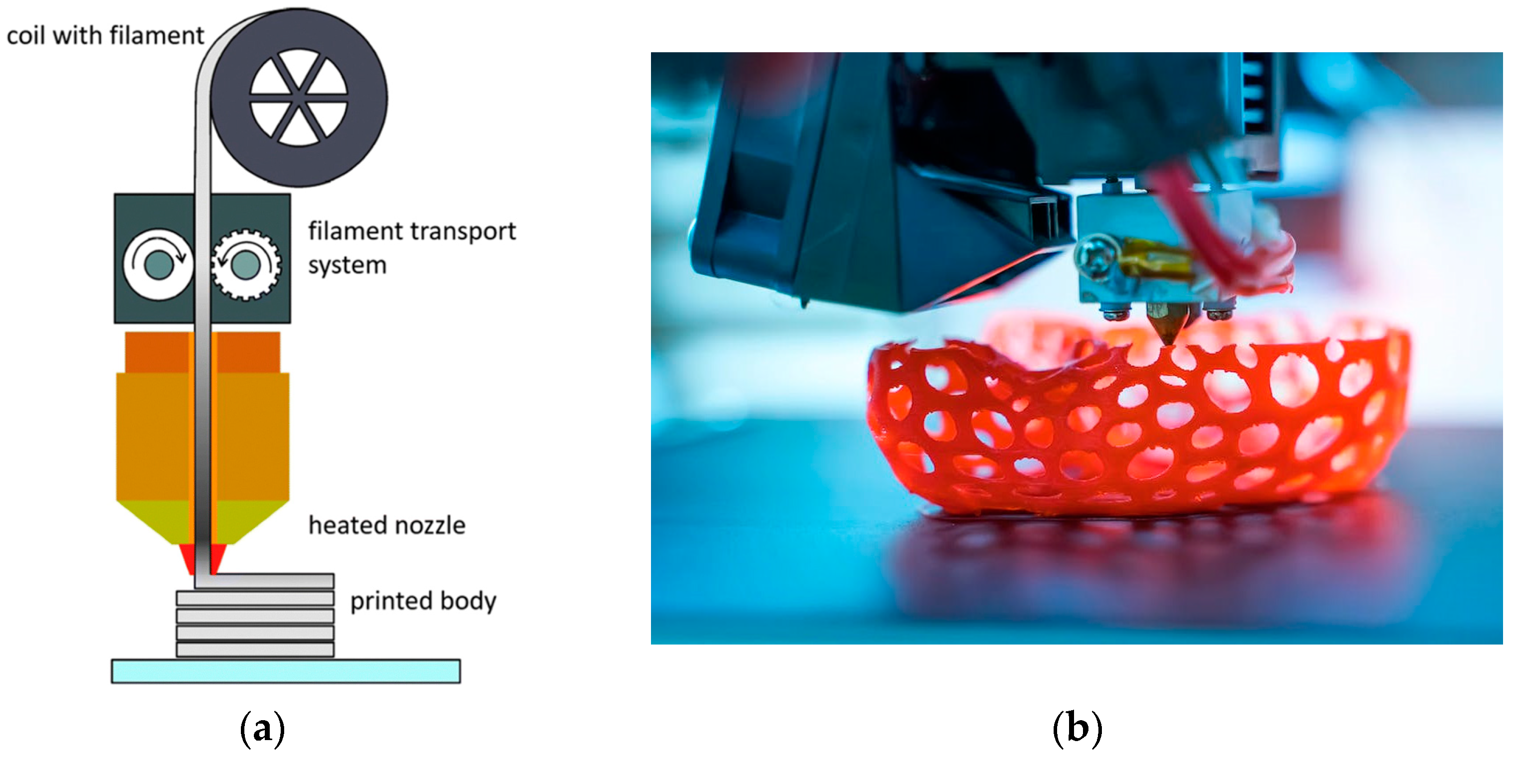
Figure 2.
Schematic representation of the DLP and SLA printing process.

Figure 3.
Example of metal 3D printing (a)—Example of dielectric SLS 3D printing (b).

Figure 4.
Example of metal MJ printing (a); Example of BJ printing (b). Arrows highlight moving axes.
Figure 4.
Example of metal MJ printing (a); Example of BJ printing (b). Arrows highlight moving axes.


Table 1.
Comparison of the FFF works examined.
| [#] | Description | Tech | Antenna Type | Frequency Band | Substrate | Conductive Material | Year |
|---|---|---|---|---|---|---|---|
| [11] | Compact 3-D-Printed Circularly Polarized Antenna for Handheld UHF RFID Readers | FFF | CP PIFA | 866 MHz | PLA | Copper tape | 2018 |
| [12] | 3-D-Printed Tunable Circularly Polarized Microstrip Patch Antenna | FFF | Patch antenna substrate | Variable depending on varactor diodes | ABS | Aluminum tape + silver epoxy for via holes | 2019 |
| [13] | Flexible and Stretchable Brush-Painted Wearable Antenna on a Three-Dimensional (3-D) Printed Substrate | FFF | Patch antenna substrate | 2.45 GHz | NinjaFlex | Silver conductive paste | 2017 |
| [14] | Wearable UHF RFID Sensor-Tag Based on Customized 3D-Printed Antenna Substrates | FFF | Enclosure for RFID sensor | 866 MHz | PLA | Copper tape | 2018 |
| [15] | Additively Manufactured Profiled Conical Horn Antenna With Dielectric Loading | FFF | Dielectric-loaded horn | 9–15 GHz | PLA | Copper electroplating | 2018 |
| [16] | Wideband Dual-Polarized 3D Printed Quad-Ridged Horn Antenna | FFF | Horn antennas | 4–13 GHz | PLA | Noise Hell SP-D-02 LACQUER™ | 2022 |
| [17] | Long-Slot Traveling-Wave Antenna Exhibiting Low Squint-Angle Variation over Frequency | FFF | Leaky-wave antenna | 31–35 GHz | PLA | Aluminum tape | 2022 |
| [18] | Antenna Gain Enhancement by Using Low-Infill 3D-Printed Dielectric Lens Antennas | FFF | Dielectric lens | 5G at 28 GHz | PLA | N/A | 2019 |
| [19] | 3-D-Printed Shaped and Material-Optimized Lenses for Next-Generation Spaceborne Wind Scatterometer Weather Radars | FFF | Dielectric lens | 13–25 GHz | PLA | / | 2022 |
| [20] | Novel Design Methodology for 3D-Printed Lenses for Travelling Wave Antennas | FFF | Dielectric lens | 26–29 GHz | PLA | / | 2022 |
| [21] | Dielectric Rod Antenna Array with Planar Folded Slot Antenna Excitation | FFF | Dielectric rod antenna array | 15 GHz | ABS | / | 2021 |
| [23] | Wideband Circularly Polarized 3-D Printed Dielectric Rod Antenna | FFF | Dielectric rod antenna array | 4–7.5 GHz | Preperm 10 | / | 2020 |
| [24] | Multibeam graded dielectric lens antenna from multimaterial 3-D printing | FFF | Dielectric lens | 5.8 GHz | Preperm + ABS | / | 2020 |
| [25] | 3D Printed OAM Reflectarray Using Half-Wavelength Rectangular Dielectric Element | FFF | Reflectarray | 28–32 GHz | Preperm 10 | Aluminum tape | 2020 |
| [26] | Dual Circularly Polarized 3-D Printed Broadband Dielectric Reflectarray With a Linearly Polarized Feed | FFF | Reflectarray | 26–40 GHz | Preperm 12 | / | 2022 |
| [27] | A 3D-Printed DRA Shared-Aperture Array for Low Cost Millimeter-Wave Applications | FFF | RDRA array | K/Ka Band | Preperm 12, 10 | / | 2022 |
| [28] | 3-D-Printed Wideband Multi-Ring Dielectric Resonator Antenna | FFF | Multiring DRA | 4.3–8.0 GHz | Preperm with various infill | / | 2019 |
| [29] | Dielectric Resonators Antennas Potential Unleashed by 3D Printing Technology: A Practical Application in the IoT Framework | FFF | LP DRA | 2.4–3.8 GHz | PLA+BaTiO3 | Copper tape | 2022 |
| [31] | Computational microwave imaging using 3D printed conductive polymer frequency-diverse metasurface antennas | FFF | Metasurface antenna for imaging system | 17.5–26.5 GHz | PLA | Electrifi | 2017 |
| [32] | Electromagnetic characterisation of conductive 3D-Printable filaments for designing fully 3D-Printed antennas | FFF | Various types of antennas and a T-resonator | 0.72–6 GHz | PLA | Electrifi | 2022 |
| [33] | Evaluating the Effectiveness of Planar and Waveguide 3D-Printed Antennas Manufactured Using Dielectric and Conductive Filaments | FFF | Circular waveguide wideband antennas | 3.2–4.2 GHz | PLA | Electrifi/Aluminum tape | 2023 |
Table 2.
Comparison of the SLA/DLP works examined.
| [#] | Description | Tech | Antenna Type | Frequency Band | Substrate | Conductive Material | Year |
|---|---|---|---|---|---|---|---|
| [34] | Direct 3-D printing of nonplanar linear-dipole-phased array antennas | SLA | Array of dipoles | 2.95 GHz | Resin | Copper electroplating | 2018 |
| [35] | 3-D Printed Horn Antennas and Components Performance for Space and Telecommunications | SLA | Tests on different antennas and waveguides | Resin | Copper electroplating | 2018 | |
| [36] | 3D Printed ‘Kirigami’-Inspired Deployable Bi-Focal Beam-Scanning Dielectric Reflectarray Antenna for mm-Wave Applications | SLA | Deployed reflectarray (kirigami inspired) | 26–34 GHz | Flexible Resin 80A | 2021 | |
| [37] | 3-D Printed Inhomogeneous Substrate and Superstrate for Application in Dual-Band and Dual-CP Stacked Patch Antenna | SLA | Substrate for a dual-band dual-CP patch antenna | 2.75; 3.25 GHz | Resin | 2018 | |
| [38] | Compact W-Band “Swan Neck” Turnstile Junction Orthomode Transducer Implemented by 3-D Printing | DLP | Turnstile waveguide junction | 75–110 GHz | Resin | Silver electroless plating | 2020 |
| [39] | A 3-D-Printed Wideband Circularly Polarized Parallel-Plate Luneburg Lens Antenna | SLA | GRIN Luneburg lens+horn antenna | 26.5–37 GHz | Resin | Copper foil | 2020 |
| [40] | A 3-D-Printed multibeam dual circularly polarized luneburg lens antenna based on quasi-icosahedron models for ka-band wireless applications | SLA | QICO Luneburg lens | Ka-band | Resin | 2020 | |
| [41] | Design and Manufacturing of Super-Shaped Dielectric Resonator Antennas for 5G Applications Using Stereolithography | SLA | Supershaped star DRA | 3.5 GHz | Resin | 2020 | |
| [43] | 3-D Printed Circularly Polarized Modified Fresnel Lens Operating at Terahertz Frequencies | SLA | Fresnel lens | 300 GHz | Resin | 2023 |
Table 3.
Comparison of the LPBF/DMLS/SLM/SLS works examined.
| [#] | Description | Tech | Antenna Type | Frequency Band | Substrate | Conductive Material | Year |
|---|---|---|---|---|---|---|---|
| [48] | Fabrication of a High-Efficiency Waveguide Antenna Array via Direct Metal Laser Sintering | DMLS | Waveguide antenna array | 2016 | |||
| [49] | 3-D Printed Metallic Dual-Polarized Vivaldi Arrays on Square and Triangular Lattices | DMLS | Ultrawide-band Vivaldi antenna array with SMPM connectors | 3–20 GHz | Titanium | 2020 | |
| [50] | A miniaturized three-dimensional log periodic Koch-dipole array antenna using T-shaped top loading | SLM | Log-periodic Koch dipole antenna array | 1–3.5 GHz | Alluminum alloy | 2021 | |
| [51] | Selective Laser Sintering Manufacturing as a Low Cost Alternative for Flat-Panel Antennas in Millimeter-Wave Bands | SLS | Waveguide antenna array | CNC compared with aluminum alloy | 2021 | ||
| [52] | 3-D-Printed Compact Wideband Magnetoelectric Dipoles With Circular Polarization | SLS | Folded magnetoelectric dipole | PC/ABS | Copper plated | 2018 | |
| [53] | 3-D Printed Monolithic GRIN Dielectric-Loaded Double-Ridged Horn Antennas | SLS | GRIN-loaded horn antenna | Nylon | Copper plated | 2020 |
Table 4.
Comparison of the BJ/Inkjet/MJ/miscellaneous works examined.
| [#] | Description | Tech | Antenna Type | Frequency Band | Substrate | Conductive Material | Year |
|---|---|---|---|---|---|---|---|
| [56] | Multilayer Inkjet Printing of Millimeter-Wave Proximity-Fed Patch Arrays on Flexible Substrates | Inkjet | Patch antenna and substrate | 2.45 GHz | Dielectric ink | Silver ink | 2013 |
| [57] | Inkjet Printing of Multilayer Millimeter-Wave Yagi-Uda Antennas on Flexible Substrates | Inkjet | Yagi-Uda | 25 GHz | Flexible substrate from Rogers | Silver ink | 2016 |
| [59] | 3-D Inkjet-Printed Helical Antenna with Integrated Lens | Inkjet Dielectric + Silver | Helical antenna integrated with a Fresnel lens | 8.8 GHz | 2017 | ||
| [60] | 3-D-Printed comb mushroom-like dielectric lens for stable gain enhancement of printed log-periodic dipole array | MJP | Mushrom lens antenna for log-periodic array | 14–20 GHz | Plastic powder | 2018 | |
| [61] | Mm-Wave Low-Cost 3D Printed MIMO Antennas with Beam Switching Capabilities for 5G Communication Systems | MJP | Mimo slot antenna array | Plastic powder | JetMetal technology for coating | 2020 | |
| [65] | Low-Loss 3-D Multilayer Transmission Lines and Interconnects Fabricated by Additive Manufacturing Technologies | AJP | Various microwave guide | up to 40 GHz | Dielectric ink | Silver ink | 2016 |
| [68] | 3D-Printed Low-Profile Single-Substrate Multi-Metal Layer Antennas and Array With Bandwidth Enhancement | Dragonfly | Patch antennas | Dielectric ink | Silver ink | 2020 | |
| [69] | Development of a Wideband and High-Efficiency Waveguide-Based Compact Antenna Radiator With Binder-Jetting Technique | BJ | Cavity antenna array | 13–16.5 GHz | Stainless steel | Sintering of the green made by BJ stainless steel | 2017 |
| [70] | Ka-Band Characterization of Binder Jetting for 3-D Printing of Metallic Rectangular Waveguide Circuits and Antennas | BJ | Different RF devices | Stainless steel | Sintering of the green made by BJ stainless steel | 2017 |
Table 5.
Advantages and disadvantages of different AM technologies.
| AM Technology | Advantages | Disadvantages |
|---|---|---|
| Fused Filament Fabrication (FFF) | Low cost, ease of use | Limited precision, rough surface finish, only thermoplastic polymers available |
| Vat-Polymerization (Stereolithography, Digital Light Processing) | High precision, good surface finish, low-to-medium initial costs | Limited material options |
| Selective Laser Sintering (SLS) | Wide range of materials, functional parts | High initial costs, rough surface finish |
| Selective Laser Melting (SLM)/Direct Metal Laser Printing (DMLP) | Direct metal production, critical applications | High initial costs, limited material options |
| Material Jetting | High precision, multiple material possibilities | High initial costs for equipment, variable cost for parts |
| Binder Jetting | Speed, multiple material possibilities | High initial costs for equipment, some post-processing required |
| Inkjet Printing | Precision, multiple material possibilities | High initial costs for equipment, limited material options, difficulty in handling high substrates |
| Aerosol Jet Printing | Fine electronics printing, versatility, five-axis printer | High initial costs for equipment, limited to small-scale production, variable cost |
Disclaimer/Publisher’s Note: The statements, opinions and data contained in all publications are solely those of the individual author(s) and contributor(s) and not of MDPI and/or the editor(s). MDPI and/or the editor(s) disclaim responsibility for any injury to people or property resulting from any ideas, methods, instructions or products referred to in the content. |
© 2024 by the author. Licensee MDPI, Basel, Switzerland. This article is an open access article distributed under the terms and conditions of the Creative Commons Attribution (CC BY) license (https://creativecommons.org/licenses/by/4.0/).
Share and Cite
MDPI and ACS Style
Chietera, F.P. Additively Manufactured Antennas and Electromagnetic Devices. Hardware 2024, 2, 85-105. https://doi.org/10.3390/hardware2020005
AMA Style
Chietera FP. Additively Manufactured Antennas and Electromagnetic Devices. Hardware. 2024; 2(2):85-105. https://doi.org/10.3390/hardware2020005
Chicago/Turabian StyleChietera, Francesco P. 2024. "Additively Manufactured Antennas and Electromagnetic Devices" Hardware 2, no. 2: 85-105. https://doi.org/10.3390/hardware2020005