Article

A Low-Power, Fast-Transient FVF-Based Output-Capacitorless LDO with Push–Pull Buffer and Adaptive Resistance Unit

1
Institute of Microelectronics of the Chinese Academy of Sciences, Beijing 100029, China
2
University of Chinese Academy of Sciences, Beijing 100049, China
*
Author to whom correspondence should be addressed.
Electronics 2023, 12(6), 1285; https://doi.org/10.3390/electronics12061285
Submission received: 13 February 2023 / Revised: 4 March 2023 / Accepted: 4 March 2023 / Published: 8 March 2023

Abstract

:
An output-capacitorless low-dropout regulator (LDO) with a push–pull buffer was presented in this paper. The proposed push–pull buffer was able to provide a large charge and discharge current to increase the slew rate at the gate of the power transistor effectively, thereby improving the transient response of this LDO. In addition, an adaptive resistance unit (ARU) was proposed to solve the right half-plane zero problem caused by Miller compensation to optimize the loop stability of the LDO. The proposed LDO was implemented in a 0.18-µm CMOS technology. Simulation results showed that the quiescent current of this LDO was only 16.1 µA. It regulated the output at 1.5 V from a 1.8 V supply, with a dropout voltage of 300 mV at the maximum output current of 50 mA. The maximum value of the voltage spike was 129 mV. Additionally, the recovery time of the LDO was 0.2 µs.

1. Introduction

Low-dropout (LDO) regulators are often used in power management mobile systems requiring small size and clean supply voltage. A traditional LDO always needs to connect a µF-level capacitor at its output pin to reduce output voltage spikes and ensure loop stability. However, with the miniaturization and portability of electronic equipment, the off-chip capacitance that occupies a large area is no longer allowed, so output capacitorless low-dropout regulator (OCL-LDO) recently became a new research direction [1,2,3,4,5,6,7,8,9].
There are many problems without the off-chip capacitor. The transient response problem is quite evident. When the load current suddenly decreases and the current supplied by the LDO does not have time to decrease accordingly, the excess current will charge the output voltage node, resulting in a rapid increase in the output voltage. This phenomenon is known as overshoot of the output voltage. Conversely, when the load current sharply increases, it will cause undershoot of the output voltage. Both overshoot and undershoot can cause instability in the LDO output voltage, which worsens the performance of the subsequent equipment; thus, suppressing voltage spikes caused by load changes has always been one of the main functions of the LDO [10,11,12,13,14,15,16]. Traditional LDOs tended to use large off-chip capacitors to suppress voltage spikes, while OCL-LDOs do not. In actuality, the transient response is dependent on a number of critical parameters such as the slew rate at the gate of the power transistor (SRG) and the loop bandwidth (BWL). The slew rate is a large-signal parameter related to the magnitude of the bias current, whereas the loop bandwidth involves small-signal parameters that significantly depend on the positions of the poles and the zeros in the feedback system.
Figure 1 shows one reported LDO structure used in [17,18,19,20,21,22] to enable OCL-LDO, the core for which was a flipped voltage follower (FVF). The advantages of FVF include low circuit complexity and short transient response loop in the case of small-signal response. However, if there is rapid and large change of load current (IO), the output-capacitorless LDO will experience a large-signal response. At this point, the slew rate of each node in the transient response loop, especially the node at the gate of the power transistor, becomes the main limitation of the transient response of the OCL-LDO, and the slew rate of most nodes is limited by its quiescent current. As shown in Figure 1, when the output voltage rises suddenly, Ibias1 charges the gate capacitance of the power transistor, so the maximum charging current is equal to the bias current Ibias1, and, conversely, when the output voltage drops, (Ibias2-Ibias1) is the maximum discharge current at the gate of power transistor. However, due to the large area of the power transistor, there is a large parasitic capacitance at its gate, and a small quiescent current is not enough to charge this capacitance rapidly. However, if the quiescent current is increased, it will lead to an increase in power dissipation. Therefore, a new structure is needed to solve this problem. Man et al. [20] reported using dynamic biasing to solve this problem. In [20], the output voltage (VOUT) was compared to the reference voltage (VREF) by a common-gate amplifier. Additionally, in order to inject and withdraw more current for charging and discharging during the transient instant, a push–pull circuit was used as the output stage of this amplifier. However, this structure was limited by the narrow common-mode input range and bandwidth of the common-gate amplifier. More power was required for common-gate amplifiers to detect fast voltage spikes to improve transient response significantly. Another researcher used the replica transistor of the power transistor to provide additional bias current when the load current increases [23,24], but there was a large bias current through the circuit when the output current was maximum, resulting in unnecessary power dissipation. Furthermore, Park et al. [2] reported an external transient enhancement circuit to provide a temporary bias current by capacitive coupling. It could be used not only for FVF-based LDOs, but also in a variety of LDO circuits. However, limited by the coupled capacitance and the matching resistor, this method often does not balance the speed and accuracy of charge and discharge. According to the brief review, it was evident that a structure is needed which can burst out large charging and discharging currents when the load current changes rapidly. Therefore, this work uses a push–pull buffer to meet the transient response requirements.
In addition, frequency compensation is another problem for OCL-LDO. Due to the large off-chip capacitance, traditional LDOs tend to set the dominate pole at the output voltage node, while OCL-LDO does not. So, a node is selected inside the OCL-LDO as the dominate pole. The gate of the power transistor is well suited as a node for setting the main pole due to its large parasitic capacitance. In addition, Miller compensation is used to further improve its stability. However, relying only on parasitic capacitance, the frequency of the dominate pole is not low enough to ensure loop stability; so, Miller compensation is used to further improve its stability. However, Miller compensation creates a right half-plane zero point, which threatens the stability of the system; so, it is necessary to select a suitable zeroing resistor. In this paper, an adaptive resistor unit (ARU) is proposed as the zeroing resistor for Miller compensation, which optimizes the loop stability in the load range.
In this paper, Section 2 introduces the structure and principle of the FVF-based push-pull buffer. Section 3 presents the frequency compensation in this work and introduces the adaptive resistor unit. The simulation results are presented in Section 4. Finally, the conclusion of this paper is given.

2. Optimization of Transient Response

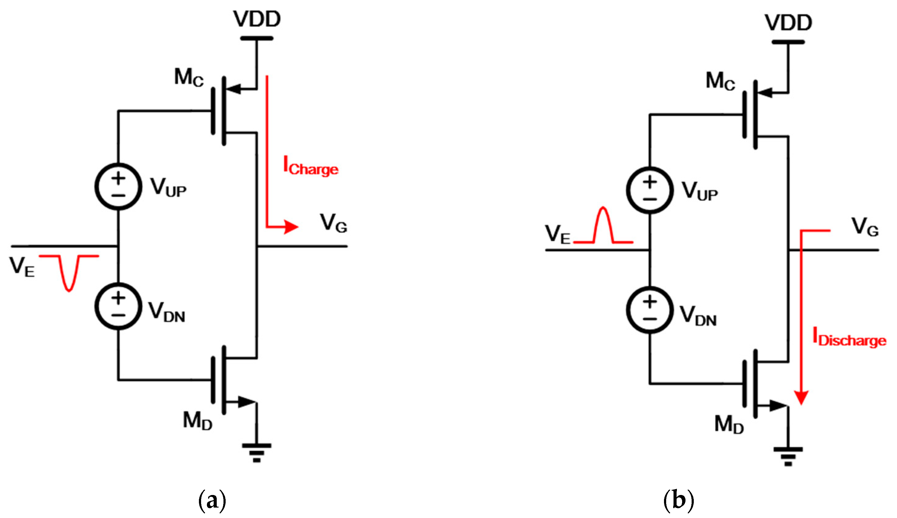
2.1. FVF-Based OCL-LDO

The LDO shown in Figure 1 was based on a flipped voltage follower (FVF) [25]. MP is the power transistor, while MC1 and MC2 form a folded error amplifier in the common-gate configuration [20]. VOUT, the output voltage, is controlled by a constant voltage source, VCTRL, when the bias current through MC1 is constant. VOUT is given by:
V OUT = V CTRL + V SG 1
where VSG1 is the source-to-gate voltage of MC1. Moreover, the voltage source is generated by the control-voltage generator circuit in Figure 2. An operational amplifier consists of a differential amplifier and a common-source amplifier, and then, it is connected to a unity-gain amplifier. In this way, the reference voltage, VREF, generated by the Bandgap circuit, is regenerated and has ability to drive the load consisting of MC3 and quiescent current source IDC. So, the control voltage, VCTRL, is given by:
V CTRL = V FB V SG 3 = V REF V SG 3
where VSG3 is the source-to-gate voltage of MC3. Since MC1 and MC3 are of the same size and of the same bias condition, the following relationship is achieved:
V OUT = V REF
when the output voltage changes, the source of MC1 senses change of the output voltage and eventually generates an error signal at the gate of the power transistor. The output impedance of the LDO is reduced drastically by the loop gain of the shunt feedback. Since there is no large output capacitor in an output-capacitorless LDO, the shunt feedback can push the pole created at the LDO output away from BWL. Therefore, the BWL of this LDO is wide and SRG is the dominate factor affecting the transient response of this LDO.

2.2. FVF-Based OCL-LDO

Figure 3 shows the structure of the push–pull buffer. VE is the error voltage signal generated by the comparison of output voltage and load voltage. VG is connected to the gate of the power transistor and two control signals, VGC and VGD, of the same phase are generated by two voltage sources, controlling the two output transistors MC and MD, respectively. In steady state (Vin remains stable), MC and MD pass only little quiescent current, which ensures a high efficiency of OCL-LDO at both light and heavy loads. As shown in Figure 3a, under large-signal responses, when VG rises rapidly, VGC and VGD affected by VG also rise rapidly, resulting in the MC transistor being off and MD receiving a large gate-to-source voltage. Therefore, a MD transistor can provide a large drain current to discharge the capacitance at the gate of the power transistor. Conversely, as shown in Figure 3b, when VG drops rapidly, MD will turn off and MC will turn on, and the parasitic capacitance at the gate of the power transistor can be quickly charged by Mc. The above discussion proves that the push–pull buffer has the ability to quickly charge and discharge capacitors; so, this work uses a push–pull buffer to increase the SRG.
Figure 4 shows the schematic of the push–pull buffer, with two source followers used to act as voltage sources in Figure 3. The source follower can provide a constant source-gate voltage VSG with a constant bias current. In addition, the source followers can reduce the equivalent impedance of the gate of MC and MD and push the poles generated at these two nodes, which is beneficial to the loop stability of this circuit.

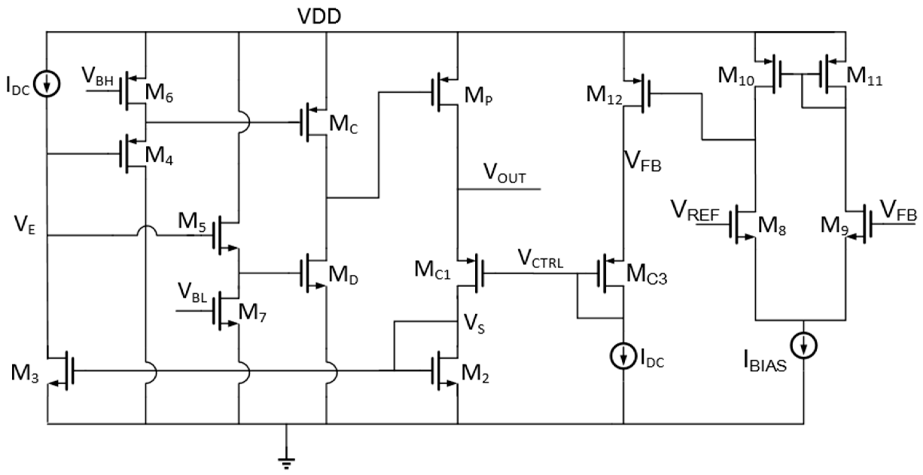
2.3. LDO with the Push–Pull Buffer

Figure 5 shows the overall structure of an FVF-based OCL-LDO with the push–pull buffer. The source of MC1 senses the drop (or increase) of VO and generates an error voltage signal at the drain of MC1. Since diode-connected transistors are used as the load, the swing range of vs. is similar to that of VOUT. The next stage uses a common-source amplifier loaded with a constant current source. The purpose of this stage is to first increase the DC gain of the negative feedback loop to compensate for the low DC gain of the FVF topology. Secondly, regarding the large-signal response, this structure enables VE to have a larger voltage swing range and increase the charge and discharge current of the push–pull buffer. Moreover, the current source IDC which supplies quiescent current to MC3 should match the one that provides quiescent current to M3 as much as possible to ensure that the output voltage VOUT is equal to the reference voltage VREF.

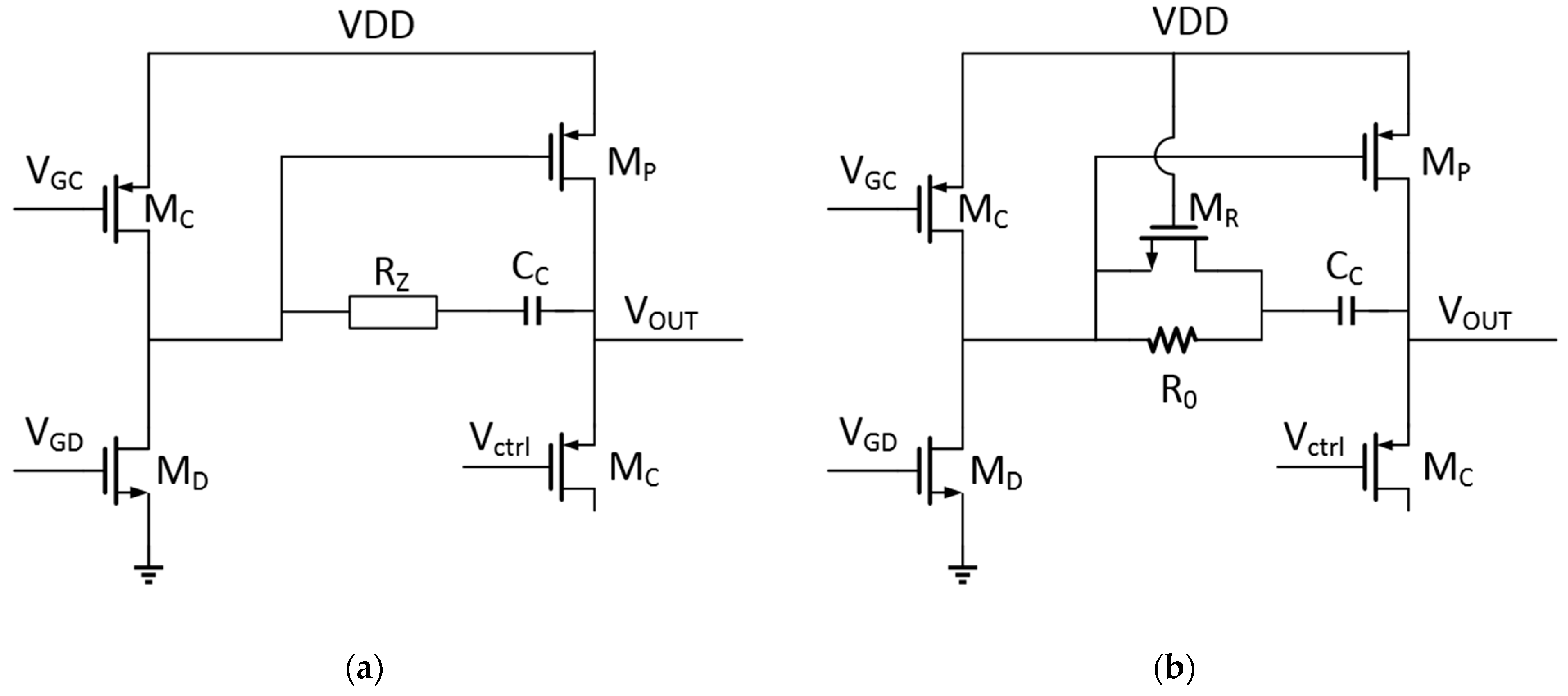
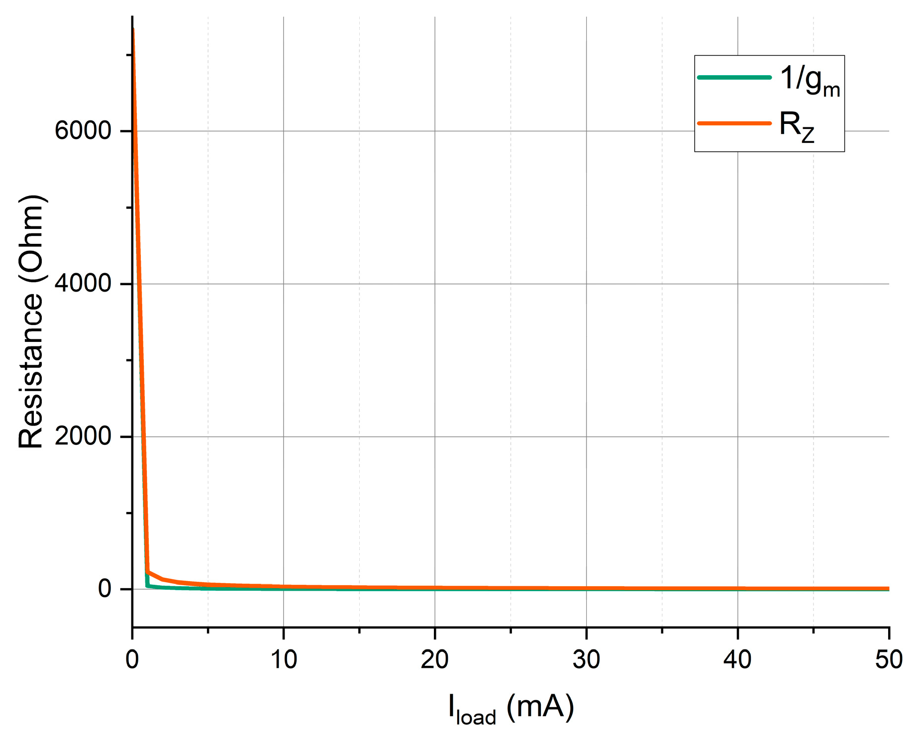
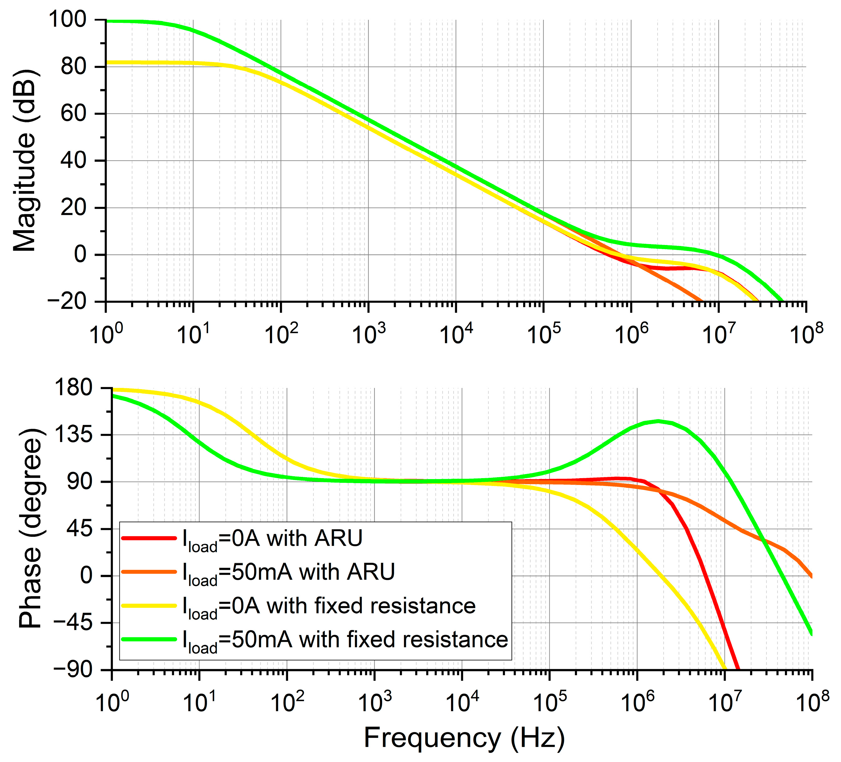
3. Optimization of Loop Stability

A large off-chip capacitor (often in the µF level) is always connected to the pin of VOUT in traditional LDOs, which creates a low-frequency pole at the output voltage node as the dominate pole. However, OCL-LDO has no off-chip capacitance, the pole created by the output voltage node is often the non-dominate pole. Furthermore, for FVF-based LDOs, the output impedance of the LDO is reduced by the loop gain of the shunt feedback, and the output poles are pushed further away. Thus, a low-frequency pole must be created as the dominate pole. The gate of the power transistor is an excellent node as the dominate pole position, because the area of the power transistor is quite large, resulting in a large parasitic capacitance. It allows the capacitance used for compensation to be reduced. Additionally, the push–pull buffer makes the impedance at the gate of power transistor large, and so, it is an excellent dominate pole position. If other nodes are selected as the dominate pole, it will come with the following risks. Firstly, the pole created by the gate of power transistor will threaten the loop stability as the non-dominate pole. Additionally, then, the compensation capacitor connected to the dominate pole will cause new slew rate problems in the case of large-signals response. Therefore, the gate of power transistor was selected as the dominate pole for this work. Miller capacitors are still needed to improve loop stability. As shown in Figure 6a, CC is the Miller capacitor. In addition, when VOUT overshoot or undershoot, CC can act as a coupling capacitor to regulate the gate voltage of power transistor. However, the Miller capacitor creates a right half-plane zero Z0, where Z0 is given by:
Z 0 = g mP / C C
where gmP is the equivalent transconductance of the power transistor. The right half-plane zero greatly affects the loop stability of this circuit, so a zeroing resistance RZ is always connected in series with the Miller capacitor. The position of Z0 becomes:
Z 0 = 1 ( 1 / g mP R Z ) C C
It can be observed from the above equation that the closer RZ and gmP are, the better the zeroing effect will be. However, gmP is a parameter related to the output current IO, which changes with the load, and the transconductance of the transistor operating in the saturation region is given by:
g m = μ C ox W L ( V GS V TH ) = 2 μ C OX W L I D
where µ is the carrier mobility, COX is gate oxide capacitance per unit area, VTH is the threshold voltage of the transistor and ID is the drain current. Transistors operating in the linear region can be used as resistors, and its resistance value is inversely proportional to the overdrive voltage. For example, in [26], a way of frequency compensation named pole-zero tracking was proposed, which used a transistor operating in the linear region as a variable resistor. So, in this work, a transistor MR operating in the linear region was used as the resistance, as shown in Figure 6b. The resistance of the transistor operating in the linear region RM was:
R M = 1 μ C OX W L ( V GS V TH )
From the above two formulas, it is evident that RM and 1/gm have the same trend with IO. Therefore, transistors operating in the linear region can be used as zeroing resistors.
However, when the output current is little, there is huge difference between the reciprocal of the actual transconductance of the power transistor and the actual equivalent resistance of MR. The reason for this is that the above equation is accurate only when the power transistor MP is operating in the saturation region and transistor MR is operating in the linear region. In most cases, the above two assumptions are true, except when the output current is very small. At light loads, the power transistor MP is in the subthreshold region and MR turns off. Therefore, both the transconductance of MP and the equivalent resistance of MR deviate from the calculated value, especially the latter. The equivalent resistance of MR in the cut-off region is much larger than that in the linear region. Consequently, a resistor R0 is paralleled across the MR. This structure is named adaptive resistance unit (ARU). When IO is small, the resistance of ARU, RZ is approximately equal to R0, and conversely, when IO is large, RZ is approximately equal to RM. R0 can effectively solve the problem of mismatch between the zeroing resistor and the transconductance of the power transistor at light loads. The comparison of 1/gm and RZ over the entire load current range is shown in Figure 7, and it was clear that their values were close in the whole load range. Additionally, the amplitude-frequency curve and phase-frequency curve using ARU and the fixed resistor are shown in Figure 8, it can be observed that when the fixed resistance was used as zeroing resistance, there was a right half-plane zero point located in the low frequency region at light loads, and there was a left half-plane zero point within the bandwidth at heavy loads. However, when ARU was used as the zeroing resistor, there were no zeros or poles except the main pole located within the bandwidth. So, it was proved that ARU had a significant improvement in loop stability.

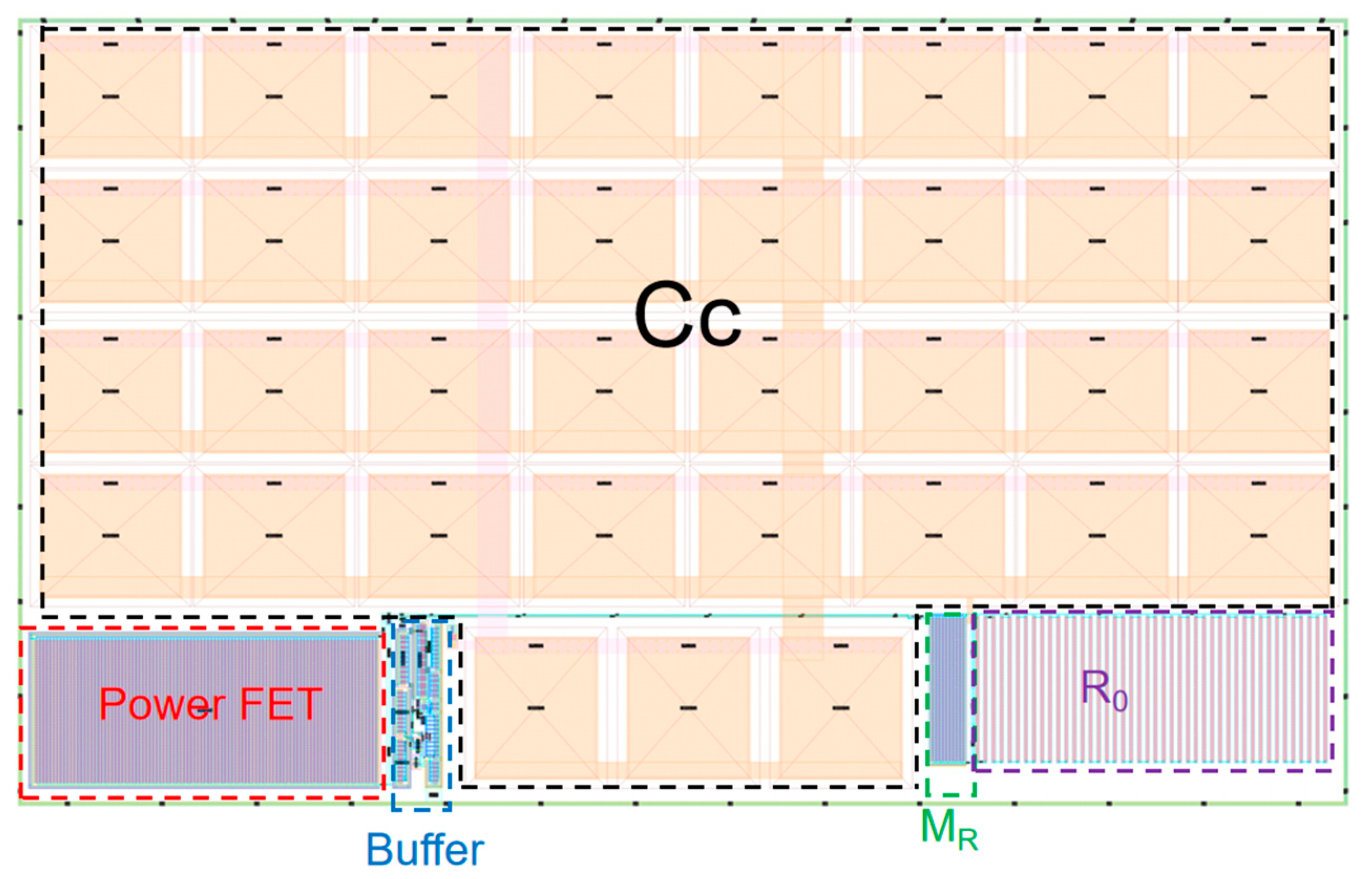
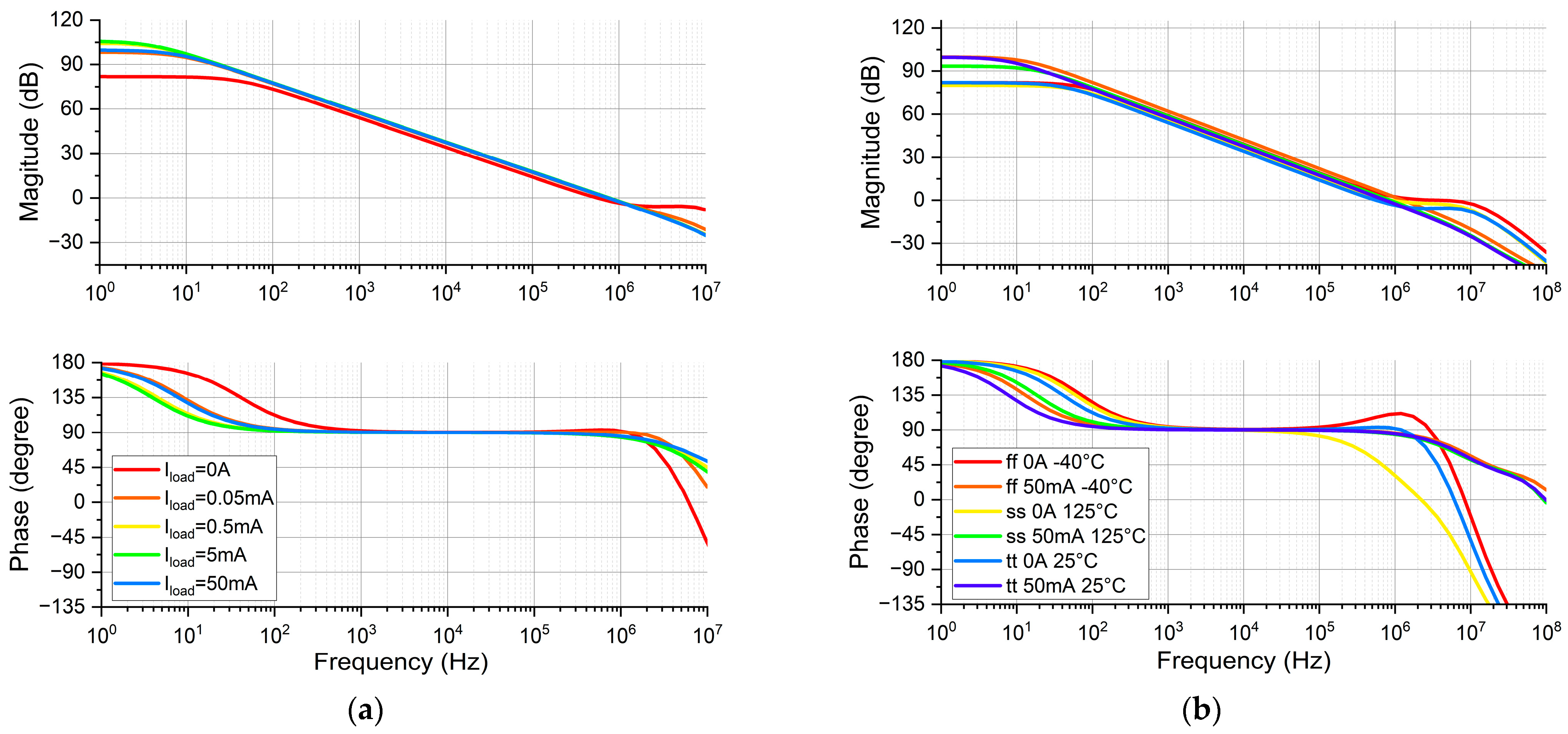
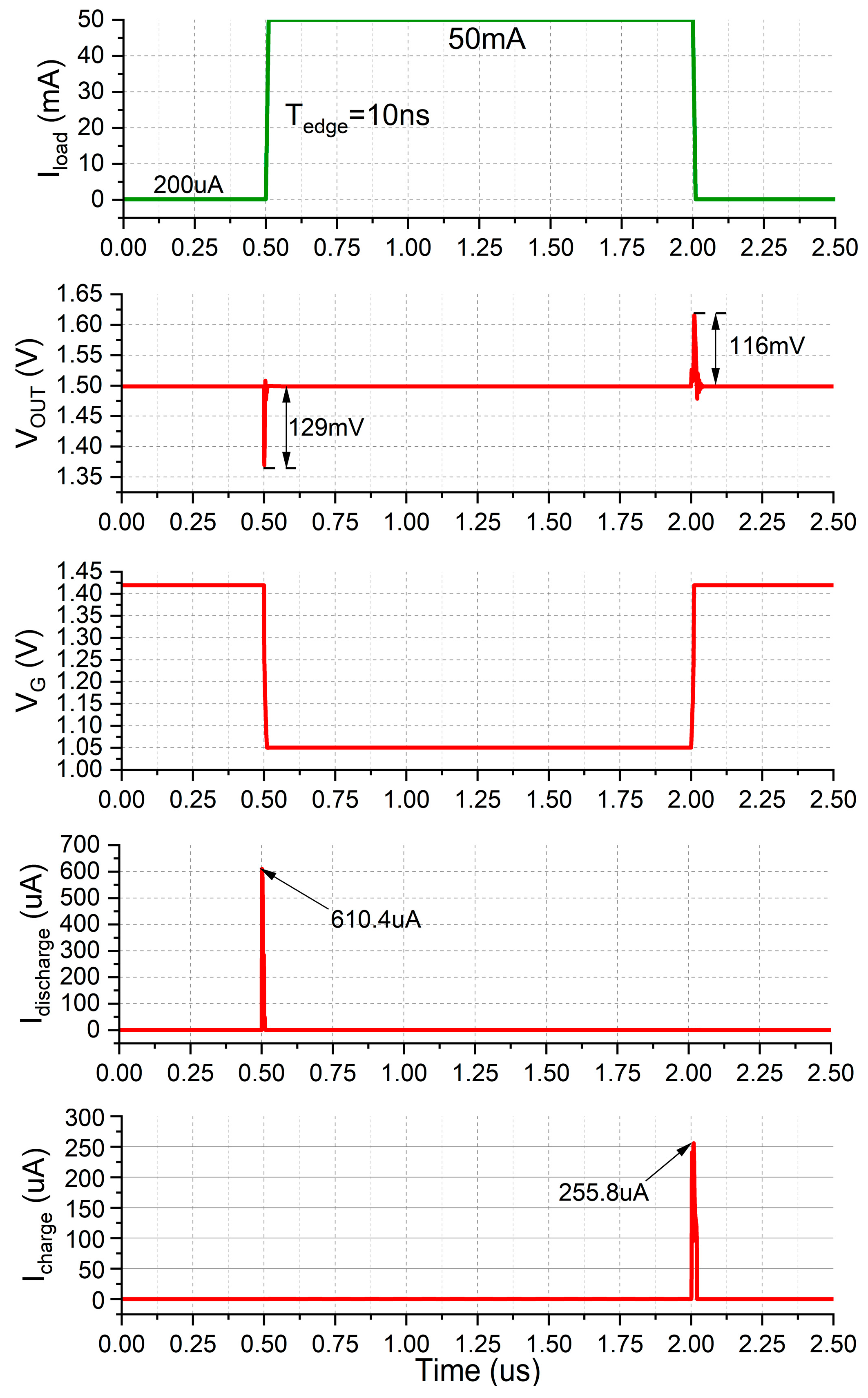
4. Simulation Result and Discussion

The OCL-LDO in this paper was created and simulated in a CMOS process. The layout is shown in Figure 9, and the whole layout had a total area of around 279.16 µm × 165.16 µm. The Miller capacitor CC which is within the black dashed frame was about 50 pF, so it cost a lot of area. CC only spanned the output stage composed of the power transistor, so a large Miller capacitor was required to maintain loop stability. In particular, the control voltage generator circuit and standard current source IDC are not shown in Figure 9. Due to matching considerations, they were placed with the Bandgap circuit of the power management system. This power management system included this OCL-LDO, matching Bandgap circuit, the current source circuit and another auxiliary circuit. MC3, which was matched with MC1, was placed in the buffer area in this figure. The post-simulation results are exhibited as follows:
The LDO had a dropout voltage of 0.3 V and could provide 50 mA of load current. Additionally, when output capacitor value ranged from 0 to 1 nF, the loop of LDO was stable. The OCL-LDO also used a negligible 16.1 µA of quiescent current when the load current reached 50 mA; at this point, its current efficiency was 99.97%. The current efficiency η is a common measure of LDO efficiency and its formula is:
η = I OUT I OUT + I Q
where IOUT is the output current and IQ is the quiescent current of the OCL-LDO. In addition, with a 50 pF output capacitor, the load regulation was simulated for VIN = 1.8 V and VOUT = 1.5 V, and this result is shown in Figure 10a, and the load regulation was 1.45 mV/A.
By incorporating a sinusoidal signal into a DC input voltage of 1.8 V and monitoring the result, the power supply rejection (PSR) can be simulated. Additionally, the PSR of the OCL-LDO with 50 pF output capacitor under various load currents is depicted in Figure 10b, where VIN = 1.8 V. The PSR in the low frequency region was approximately 51 dB.
The phase margin is an important parameter to measure the stability of the LDO loop, which can be seen from the amplitude-frequency curve and phase-frequency curve. Amplitude-frequency and phase-frequency curves under different load current are shown in Figure 11a, when CL = 50 pF. As can be seen from Figure 11a, the bandwidth was approximately 500 kHz and there were no zeros or poles except the main pole located within the bandwidth. Thus, the phase margin was nearly 90 degrees. It was indicated that the circuit was stable over the entire load current range. Figure 11b shows the amplitude-frequency and phase-frequency curves under different load current, temperature, and process corner. The worst combination of process corner, output current, and temperature was 0 A and 125° and the minimum value of the phase margin was 38 degrees. This proved the feasibility of the proposed OCL-LDO.
The load transient response was simulated when the output of the OCL-LDO was connected to a 50 pF capacitor. Additionally, the range of load current was from 200 µA to 50 mA, with the rise/fall time of 10 ns. At VOUT = 1.5 V, as shown in Figure 12, the maximum output voltage overshoot and undershoot were both less than 130 mV. The fluctuations in output voltage were roughly ±8.5%. Based on the high slew rate push–pull buffer, it was possible to produce the little overshoot or undershoot under large load-step. Additionally, then, as can be seen in Figure 12, the push–pull buffer can provide a 255 µA charge current and 610 µA discharge current in large-signal response. With large temporary charge and discharge currents, the gate of the power transistor can be quickly raised and lowered to control the output current of the OCL-LDO. As shown in Figure 12, the voltage at the gate of the power transistor VG varied with load from 1.05 V to 1.4 V. Moreover, the maximum value of recovery time was about 200 ns. Additionally, the LDO was able to accomplish the well-behaved settling characteristic due to the high phase margin over the entire load range.
As shown in Table 1, the proposed OCL-LDO showed improved performance when compared to several previously reported OCL-LDOs. The parameter known as the figure of merit, or FOM [10], which was used to measure transient response, is provided by:
FOM = T R I Q I LOAD _ MAX
where IQ is the quiescent current and ILOAD_MAX is the maximum output current. The response time, TR, is given by:
T R = C OUT Δ V OUT I LOAD _ MAX
where COUT is the equivalent resistance of the output node and ΔVOUT is maximum output spike voltage. It can be seen from Table 1 that the proposed LDO achieved a fast transient response and a low quiescent current.

5. Conclusions

This paper proposed a new structure of output-capacitorless LDO with low quiescent current and fast transient response. The flipped voltage follower topology was used to extend its bandwidth, and reduce the complexity of the LDO for fast response to load current transients. A push–pull buffer was implemented to increase the temporary charging and discharging currents at the gate of the power transistor in large signal transient response, ensuring the high slew rate at the gate of power transistor. In addition, an adaptable resistance unit was employed to solve the right half plane zero point problem caused by Miller compensation, which improved the loop stability over the entire load variation range. The LDO loop was stable over a load capacitance range of 0–1 nF. The simulation results showed that the maximum overshoot and undershoot voltage of the LDO was still less than 130 mV when the load current quickly changed from 200 μA to 50 mA within 10 ns, and Vout = 1.5 V. In addition, its quiescent current was only 16.1 μA. Low power and fast transient response made this output capacitorless LDO highly favorable for supply regulation of digital circuitry in small, portable devices.

Author Contributions

Conceptualization, Y.L. and L.W.; methodology, Y.L. and L.W.; software, Y.W. and S.W.; validation, Y.W. and S.W.; formal analysis, Y.L. and Y.W.; investigation, Y.L. and Y.W.; resources, S.W., M.C. and M.G.; data curation, Y.L., S.W., M.C. and M.G.; writing—original draft, Y.L.; writing—review & editing, Y.L.; visualization, M.C. and M.G.; supervision, L.W.; project administration, L.W.; funding acquisition, L.W. All authors have read and agreed to the published version of the manuscript.

Funding

This research received no external funding.

Data Availability Statement

The data used in this article is privacy.

Conflicts of Interest

The authors declare no conflict of interest.

References

  1. Zhao, J.; Gao, Y.; Zhang, T.T.; Son, H.; Heng, C.H. A 310-nA Quiescent Current 3-fs-FoM Fully Integrated Capacitorless Time-Domain LDO with Event-Driven Charge Pump and Feedforward Transient Enhancement. IEEE J. Solid State Circuits 2021, 56, 2924–2933. [Google Scholar] [CrossRef]
  2. Park, C.J.; Onabajo, M.; Silva-Martinez, J. External Capacitor-Less Low Drop-Out Regulator With 25 dB Superior Power Supply Rejection in the 0.4–4 MHz Range. IEEE J. Solid State Circuits 2014, 49, 486–501. [Google Scholar] [CrossRef]
  3. Lu, Y.; Wang, Y.; Pan, Q.; Ki, W.H.; Yue, C.P. A Fully-Integrated Low-Dropout Regulator With Full-Spectrum Power Supply Rejection. IEEE Trans. Circuits Syst. I Regul. Pap. 2015, 62, 707–716. [Google Scholar] [CrossRef]
  4. Chong, S.; Chan, P.K. A 0.9-/spl mu/A Quiescent Current Output-Capacitorless LDO Regulator with Adaptive Power Transistors in 65-nm CMOS. IEEE Trans. Circuits Syst. I Regul. Pap. 2013, 60, 1072–1081. [Google Scholar] [CrossRef]
  5. Torres, J.; El-Nozahi, M.; Amer, A.; Gopalraju, S.; Abdullah, R.; Entesari, K.; Sanchez-Sinencio, E. Low Drop-Out Voltage Regulators: Capacitor-less Architecture Comparison. IEEE Circuits Syst. Mag. 2014, 14, 6–26. [Google Scholar] [CrossRef]
  6. Sularea, I.; Răducan, C.; Neag, M. A Capacitor-Less LDO with High PSR over a Wide Frequency Range. In Proceedings of the 2021 International Semiconductor Conference (CAS), Sinaia, Romania, 6–8 October 2021; pp. 213–216. [Google Scholar]
  7. Li, R.; Zhang, X.; Zeng, Y.; Lin, Y.; Yang, J.; Tan, H.Z. High PSR Output-Capacitor-Less LDO with Double Buffers Technique. In Proceedings of the 2020 27th IEEE International Conference on Electronics, Glasgow, UK, 23–25 November; Circuits and Systems (ICECS): Glasgow, UK, 2020; pp. 1–4. [Google Scholar]
  8. Leo, C.J.; Raja, M.K.; Minkyu, J. An ultra low-power capacitor-less LDO with high PSR. In Proceedings of the 2013 IEEE MTT-S International Microwave Workshop Series on RF and Wireless Technologies for Biomedical and Healthcare Applications (IMWS-BIO), Singapore, 9–11 December 2013; pp. 1–3. [Google Scholar]
  9. Lim, Y.; Lee, J.; Lee, Y.; Song, S.-S.; Kim, H.-T.; Lee, O.; Choi, J. An External Capacitor-Less Ultralow-Dropout Regulator Using a Loop-Gain Stabilizing Technique for High Power-Supply Rejection Over a Wide Range of Load Current. IEEE Trans. Very Large Scale Integr. VLSI Syst. 2017, 25, 3006–3018. [Google Scholar] [CrossRef]
  10. Hazucha, P.; Karnik, T.; Bloechel, B.A.; Parsons, C.; Finan, D.; Borkar, S. Area-efficient linear regulator with ultra-fast load regulation. IEEE J. Solid State Circuits 2005, 40, 933–940. [Google Scholar] [CrossRef]
  11. Liu, X.; Krishnamurthy, H.K.; Na, T.; Weng, S.; Ahmed, K.Z.; Schaef, C.; Ravichandran, K.; Tschanz, J.W.; De, V. A Universal Modular Hybrid LDO With Fast Load Transient Response and Programmable PSRR in 14-nm CMOS Featuring Dynamic Clamp Strength Tuning. IEEE J. Solid State Circuits 2021, 56, 2402–2415. [Google Scholar] [CrossRef]
  12. Lu, Y.; Ki, W.H.; Yue, C.P. A 0.65ns-response-time 3.01ps FOM fully-integrated low-dropout regulator with full-spectrum power-supply-rejection for wideband communication systems. In Proceedings of the 2014 IEEE International Solid-State Circuits Conference Digest of Technical Papers (ISSCC), San Francisco, CA, USA, 9–13 February 2014; pp. 306–307. [Google Scholar]
  13. Duong, Q.H.; Kong, J.-W.; Shin, H.-S.; Nguyen, H.-H.; Kim, P.-J.; Ko, Y.-S.; Yu, H.-Y.; Park, H.-J. Multiple-Loop Design Technique for High-Performance Low-Dropout Regulator. IEEE J. Solid State Circuits 2017, 52, 2533–2549. [Google Scholar] [CrossRef]
  14. Magod, R.; Bakkaloglu, B.; Manandhar, S. A 1.24 uA Quiescent Current NMOS Low Dropout Regulator with Integrated Low-Power Oscillator-Driven Charge-Pump and Switched-Capacitor Pole Tracking Compensation. IEEE J. Solid State Circuits 2018, 53, 2356–2367. [Google Scholar] [CrossRef]
  15. Al-Shyoukh, M.; Lee, H.; Perez, R. A Transient-Enhanced Low-Quiescent Current Low-Dropout Regulator with Buffer Impedance Attenuation. IEEE J. Solid State Circuits 2007, 42, 1732–1742. [Google Scholar] [CrossRef] [Green Version]
  16. Ho, M.; Mak, K.L.; Leung, K.N. A Low-Power Fast-Transient 90-nm Low-Dropout Regulator with Multiple Small-Gain Stages. IEEE J. Solid State Circuits 2010, 45, 2466–2475. [Google Scholar]
  17. Li, R.; Zeng, Y.; Lin, Y.; Yang, J.; Tan, H.-z. High-PSR and fast-transient LDO regulator with nested adaptive FVF structure. In Proceedings of the 2020 IEEE International Conference on Integrated Circuits, Technologies and Applications (ICTA), Nanjing, China, 23–25 November 2020; pp. 51–52. [Google Scholar]
  18. Huang, M.; Feng, H.; Lu, Y. A Fully Integrated FVF-Based Low-Dropout Regulator with Wide Load Capacitance and Current Ranges. IEEE Trans. Power Electron. 2019, 34, 11880–11888. [Google Scholar] [CrossRef]
  19. Guo, J.; Leung, K.N. A 6µW Chip-Area-Efficient Output-Capacitorless LDO in 90-nm CMOS Technology. IEEE J. Solid State Circuits 2010, 45, 1896–1905. [Google Scholar] [CrossRef]
  20. Man, T.Y.; Leung, K.N.; Leung, C.Y.; Mok, P.K.T.; Chan, M. Development of Single-Transistor-Control LDO Based on Flipped Voltage Follower for SoC. IEEE Trans. Circuits Syst. I Regul. Pap. 2008, 55, 1392–1401. [Google Scholar] [CrossRef] [Green Version]
  21. Or, P.Y.; Leung, K.N. An Output-Capacitorless Low-Dropout Regulator with Direct Voltage-Spike Detection. IEEE J. Solid State Circuits 2010, 45, 458–466. [Google Scholar] [CrossRef]
  22. Cai, G.; Lu, Y.; Zhan, C.; Martins, R.P. A Fully Integrated FVF LDO With Enhanced Full-Spectrum Power Supply Rejection. IEEE Trans. Power Electron. 2021, 36, 4326–4337. [Google Scholar] [CrossRef]
  23. Lam, Y.H.; Ki, W.H. A 0.9V 0.35 µm Adaptively Biased CMOS LDO Regulator with Fast Transient Response. In Proceedings of the 2008 IEEE International Solid-State Circuits Conference—Digest of Technical Papers, San Francisco, CA, USA, 3–7 February 2008; pp. 442–626. [Google Scholar]
  24. Rincon-Mora, G.A.; Allen, P. A low-voltage, low quiescent current, low drop-out regulator. IEEE J. Solid State Circuits 1998, 33, 36–44. [Google Scholar] [CrossRef] [Green Version]
  25. Ramirez-Angulo, J.; Carvajal, R.G.; Torralba, A.; Galan, J.; Vega-Leal, A.P.; Tombs, J. The flipped voltage follower: A useful cell for low-voltage low-power circuit design. In Proceedings of the 2002 IEEE International Symposium on Circuits and Systems. Proceedings (Cat. No.02CH37353), Phoenix-Scottsdale, AZ, USA, 26–29 May 2002; p. III. [Google Scholar]
  26. Kwok, K.C.; Mok, P.K.T. Pole-zero tracking frequency compensation for low dropout regulator. In Proceedings of the 2002 IEEE International Symposium on Circuits and Systems (ISCAS), Phoenix-Scottsdale, AZ, USA, 26–29 May 2002; p. IV. [Google Scholar]
  27. Milliken, R.J.; Silva-Martinez, J.; Sanchez-Sinencio, E. Full On-Chip CMOS Low-Dropout Voltage Regulator. IEEE Trans. Circuits Syst. I Regul. Pap. 2007, 54, 1879–1890. [Google Scholar] [CrossRef]
  28. Ho, E.N.Y.; Mok, P.K.T. Wide-Loading-Range Fully Integrated LDR With a Power-Supply Ripple Injection Filter. IEEE Trans. Circuits Syst. II Express Briefs 2012, 59, 356–360. [Google Scholar] [CrossRef]
  29. Li, G.; Qian, H.; Guo, J.; Mo, B.; Lu, Y.; Chen, D. Dual Active-Feedback Frequency Compensation for Output-Capacitorless LDO with Transient and Stability Enhancement in 65-nm CMOS. IEEE Trans. Power Electron. 2020, 35, 415–429. [Google Scholar] [CrossRef]
  30. Yang, F.; Mok, P.K.T. A 65nm inverter-based low-dropout regulator with rail-to-rail regulation and over −20dB PSR at 0.2V lowest supply voltage. In Proceedings of the 2017 IEEE International Solid-State Circuits Conference (ISSCC), San Francisco, CA, USA, 5–9 February 2017; pp. 106–107. [Google Scholar]
Figure 1. Large-signal response of FVF-based LDO (a) charge (b) discharge.
Electronics 12 01285 g001
Figure 2. The schematic of control-voltage generator.
Electronics 12 01285 g002
Figure 3. Large-signal response of the push–pull buffer (a) charge (b) discharge.
Electronics 12 01285 g003
Figure 4. Circuit diagram of push–pull buffer.
Electronics 12 01285 g004
Figure 5. Full circuit diagram of the OCL-LDO with the proposed push–pull buffer.
Electronics 12 01285 g005
Figure 6. (a) The traditional Miller compensation. (b) Miller compensation with ARU.
Electronics 12 01285 g006
Figure 7. Comparison of RZ and 1/gm in the simulation.
Electronics 12 01285 g007
Figure 8. LDO loop gain and phase response with ARU and with fixed resistance.
Electronics 12 01285 g008
Figure 9. Layout of the proposed OCL-LDO.
Electronics 12 01285 g009
Figure 10. (a) Simulated load regulation. (b) Simulated PSR versus frequency under different load current (from 0 A to 50 mA).
Electronics 12 01285 g010
Figure 11. (a) Simulated amplitude-frequency and phase-frequency curves under different load current with CL = 50 pF. (b) Simulated amplitude-frequency and phase-frequency curves under different load current, temperature, and process corner with CL = 50 pF.
Electronics 12 01285 g011
Figure 12. Simulated load transient response of OCL-LDO and the charge/discharge current when VOUT is overshoot/undershoot and the voltage of the gate of power transistor VG.
Electronics 12 01285 g012
Table 1. Performance summary and comparison of OCL-LDO.
[27][28][2][4][29][30]This Work
Year2007201220142012202020172023
Technology (nm)350130180656565180
Chip Area (mm2)0.120.0180.140.0170.01050.0160.046
Input Voltage (V)31.21.81.20.95–1.20.61.8
Maximum Output Current (mA)5050501001005050
Quiescent Current (µA)6537.32550.9–82.4143216.1
Current Efficiency (%)99.8799.9399.8999.9999.9999.9499.97
On-chip Capacitor (pF)2321284.564050
Off-chip Capacitor (pF)100201000–100100400–1000
Settling Time (µs)150.4663.2N/A0.2
FOM (ps)0.2330.0170.2640.0560.03220.1370.0415
Disclaimer/Publisher’s Note: The statements, opinions and data contained in all publications are solely those of the individual author(s) and contributor(s) and not of MDPI and/or the editor(s). MDPI and/or the editor(s) disclaim responsibility for any injury to people or property resulting from any ideas, methods, instructions or products referred to in the content.

