


Quantum Nanomaterials for Advanced Nanoelectronics and Optoelectronics
A special issue of Nanomaterials (ISSN 2079-4991). This special issue belongs to the section "Nanoelectronics, Nanosensors and Devices".
Deadline for manuscript submissions: closed (31 December 2023) | Viewed by 951
Special Issue Editor

Interests: bosonics devices; nano-electronics; solid-state superfluid devices; optoelectronic 2D physics; RT quantum computing
Special Issue Information
Dear Colleagues,
We are happy to announce a special issue in the journal “Nanomaterials” entitled “Quantum nanomaterials for advanced nanoelectronics and optoelectronics”.
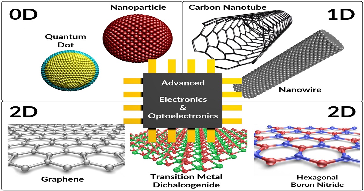
Tremendous research interest has been employed over the last few decades on quantum nanomaterials for the development of advanced nanoelectronics and optoelectronics applications. Low-dimensional quantum nanomaterials from zero-dimension (OD) to two-dimension (2D) exhibit extraordinary electronic, optical, excitonic, photonic, plasmonic, chemical, and thermal properties drastically different from the classical nature of three-dimensional (3D) materials. Exciting and novel quantum nanomaterial functionalities and new technology benchmarks are deemed necessary for advanced nanoelectronics and optoelectronics development in the future.
This special issue will focus on low-dimensional quantum materials such as (not limited to):
- 0D: Quantum dots, nanoparticles, 2D quantum dots, fullerenes, atomic clusters, etc;
- 1D: Carbon and non-carbon nanotubes, nanowires, nanoribbons, nanofibers, etc;
- 2D: vdWs materials (graphene, GO, hBN, TMDc, TMMs, BP, tellurene), oxide nanofilms, etc.
- Nanocomposites, inorganic-organic nanocomposite, nanoBio materials.
We invite original research articles/letters as well as review articles covering the current progress and future advances in the nanoelectronics and optoelectronics field including the following, but not limited to:
- Electronic properties and devices:
- Transistors, resistors, memory, magnetic, spintronic, sensor, diodes, piezoelectric, etc;
- Optoelectronic properties and devices:
- Phototransistors, photodetectors, LEDs, Solar cells, transparent conductors, etc;
- Optical properties include excitonic, plasmonic, photonic, spectroscopic, magneto-optic, etc;
- Magnetic, spintronic, and other novel physical properties.
A rapid publication (post-submission first decision in 12.7 days) and sincere attention to your manuscript will be provided. We look forward to receiving your exciting submissions.
Dr. Chandan Biswas
Guest Editor
Manuscript Submission Information
Manuscripts should be submitted online at www.mdpi.com by registering and logging in to this website. Once you are registered, click here to go to the submission form. Manuscripts can be submitted until the deadline. All submissions that pass pre-check are peer-reviewed. Accepted papers will be published continuously in the journal (as soon as accepted) and will be listed together on the special issue website. Research articles, review articles as well as short communications are invited. For planned papers, a title and short abstract (about 100 words) can be sent to the Editorial Office for announcement on this website.
Submitted manuscripts should not have been published previously, nor be under consideration for publication elsewhere (except conference proceedings papers). All manuscripts are thoroughly refereed through a single-blind peer-review process. A guide for authors and other relevant information for submission of manuscripts is available on the Instructions for Authors page. Nanomaterials is an international peer-reviewed open access semimonthly journal published by MDPI.
Please visit the Instructions for Authors page before submitting a manuscript. The Article Processing Charge (APC) for publication in this open access journal is 2900 CHF (Swiss Francs). Submitted papers should be well formatted and use good English. Authors may use MDPI's English editing service prior to publication or during author revisions.
Keywords
- quantum nanomaterials
- nanoelectronics
- optoelectronics
- graphene: graphite oxide
- transition-metal dichalcogenide
- hexagonal boron nitride
- quantum dots
- nanoparticles
- nanowires