Article

First Principles Study of the Photoelectric Properties of Alkaline Earth Metal (Be/Mg/Ca/Sr/Ba)-Doped Monolayers of MoS2

1
Xinjiang Laboratory of Phase Transitions and Microstructures in Condensed Matter Physics, College of Physical Science and Technology, Yili Normal University, Yining 835000, China
2
Physics and Electronic Engineering College, Kashi University, Kashi 844000, China
3
National Laboratory of Solid State Microstructures, School of Physics, Nanjing University, Nanjing 210093, China
*
Authors to whom correspondence should be addressed.
Molecules 2023, 28(16), 6122; https://doi.org/10.3390/molecules28166122
Submission received: 31 May 2023 / Revised: 30 July 2023 / Accepted: 9 August 2023 / Published: 18 August 2023
(This article belongs to the Special Issue Advanced Optical Materials for Photodetector and Energy Conversion)

Abstract

:
The energy band structure, density of states, and optical properties of monolayers of MoS2 doped with alkaline earth metals (Be/Mg/Ca/Sr/Ba) are systematically studied based on first principles. The results indicate that all the doped systems have a great potential to be formed and structurally stable. In comparison to monolayer MoS2, doping alkaline earth metals results in lattice distortions in the doped system. Therefore, the recombination of photogenerated hole–electron pairs is suppressed effectively. Simultaneously, the introduction of dopants reduces the band gap of the systems while creating impurity levels. Hence, the likelihood of electron transfer from the valence to the conduction band is enhanced, which means a reduction in the energy required for such a transfer. Moreover, doping monolayer MoS2 with alkaline earth metals increases the static dielectric constant and enhances its polarizability. Notably, the Sr–MoS2 system exhibits the highest value of static permittivity, demonstrating the strongest polarization capability. The doped systems exhibit a red-shifted absorption spectrum in the low-energy region. Consequently, the Be/Mg/Ca–MoS2 systems demonstrate superior visible absorption properties and a favorable band gap, indicating their potential as photo-catalysts for water splitting.

1. Introduction

Photocatalysts are frequently synthesized using materials with lower dimensions, such as graphene [1,2], hexagonal boron nitride [2], transition metal sulfides [3,4], and g-C3N4 [5], due to their high specific surface area, abundance of active catalytic sites, and high electron–hole separation rate [6,7]. Moreover, monolayer molybdenum disulfide (MoS2) is a widely researched excellent representative of two-dimensional (2D) materials with graphene-like structures. MoS2 is highly valued in the fields of photocatalysis, solar energy conversion, photovoltaics, and optoelectronics due to its optimal band gap, exceptional carrier mobility, and superior current-switching performance [8,9,10,11]. MoS2 is a layered material with an S–Mo–S sandwich structure, where a central layer of Mo atoms is flanked by two layers of S atoms above and below [12]. Monolayer MoS2 possesses a direct bandgap [13], enhancing its efficiency for water splitting. However, the efficient utilization of sunlight by 2D materials is limited by quantum size effects [14]. Substitution doping is an effective step to enhance the electronic properties of 2D materials’ device applications, similar to their use in conventional semiconductors [15,16,17,18,19]. Monolayer MoS2-doped Mn, Fe, Co, and Zn, for instance, as diluted magnetic semiconductors, could be applied in memory devices, store and read hard disks or MRAM [20,21]. P-type Au-doped MoS2 is applied in gas-sensing devices [22]. Re–MoS2, Mn–MoS2, Fe–MoS2 and Zn–MoS2 [16,23] have been used as n-type semiconductors, and Nb–MoS2 has been excellently applied in p-type semiconductors in optoelectronic devices, such as photodetectors and optical modulators, etc. The compounds mentioned in the above paragraph have all been synthesized experimentally. The experimental measurement analysis of the compounds has demonstrated that doping transition metal elements can induce a transformation from the intrinsic state to either n-type or p-type states in monolayer MoS2, which allows the noble compounds to be applied to different devices.
Moreover, the results of the first principles calculation and experimental test analyses of Co2+ (or Ni2+)-doped MoS2 all show that the introduction of Co2+ or Ni2+ results in the enhancement of monolayer MoS2 photocatalysis [24,25]. The prediction of the first principles computation of monolayer MoS2’s optical properties is consistent with experimental results. The conclusion indicates that doping impurities enhance monolayer MoS2 photocatalysis, and the first principles simulation method is a credible method.
The impurities mentioned in the above examples are transition metals. However, transition metal doping cannot reduce the bandgap to a lower width because of its local d orbital. The alkaline earth metals, including Be, Mg, Ca, Sr, Ba and others, constitute the second group of elements in the periodic table. In contrast to transition metal doping, alkaline earth metals do not involve localized d orbitals, so the doping of alkaline earth metals can effectively reduce the optical threshold energy of semiconductors [26]. The electronic structures of 2D materials with a graphene-like structure can be modified by the incorporation of alkaline earth metals. Studies conducted by Ullah [27] et al. and Tayyab M. [28] have demonstrated that doping graphene with Be and Mg can effectively modulate its band gap. Kumar G. M. [29] employed a hydrothermal method to synthesize Sn0.98Mg0.02S2 nanosheets and observed a red-shift in the absorption spectrum, indicating an enhanced absorption of visible light. Ani A. et al. [30] proposed that Ca-doped SnSe2 monolayers exhibit superior photocatalytic capacity. Doping graphene, or two-dimensional graphene-like materials, such as sulfur groups, with alkaline earth metals, has been demonstrated to induce minor defects that impact the electronic structure. This ultimately leads to an increase in carrier mobility and the improvement of absorption in visible light. It is postulated that the incorporation of alkaline earth metals can effectively modulate the photoelectric properties of monolayer MoS2. However, a systematic investigation into the impact of alkaline earth metals on the optoelectronic properties of monolayer MoS2 has yet to be conducted. Therefore, it is worthwhile to delve deeply into the mechanisms and regulatory laws governing its stable existence.
To sum up, monolayer MoS2, a semiconductor material, has been widely studied and applied, but the effective utilization of sunlight is limited by its electronic mobility, which is restricted to the finite sizes of the synthesized monolayer MoS2. It is found that the doping of alkaline earth metals (Be/Mg/Ca/Sr/Ba) can change the electronic band structure of the pristine materials and affect the transport of electrons. However, the effect of the alkaline earth metal doping of MoS2 on the photoelectric performance of the system has not been systematically theoretically studied. In our work, the energy band structure, density of states, and optical properties of monolayer MoS2 doped with alkaline earth metals were systematically studied based on first principles. The results show that the Be/Mg/Ca-MoS2 systems had superior visible absorption performance and ideal band gaps, and the potential to be used as photocatalyst candidates for water splitting.

2. Results

2.1. Analysis of Lattice Constants and Bond Population

The GGA-PBE calculation method was used to optimize the systems’ geometry. The lattice constants optimized were a = b = 3.17 and c = 12.43; the errors relative to the experimental values [31] and those of Hu [32] et al. were within 1%, which indicates that the computational methods and parameters used in this paper are reliable. Table 1 summarizes the optimized crystal structures of monolayer MoS2 and X-MoS2 systems. The formation energy of the doped system is an indicator of the degree of formation difficulty. A lower formation energy implies that the doped system more easily forms. The formation energy is calculated as:
E f = E d o p e d E u n d o p e d + n μ M o n μ X
E d o p e d and E u n d o p e d are the total energy of doped and undoped MoS2, μ M o and μ X are the chemical potential of the Mo and X atoms, while n denotes the number of X atoms doped into the supercell [10]. As shown in Table 1, the formation energy of the doped systems decreased gradually with the decrease in the doped atoms’ radius (RBa > RSr > RCa > RMg), which suggest that the smaller the atomic radius of the doped system was, the more easily the system formed. In Table 1, the absolute value of the formation energy of all the doped systems is shown within a reasonable range. The compounds with an absolute value of formation energy in that range can be synthesized via experiments [33,34,35,36,37]. Therefore, it can be inferred that all the doped systems can be synthesized. The Mg–MoS2 system exhibited the lowest formation energy among the five, indicating its superior suitability to formation.
According to reference [38], the covalent properties of a chemical bond become stronger as the value of the bond population increases. The results presented in Table 1 demonstrate that the maximum population of Mo–S bonds in each doped system surpassed that of the monolayer MoS2 system, while the minimum Mo–S bonding population in all doping systems was lower than that of the intrinsic system. However, the maximum value varied much more than the minimum value, which demonstrates that the stability of the doped systems was not destroyed by the introduction of impurity atoms.
The higher the Δγ value, the more pronounced the distortion of the corresponding system becomes [39]. In the table, we can see that the Δγ values of all doped systems were greater than that of a pure one, which implies that all the systems were distorted, and this aligns with the conclusion that the band gaps of the doped monolayer MoS2 were reduced. Moreover, Ba–MoS2 had the greatest degree distortion, which corresponds to its having the smallest bap gap. The optimized Mo–S bond length of 2.41 coheres with the one Li et al. reported [40]. It was observed that the Δγ values of the doped systems, except Be–MoS2, increased as the radius of the dopant atom increased. It was suggested that the degree of lattice distortion also increased with the dopant atom’s radius. The lattice distortion caused a separation between the positive and negative charge centers within the defect, which resulted in the creation of an internal electric dipole moment and a local potential difference. The introduction of alkaline earth metal elements was found to increase the rate of separation of photogenerated electron–hole pairs and decrease the energy needed for electron leap, as reported in reference [41].
In order to further verify its thermal stability, the AIMD (Ab Initio Molecular Dynamics) [42] analysis of monolayer MoS2 molybdenum and X–MoS2 systems was performed, and the temperature was set to room temperature (300 K), as shown in Figure 1. It can be seen that after 8000 steps of AIMD, with a time step of 1 fs, the structures of the six systems remained stable—there was no bond breaking, and the energy fluctuation was very small. The results show that the monolayer MoS2 and X-MoS2 systems have high stability at room temperature (300 K) [43,44].

2.2. Band Structures

The band structures of the monolayer MoS2 and X–MoS2 systems are presented in Figure 2. The Fermi energy level was set at 0 eV, and the energy range of −3~3 eV was selected for comparative analysis. The band structure of the monolayer MoS2 system is illustrated in Figure 2a; the conduction band minimum (CBM) and valence band maximum (VBM) are both located at the high symmetry point K. The semiconductor exhibited a direct band gap of 1.75 eV. This value was only 0.57% off from the experimental value of 1.74 eV [45], and was similar to the calculated value of 1.78 eV found in the literature [46].
Figure 2b–f illustrates the band structure of MoS2 doped with alkaline earth metals in a clear and concise manner, providing valuable insights into its electronic properties. The CBM and VBM of the doped systems exhibited a downward shift in energy compared to those of the monolayer MoS2. The X–MoS2 systems had band gaps of 1.68, 1.73, 1.62, 1.48, and 1.25 eV, which were observed to be reduced as the atomic numbers of doped alkali earth metal elements increased, except for Be. The decrease in the band gap indicated an effective reduction in the energy required for electron transition, thereby enhancing electron mobility. The doped systems displayed a series of impurity energy levels that were relatively independent, acting as an intermediary for valence band electrons to transition into the conduction band and enhancing the probability of electron transition to the conduction band. The doped systems were found to possess an enhanced optical absorption capacity. Notably, Ba–MoS2 exhibited the smallest direct band gap, indicating a minimal energy requirement for electron transition in this system. Therefore, it can be inferred that Ba–MoS2 boasts superior optical absorption capabilities.
In the doped systems exposed to visible light, valence electrons were induced to transition between valence and impurity levels as well as conduction bands, leading to the generation of photonic electron–hole pairs. The relatively independent impurity levels effectively reduced the probability of the electron–hole pairs’ recombination, and enhanced optical absorption capacity.

2.3. Density of States

The density of state (DOS) plots for monolayer MoS2 and X–MoS2 systems are presented in Figure 3, encompassing energies ranging from −3 to 3 eV. In Figure 3a, the densities of states in a monolayer MoS2 are depicted, wherein the conduction band is dominated by Mo–4d, Mo–5s, and S–3p states, and the valence band is dominated by Mo–4d, S–3s, and S–3p states. Both the CBM and VBM were mainly determined by the Mo–4d and S–3p states, which is consistent with what has been found in the literature [10].
Figure 3b–f display the DOS plots of the MoS2 systems doped with Be, Mg, Ca, Sr, and Ba, respectively. As illustrated in Figure 3b–d, in the Be/Mg/Ca-doped systems, the valence bands were mainly composed of Mo–4d and S–3p. The CBM was primarily derived from Mo–4d and S–3p states, with minor contributions from Be–2s, Mg–2p, Mg–3s, and Ca–4s states. The Ca–4s state had almost no effect on the conduction band. The Be–2s, Mg–3s, and Ca–4s states led to impurity levels near and above the Fermi level. The band gaps of the materials were narrowed due to impurity doping, which is consistent with the result regarding band structure. The DOS values of the Sr/Ba-doped MoS2 systems reveal that the effects of Sr–3d and Ba–3d states on the conduction band were more significant. The introduction of impurities into the materials led to a reduction in the band gaps, which is consistent with the results obtained from band structure analysis. The valence bands of the Sr/Ba-doped MoS2 systems were determined by the Mo–4d, S–3p, and S–3s states, while the Ba–5p state manifested a weak peak in the lower valence band of the Ba–MoS2 system, similarly to the results of other doped systems. The band gap of the Ba-doped system is the smallest. In Section 2.1, we can see that the Δγ value of Ba–MoS2 was the smallest, which demonstrates that Ba–MoS2 manifested the greatest degree of lattice distortion. This is why Ba–MoS2 had the smallest bandgap [10].
The contributions of S or d-state electrons from doped elements near and above the Fermi level are particularly obvious; they determine the impurity level, which causes the conduction band minimum (CBM) and valence band maximum (VBM) in the doped systems to shift down significantly, reducing the band gap, and ultimately leading to a decrease in photon excitation energy and a red shift in the predicted absorption spectrum of the doped systems.
To investigate the microscopic changes in energy levels of each system, we created LUMO (Lowest Unoccupied Molecular Orbital) and HOMO (Highest Occupied Molecular Orbital) diagrams for the monolayer MoS2 and X–MoS2 systems. Figure 4 shows the LUMO and HOMO, represented by the red and green areas, respectively. The isosurface was set as 0.04 e/Å3. The larger the area, the greater its ability to gain (lose) electrons. The LUMO orbitals possessing lower energy levels were more conducive to the obtaining of electrons, whereas the HOMO orbitals with higher electron energies were more likely to show electron loss [47]. In Figure 4a, we can see that the LUMO and HOMO of the monolayer MoS2 were distributed symmetrically, indicating that the centers of the positive and negative charges were in the same position, and there was no internal electric field. According to Figure 4b–f, compared to the monolayer MoS2, the LUMO and HOMO maps of the doped systems were redistributed, mostly clustered around the Mo and S atoms near the dopant atoms. In Figure 4b, the area of the HOMO of Mo is greater than that of the LUMO of S atoms near the Be atom, indicating that Mo and S lost and gained electrons, respectively, and electrons were easily transferred from the Mo atom to the S atom. In Figure 4c, we can see that the Mo atoms of the Mg–MoS2 had the greatest ability to gain electrons, while in the Ca–MoS2 system, Mo and S showed almost equal electron gain and loss. The Mo atoms in the Sr–MoS2 and Ba–MoS2 systems showed the greatest electron loss. The observed charge transfer and asymmetric distribution are in agreement with the findings of the static dielectric constant below.

2.4. Work Functions

To investigate charge transfer in monolayer MoS2 before and after doping, the work functions of monolayer MoS2 and X–MoS2 systems were calculated. The work function, as illustrated in Formula (2), is defined as the minimum energy required for an electron to transition from the Fermi energy level to the vacuum layer [48].
Φ = E v a c E F
where Φ represents work function, E v a c is vacuum level, and E F denotes Fermi level. The work function of the monolayer MoS2 was 4.79 eV, as shown in Figure 5a, which is consistent with the value of 4.89 eV calculated by Wei [49]. The Be/Mg/Ca/Sr/Ba-doped systems had lower work functions than that of the monolayer MoS2 (4.42, 4.35, 4.65, 4.54, and 4.64 eV, respectively). It was shown that doping with alkaline earth metals effectively reduced the energy required for electrons to escape from the interior to the semiconductor surface. Hence, the doped systems exhibited a better capacity for electron transition.

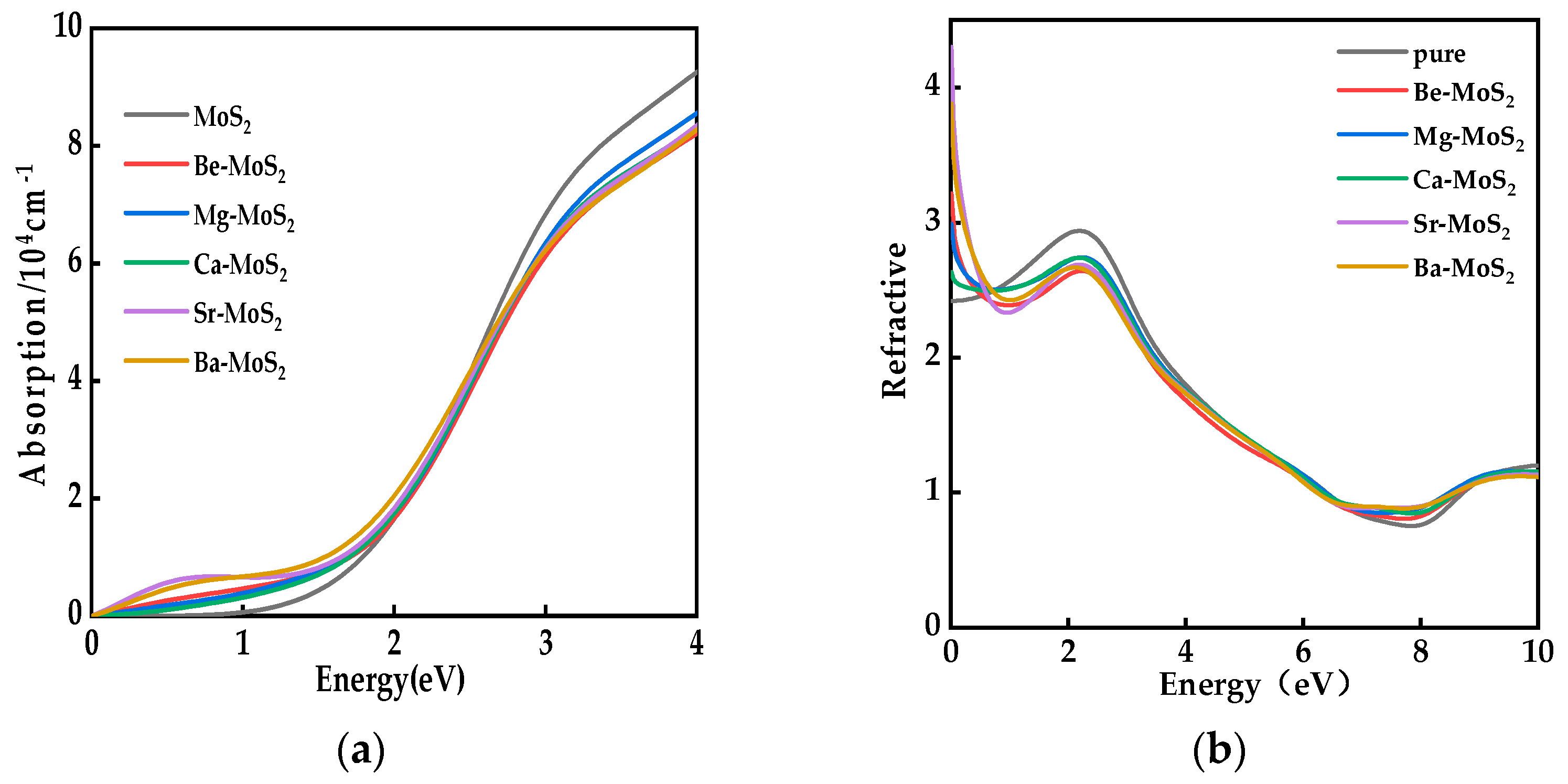
2.5. Optical Properties

Figure 6a shows the real part of the dielectric function (ε1) of monolayer MoS2 and X–MoS2 systems. The real part reflects the polarization strength of the semiconductor material in the presence of an external electric field with a change in incident photon energy. A higher value of ε1 indicates an enhancement in the capacity of the systems to bind charges, thereby increasing their polarizability [50]. When the incident photon energy was 0 eV, the systems exhibited a static dielectric constant (ε0). From Figure 6a, we can see that the ε0 values of the monolayer MoS2 and the doped systems were 5.88, 10.31, 8.89, 7.05, 18.20, and 14.94, respectively. In comparison to the monolayer MoS2, all the doped systems showed an increase in values of ε0, indicating an enhancement in the polarizability of the X–MoS2 systems. Therefore, in doped systems, the migration and separation rates of joint electron–hole pairs were accelerated, leading to an improvement in the optical performance of the system. The Sr–MoS2 system exhibited the highest values, indicating that it possessed the strongest polarization, excitation strength, and charge binding capability.
In Figure 6b, the imaginary parts of the dielectric function (ε2) of the monolayer MoS2 and doped systems are shown, varying with incident photon energy. The larger the values of ε2, the greater the probability of photon absorption, and the stronger the absorption energy of the materials. The value of ε2 is dependent on the number of electrons in the excited state, which increases the likelihood of the next transition occurring [50]. It can be observed that the ε2 of the monolayer MoS2 displayed a dielectric absorption peak at approximately 2.90 eV. This peak can be primarily attributed to the interband transition between the S–3p and Mo–4d states of electrons. The dielectric peaks of ε2 in the X–MoS2 systems were shifted towards the low-energy region compared to the monolayer MoS2. In the low-energy region, the intensity of the imaginary peak was significantly higher in the doped systems than in the intrinsic system. Because of a higher number of electrons present in the impurities formed by the doped system near the Fermi level, an enhancement in the light absorption of the doped systems in the low-energy region was observed. In the X–MoS2 systems, ε2 exhibited a significant response at a photon energy of 0 eV due to the partial occupation of energy levels of dopant atoms and the impurity energy levels straddling the Fermi energy levels. The presence of dopant elements facilitated electron transfer between multiple degenerate impurity levels, thereby enhancing the low-energy photon absorption of MoS2.
The absorption spectra and refractive indices of monolayer MoS2 and X–MoS2 systems are presented in Figure 7. As depicted in Figure 7a, in comparison to the monolayer MoS2, the doped systems displayed notable redshifts, and their light responses were extended to the low-energy region. Therefore, the doped systems showed a better light absorption capacity. The Sr–MoS2 and Ba–MoS2 systems displayed the same absorption peaks in the low-energy region (0–1.6 eV), demonstrating the two systems had strong capacity to use visible light.
Based on the refractive index curves depicted in Figure 7b, it can be inferred that the static refractive index of the monolayer MoS2 was 2.452 when the photon incident energy was 0 eV. This value is consistent with the theoretical value of 2.475 [51]. After doping, the static refractive index values of the X–MoS2 systems were all greater than that of the pure system. However, with the increase in incidence photon energy, the refractive indices of all systems tended to overlap and approach unity, which indicates that the monolayer MoS2 remained transparent both before and after doping.

2.6. Band Alignment

To understand the effects of alkaline earth metal doping on the photocatalytic capacity of the monolayer MoS2, the band alignments of both the monolayer MoS2 and X–MoS2 systems were calculated, and are illustrated in Figure 8. We used the concept of semiconductor electronegativity [52] to determine the redox and oxidation potentials for each water system. The position of the band edge was calculated using the Milligan electronegativity equation, which is illustrated in [53,54,55].
E V B M = χ E e l e c + 0.5 E g
E C B M = E V B M E g
In this equation, χ represents the geometric mean of the Milligan electronegativity of all atoms, E e l e c represents the free electron energy of 4.5 eV on the standard hydrogen electrode scale, and E g represents the semiconductor band gap [56]. This method did not provide exact values, but enabled a general evaluation of each system’s position on the normal hydrogen electrode scale. The band edges of monolayer MoS2 were suitable for a semiconductor photocatalyst, and this is consistent with experimental results [57]. Yet the oxidation and reduction potential of Sr/Ba–MoS2 systems were too low to generate a sufficient driving force for O2 and H2 production compared to standard water-splitting redox potential. It was suggested that the Sr/Ba–MoS2 systems needed to elevate their CBM and VBM positions relative to the water splitting potential. The Be–MoS2, Mg–MoS2, and Ca–MoS2 systems all had band gaps that straddled the redox potential of water. However, the CBM of Ca–MoS2 was found in close proximity to the H2/H+ reduction potential, rendering its reduction capacity weaker than that of the Be/Mg/Ca–MoS2 systems. Hence, the Be/Mg/Ca–MoS2 systems possessed suitable band edge positions, making them promising candidates for high-performance photocatalysts. In comparison, Sr/Ba–MoS2 systems were not suitable for water splitting. However, the Sr/Ba–MoS2 system had higher work functions and smaller band gaps, which demonstrates that Sr/Ba–MoS2 could potentially eliminate the Schotk barrier height of MoS2-based transistors and reduce the contact resistance. Schottky contact is one of the bottlenecks currently limiting the application of TMDs (Transition Metal Dichalcogenides) in semiconductors [58,59,60]. The significant reduction in the conduction band of the Sr/Ba–MoS2 system means that metal–MoS2 doped with Sr/Ba has the capacity to reduce the Schottky barrier, which thus establishes a new method for the modulation of Schottky barrier height [59]. In the future, we will study Sr/Ba–MoS2 contact.

3. Experimental Section

It is worth noting that the crystal structure of MoS2 can adopt various phases, including 1T, 2H, and 3R phases, depending upon its arrangement. In this paper, we have opted for the stable 2H-MoS2 [61] with space group P63/mc [62] as the basis to construct a monolayer MoS2 supercell of 4 × 4 × 1. This supercell contained a total of 48 atoms, including 16 Mo atoms and 32 S atoms. In Figure 9, the monolayer MoS2 is shown with an alkaline earth metal atom X (X = Be/Mg/Ca/Sr/Ba) replacing one Mo atom. The supercell system’s geometry was optimized both pre- and post-doping, with properties calculated using single-point energy after optimization. The calculations involved the following valence electronic arrangements: Mo 4d55s1, S 3s23p4, Be 2s2, Mg 3s22p6, Ca 4s23p6, Sr 5s24p63d10, and Ba 6s25p64d10.
This study employed the CASTEP software package [63,64] and utilized the projected augmented wave (PAW) method within a density functional theory framework to conduct computational simulations. The PAW method was employed to depict the impact of the ionic reality on the valence electrons, while the exchange–correlation interaction was characterized by employing the Perdew–Burke–Ernzerhof (PBE) [65] test within the generalized gradient approximation (GGA). In this study, we utilized the semi-empirical Tkatchenko–Scheffler (TS) dispersion correction method to fine-tune van der Waals forces. To mitigate interlayer coupling effects, we introduced a vacuum layer with a thickness of 20 Å in the c-direction. We accorded convergence tests and employed the BFGS algorithm for both geometry optimization and electronic calculation; the cutoff energy for the plane–wave basis was set as 450 eV [65], according to the Monkhorst–Pack scheme [31], and the k grid was selected as 5 × 5 × 1 (detailed information of convergence tests is reported in Figure S1 of Supplementary Materials). The self-consistent precision SCF was set as 2.0 × 10⁻⁶ eV/atom, and the maximum stress was set as 0.1 GPa. The maximum displacement was less than 2 × 10⁻³ Å and the convergence accuracy of the interatomic force field was 0.05 eV/Å.

4. Conclusions

The electronic structures and optical properties of the MoS2 systems were studied. The authors employed first principles based on density function theory to investigate the effects of doping alkaline earth metals into monolayer MoS2. Following analyses of the results regarding AIMD and bond population, it was found that all impurity systems exhibited thermodynamic stability. The formation energy’s numerical value also suggests the potential for formation in all impurity systems, with Mg–MoS2 exhibiting the highest propensity for formation. The Δγ values indicate that all impurity systems will show different degrees of lattice distortion, resulting in a reduced band gap width compared to pure systems. Ba–MoS2 showed the greatest degree of distortion, so its band gap width was also the narrowest. The introduction of impurities leads to the emergence of impurity levels in close proximity to the Fermi level, which are clearly visible in the band structures of all impurity systems, thereby facilitating electron transitions and promoting the generation of photo-generated electron–hole pairs. In the analysis of the work function, it was observed that the impurity systems exhibited lower values compared to pure systems, indicating that the introduction of impurities enhances electron transfer from the interior of the system to its surface, facilitating their participation in photocatalytic reactions. The static dielectric function values of impure systems are higher than those of pure systems, indicating that the introduction of impurities generates a polarizing electric field and impedes the recombination of photo-generated electron–hole pairs. According to the analysis of the absorption spectra, it is evident that all impurity systems exhibit a red shift in comparison to the pure system, indicating an expanded range of response to solar light upon the introduction of impurities. This expansion has proven advantageous for enhancing photocatalytic capabilities. From the band alignment analysis, we can conclude that Be/Mg/Ca–MoS2 systems possess suitable band edge positions, making them promising candidates for use as high-performance photocatalysts. In comparison, the Sr/Ba–MoS2 systems were not suitable for water splitting. However, the Sr/Ba–MoS2 system showed higher work functions and smaller band gaps, which demonstrates that Sr/Ba–MoS2 could potentially reduce the height of the Schotk barrier in MoS2-based transistors, and reduce the contact resistance. Sr/Ba–MoS2 contact is a new approach to the modulation of Schottky barrier height. In the future, we will study Sr/Ba–MoS2 contact.

Supplementary Materials

The following supporting information can be downloaded at: https://www.mdpi.com/article/10.3390/molecules28166122/s1, Figure S1: Convergence tests of MoS2.

Author Contributions

Conceptualization, S.-X.W., L.-L.Z., X.-C.Z., B.-C.L. and Y.-N.H.; Methodology, L.-L.Z. and X.-C.Z.; Software, X.-C.Z.; Validation, Y.-N.H.; Formal analysis, B.-C.L. and H.-M.Y.; Investigation, L.-Z.L., S.-X.W., X.-C.Z. and B.-C.L.; Resources, X.-C.Z.; Data curation, L.-Z.L., X.-S.Y. and B.-C.L.; Writing—original draft, L.-Z.L., X.-S.Y. and S.-X.W.; Writing—review & editing, L.-Z.L. and L.-L.Z.; Visualization, X.-S.Y.; Supervision, L.-L.Z., X.-C.Z., H.-M.Y. and Y.-N.H.; Project administration, L.-L.Z.; Funding acquisition, L.-L.Z. and H.-M.Y. All authors have read and agreed to the published version of the manuscript.

Funding

This work was supported by Xinjiang Uygur Autonomous Region Key laboratory opening project (No. 2020D04011), and Science and Technology Project of Yili Kazak Autonomous Prefecture (No. YZ2022B021).

Institutional Review Board Statement

Not applicable.

Informed Consent Statement

Not applicable.

Data Availability Statement

The data preesented in this syudy are available on request from the corresponding authors.

Conflicts of Interest

The authors declare no conflict of interest.

Sample Availability

Not applicable.

References

  1. Xia, Y.; Cheng, B.; Fan, J.J.; Yu, J.G.; Liu, G. Near-infrared absorbing 2D/3D ZnIn2S4/N-doped graphene photocatalyst for highly efficient CO2 capture and photocatalytic reduction. Sci. China Mater. 2020, 63, 552–565. [Google Scholar] [CrossRef]
  2. Li, X.; Zhang, J.; Zhang, S.J.; Xu, S.S.; Wu, X.G.; Chang, J.C.; He, Z.L. Hexagonal boron nitride composite photocatalysts for hydrogen production. J. Alloys Compd. 2021, 864, 158153. [Google Scholar] [CrossRef]
  3. Li, M.R.; Zheng, K.T.; Zhang, J.J.; Li, X.M.; Xu, C.J. Design and construction of 2D/2D sheet-on-sheet transition metal sulfide/phosphide heterostructure for efficient oxygen evolution reaction. Appl. Surf. Sci. 2021, 565, 150510. [Google Scholar] [CrossRef]
  4. Ao, K.L.; Shao, Y.F.; Chan, I.N.; Shi, X.Q.; Kawazoe, Y.; Yang, M.; Ng, K.W.; Pan, H. Design of novel pentagonal 2d transitional-metal sulphide monolayers for hydrogen evolution reaction. Int. J. Hydrogen Energy 2020, 45, 16201–16209. [Google Scholar] [CrossRef]
  5. Dongxu, W.; Juan, C.; Xin, G.; Yanhui, A.; Peifang, W. Maximizing the utilization of photo-generated electrons and holes of g-C3N4 photocatalyst for harmful algae inactivation. Chem. Eng. J. 2022, 431, 134105. [Google Scholar]
  6. Liu, D.Q.; Barbar, A.; Najam, T.; Javed, M.S.; Shen, J.; Tsiakaras, P.; Cai, X.K. Single noble metal atoms doped 2D materials for catalysis. Appl. Catal. B Environ. 2021, 297, 120389. [Google Scholar] [CrossRef]
  7. Chang, C.; Chen, W.; Chen, Y.; Chen, Y.; Chen, Y.; Ding, F.; Fan, C.; Fan, H.; Fan, Z.; Gong, C.; et al. Recent progress on two-dimensional materials. Acta Phys. Chem. Sin. 2021, 37, 2108017. [Google Scholar] [CrossRef]
  8. Liu, C.; Kong, C.; Zhang, F.J.; Kai, C.M.; Cai, W.Q.; Sun, X.Y.; Oh, W.C. Research progress of defective MoS2 for photocatalytic hydrogen evolution. J. Korean Ceram. Soc. 2021, 58, 135–147. [Google Scholar] [CrossRef]
  9. Xia, Z.H.; Tao, Y.Q.; Pan, Z.G.; Shen, X.D. Enhanced photocatalytic performance and stability of 1T MoS2 transformed from 2H MoS2 via li intercalation. Results Phys. 2019, 12, 2218–2224. [Google Scholar] [CrossRef]
  10. Zhao, Y.; Tu, J.; Zhang, Y.; Hu, X.; Xu, Y.; He, L. Improved photocatalytic property of monolayer MoS2 by B and F co-doping: First principles study. J. Catal. 2020, 382, 280–285. [Google Scholar] [CrossRef]
  11. Le, O.K.; Chihaia, V.; Pham-Ho, M.; Son, D.N. Electronic and optical properties of monolayer MoS2 under the influence of polyethyleneimine adsorption and pressure. RSC Adv. 2020, 10, 4201–4210. [Google Scholar] [CrossRef] [PubMed]
  12. Du, H.; Zhang, Q.; Zhao, B.; Marken, F.; Gao, Q.; Lu, H.; Guan, L.; Wang, H.; Shao, G.; Xu, H.; et al. Novel hierarchical structure of MoS2/TiO2/Ti3C2Tx composites for dramatically enhanced electromagnetic absorbing properties. J. Adv. Ceram. 2021, 10, 1042–1051. [Google Scholar] [CrossRef]
  13. Kuc, A.; Zibouche, N.; Heine, T. Influence of quantum confinement on the electronic structure of the transition metal sulfide TMS2. Phys. Rev. B 2011, 83, 245213. [Google Scholar] [CrossRef]
  14. Yoffe, A.D. Low-dimensional systems: Quantum size effects and electronic properties of semiconductor microcrystallites (zero-dimensional systems) and some quasi-two-dimensional systems. Adv. Phys. 2010, 51, 799–890. [Google Scholar] [CrossRef]
  15. Zhang, Z.; Chen, K.; Zhao, Q.; Huang, M.; Ouyang, X. Electrocatalytic and photocatalytic performance of noble metal doped monolayer MoS2 in the hydrogen evolution reaction: A first principles study. Nano Mater. Sci. 2021, 3, 89–94. [Google Scholar] [CrossRef]
  16. Loh, L.; Zhang, Z.; Bosman, M.; Eda, G. Substitutional doping in 2D transition metal dichalcogenides. Nano Res. 2020, 14, 1668–1681. [Google Scholar] [CrossRef]
  17. Yeonwoong, J.; Yu, Z.; Cha, J.J. Intercalation in two-dimensional transition metal chalcogenides. Inorg. Chem. Front. 2016, 3, 452–463. [Google Scholar]
  18. Zhang, K.; Bersch, B.M.; Joshi, J.; Addou, R.; Cormier, C.R.; Zhang, C.; Ke, X.; Briggs, N.C.; Ke, W.; Subramanian, S. Tuning the electronic and photonic properties of monolayer MoS2 via in situ rhenium substitutional doping. Adv. Funct. Mater. 2018, 28, 1706950. [Google Scholar] [CrossRef]
  19. Xu, Z.; Luo, B.; Chen, M.; Xie, W.; Xiao, X. Enhanced photogalvanic effects in the two-dimensional WTe2 monolayer by vacancy- and substitution-doping. Appl. Surf. Sci. 2021, 548, 148751. [Google Scholar] [CrossRef]
  20. Cheng, Y.C.; Zhu, Z.Y.; Mi, W.B.; Guo, Z.B.; Schwingenschlögl, U. Prediction of two-dimensional diluted magnetic semiconductors: Doped monolayer MoS2 systems. Phys. Rev. B 2013, 87, 1214–1222. [Google Scholar] [CrossRef]
  21. Zhou, J.; Lin, J.; Sims, H.; Jiang, C.; Cong, C.; Brehm, J.A.; Zhang, Z.; Niu, L.; Chen, Y.; Zhou, Y. Synthesis of co-doped MoS2 monolayers with enhanced valley splitting. Adv. Mater. 2020, 32, 1906536. [Google Scholar] [CrossRef] [PubMed]
  22. Burman, D.; Raha, H.; Manna, B.; Pramanik, P.; Guha, P. Substitutional doping of MoS2 for superior gas-sensing applications: A proof of concept. ACS Sens. 2021, 6, 3398–3408. [Google Scholar] [CrossRef] [PubMed]
  23. Suh, J.; Park, T.E.; Lin, D.Y.; Fu, D.; Park, J.; Jung, H.J.; Chen, Y.; Ko, C.; Jang, C.; Sun, Y. Doping against the native propensity of MoS2: Degenerate hole doping by cation substitution. Nano Lett. 2014, 14, 6976–6982. [Google Scholar] [CrossRef] [PubMed]
  24. Dong, T.; Zhang, X.; Wang, P.; Chen, H.S.; Yang, P. Formation of Ni-doped MoS2 nanosheets on N-doped carbon nanotubes towards superior hydrogen evolution. Electrochim. Acta 2020, 338, 135885. [Google Scholar] [CrossRef]
  25. Zhang, K.; Jia, Y.; Wang, Z.; Wang, L.; Hu, X. Awakening solar hydrogen evolution of MoS2 in alkalescent electrolyte via doping of Co. ChemSusChem 2019, 12, 3336–3342. [Google Scholar]
  26. Sanakousar, F.M.; Vidyasagar, C.C.; Jiménez-Pérez, V.M.; Prakash, K. Recent progress on visible-light-driven metal and non-metal doped ZnO nanostructures for photocatalytic degradation of organic pollutants. Mat. Sci. Semicon. Proc. 2022, 140, 106390. [Google Scholar] [CrossRef]
  27. Ullah, S.; Hussain, A.; Waqaradil, S.; Muhammad Saqlain, A.; Idrees, A.; Ortwin, L.; Altaf, K. Band-gap tuning of graphene by be doping and Be, B co-doping: A DFT study. RSC Adv. 2015, 5, 55762–55773. [Google Scholar] [CrossRef]
  28. Tayyab, M.; Hussain, A.; Asif, Q.U.A.; Adil, W. Band-gap tuning of graphene by Mg doping and adsorption of Br and Be on impurity: A DFT study. Comput. Condens. Matter 2020, 23, e00469. [Google Scholar] [CrossRef]
  29. Kumar, G.M.; Cho, H.D.; Ilanchezhiyan, P.; Siva, C.; Ganesh, V.; Yuldashev, S.; Kumar, A.M.; Kang, T.W. Evidencing enhanced charge-transfer with superior photocatalytic degradation and photoelectrochemical water splitting in Mg modified few-layered SnS2. J. Colloid Interface Sci. 2019, 540, 476–485. [Google Scholar] [CrossRef]
  30. Inamdar, A.N.; Som, N.N.; Pratap, A.; Jha, P.K. Hydrogen evolution and oxygen evolution reactions of pristine and alkali metal doped SnSe2 monolayer. Int. J. Hydrogen Energy 2020, 45, 18657–18665. [Google Scholar] [CrossRef]
  31. Moss, B.S.A.J. Anisotropic mean-square displacements (msd) in single-crystals of 2H-and 3R-MoS2. Acta Crystallogr. B 1983, 39, 404–407. [Google Scholar]
  32. Hu, J.S.; Duan, W.; He, H.; Lv, H.; Ma, X. A promising strategy to tune the schottky barrier of a MoS2(1-x)Se2x/graphene heterostructure by asymmetric Se doping. J. Mater. Chem. C 2019, 7, 7798–7805. [Google Scholar] [CrossRef]
  33. Zhu, J.; Vasilopoulou, M.; Davazoglou, D. Intrinsic defects and h doping in WO3. Sci. Rep. 2017, 7, 40882. [Google Scholar] [CrossRef] [PubMed]
  34. Yang, F.; Lin, S.; Yang, L.; Liao, J.; Chen, Y.; Wang, C.Z. First-principles investigation of metal-doped cubic BaTiO3. Mater. Res. Bull. 2017, 96, 372–378. [Google Scholar] [CrossRef]
  35. Wang, S.; Fan, X.; An, Y. Room-temperature ferromagnetism in alkaline-earth-metal doped alp: First-principle calculations. Comput. Mater. Sci. 2018, 142, 338–345. [Google Scholar] [CrossRef]
  36. Ruan, L.W.; Zhu, Y.J.; Qiu, L.G.; Lu, Y.X. Mechanical properties of doped g-C3N4-a first-principle study. Vacuum 2014, 106, 79–85. [Google Scholar] [CrossRef]
  37. Wang, Y.R.; Li, S.; Yi, J.B. Transition metal-doped tin monoxide monolayer: A first-principles study. J. Phys. Chem. C 2018, 122, 4651–4661. [Google Scholar] [CrossRef]
  38. Perdew, J.P.; Burke, K.; Ernzerhof, M. Generalized gradient approximation made simple. Phys. Rev. Lett. 1996, 77, 3865–3868. [Google Scholar] [CrossRef]
  39. Mo, Y.; Peyerimhoff, S.D. Theoretical analysis of electronic delocalization. J. Chem. Phys. 1998, 109, 1687–1697. [Google Scholar] [CrossRef]
  40. Li, G.; Chen, M.Q.; Zhao, S.X.; Li, P.W.; Hu, J.; Sang, S.B.; Hou, J.J. Effect of Se doping on the electronic band structure and optical absorption properties of single layer MoS2. Acta Phys.-Chim. Sin. 2016, 32, 2905–2912. [Google Scholar] [CrossRef]
  41. Pan, F.C.; Lin, X.L.; Cao, Z.J.; Li, X.F. Electronic structures and optical properties of Fe, Co, and Ni doped GaSb. Acta Phys. Sin. 2019, 68, 184202. [Google Scholar] [CrossRef]
  42. Ma, J.; Shang, S.L.; Kim, H.; Liu, Z.K. An ab initio molecular dynamics exploration of associates in Ba-Bi liquid with strong ordering trends. Acta Mater. 2020, 190, 81–92. [Google Scholar] [CrossRef]
  43. Guo, X.; Gu, J.; Lin, S.; Zhang, S.; Huang, S. Tackling the activity and selectivity challenges of electrocatalysts towards nitrogen reduction reaction via atomically dispersed Bi-atom catalysts. J. Am. Chem. Soc. 2020, 124, 5709–5712. [Google Scholar] [CrossRef]
  44. Lv, L.; Shen, Y.; Liu, J.; Meng, X.; Gao, X.; Zhou, M.; Zhang, Y.; Gong, D.; Zheng, Y.; Zhou, Z. Computational screening of high activity and selectivity Tm/g-G3N4 single-atom catalysts for electrocatalytic reduction of nitrates to ammonia. J. Phys. Chem. Lett. 2021, 12, 11143–11150. [Google Scholar] [CrossRef]
  45. Kam, K.K.; Parkinson, B.A. Detailed photocurrent spectroscopy of the semiconducting group vib transition metal dichalcogenides. J. Phys. Chem. 1982, 86, 463–467. [Google Scholar] [CrossRef]
  46. Lebgue, S.; Eriksson, O. Electronic structure of two-dimensional crystals from ab initio theory. Phys. Rev. B 2009, 79, 115409. [Google Scholar] [CrossRef]
  47. Pereira, F.; Xiao, K.; Latino, D.A.; Wu, C.; Zhang, Q.; Aires-De-Sousa, J. Machine learning methods to predict density functional theory B3LYP energies of HOMO and LUMO orbitals. J. Chem. Inf. Model. 2017, 57, 11–21. [Google Scholar] [CrossRef]
  48. Obeid, M.M.; Stampfl, C.; Bafekry, A.; Guan, Z.; Jappor, H.R.; Nguyen, C.V.; Naseri, M.; Hoat, D.M.; Hieu, N.N.; Krauklis, A.E. First-principles investigation of nonmetal doped single-layer BiOBr as a potential photocatalyst with a low recombination rate. Phys. Chem. Chem. Phys. 2020, 22, 15354–15364. [Google Scholar] [CrossRef] [PubMed]
  49. Wei, Y.; Ma, X.G.; Zhu, L.; He, H.; Huang, C.Y. Interfacial cohesive interaction and band modulation of two-dimensional MoS2/graphene heterostructure. Acta Phys. Sin. 2017, 66, 87101. [Google Scholar]
  50. Zhang, L.L.; Xia, T.; Liu, G.A.; Lei, B.C.; Zhao, X.C.; Wang, S.X.; Huang, Y.N. Electronic and optical properties of N-Pr co-doped anatase TiO2 from first-principles. Acta Phys. Sin.-Cn. Ed. 2019, 68, 17401. [Google Scholar] [CrossRef]
  51. Lang, Q.Z.; Huang, Y.B.; Wei, J.M.; Wang, Y.; Ding, Z. The magnetic, optical and electronic properties of Mn-X(X = O, Se, Te, Po) co-doped MoS2 monolayers via first principle calculation. Mater. Res. Express 2020, 7, 116301. [Google Scholar] [CrossRef]
  52. Liping, Z.; Mietek, J. Toward designing semiconductor-semiconductor heterojunctions for photocatalytic applications. Appl. Surf. Sci. 2018, 430, 2–17. [Google Scholar]
  53. Ma, L.; Li, M.N.; Zhang, L.L. Electronic and optical properties of GaN/MoSe2 and its vacancy heterojunctions studied by first-principles. J. Appl. Phys. 2023, 133, 45307. [Google Scholar] [CrossRef]
  54. Pang, Y.; Feng, Q.; Kou, Z.; Xu, G.; Gao, F.; Wang, B.; Pan, Z.; Lv, J.; Zhang, Y.; Wu, Y. A surface precleaning strategy intensifies the interface coupling of the Bi2O3/TiO2 heterostructure for enhanced photoelectrochemical detection properties. Mat. Chem. Front. 2020, 4, 638–644. [Google Scholar] [CrossRef]
  55. Zhang, Z.; Guo, Y.; Robertson, J. Chemical bonding and band alignment at X2O3/GaN (X = Al, Sc) interfaces. Appl. Phys. Lett. 2019, 114, 161601. [Google Scholar] [CrossRef]
  56. Fawadkhan, I.M.; Nguyen, C.; Iftikharahmad, B. A first-principles study of electronic structure and photocatalytic performance of GaN-MX2 (M = Mo, W. X = S, Se) van der Waals heterostructures. RSC Adv. 2020, 10, 24683–24690. [Google Scholar]
  57. Jia, G.; Liu, Y.; Gong, J.Y.; Lei, D.; Wang, D.L.; Huang, Z.X. Excitonic quantum confinement modified optical conductivity of monolayer and few-layered MoS2. J. Mater. Chem. C 2016, 37, 4. [Google Scholar] [CrossRef]
  58. Wang, X.; Kim, S.Y.; Wallace, R.M. Interface chemistry and band alignment study of Ni and Ag contacts on MoS2. ACS Appl. Mater. Interfaces 2021, 13, 15802–15810. [Google Scholar] [CrossRef]
  59. McDonell, S.; Azcatl, A.; Addou, R.; Gong, C.; Battaglia, C.; Chuang, S.; Cho, K.; Javey, A.; Wallace, R.M. Hole contacts on transition metal dichalcogenides: Interface chemistry and band alignments. ACS Nano 2014, 8, 6265–6272. [Google Scholar] [CrossRef]
  60. Gong, C.; Huang, C.; Miller, J.; Cheng, L.; Hao, Y.; Cobden, D.; Kim, J.; Ruoff, R.S.; Wallace, R.M.; Cho, K. Metal contacts on physical vapor deposited monolayer MoS2. ACS Nano 2013, 7, 11350–11357. [Google Scholar] [CrossRef]
  61. Li, S.S.; Sun, J.R.; Guan, J.Q. Strategies to improve electrocatalytic and photocatalytic performance of two-dimensional materials for hydrogen evolution reaction. Chin. J. Catal. 2021, 42, 511–556. [Google Scholar] [CrossRef]
  62. Lin, L.; Guo, Y.; He, C.; Tao, H.; Huang, J.; Yu, W.; Chen, R.; Lou, M.; Yan, L. First-principles study of magnetism of 3d transition metals and nitrogen co-doped monolayer MoS2. Chin. Phys. B 2020, 29, 517–524. [Google Scholar] [CrossRef]
  63. Segall, M.D.; Lindan, P.J.D.; Probert, M.J.; Pickard, C.J.; Hasnip, P.J.; Clark, S.J.; Payne, M.C. First-principles simulation: Ideas, illustrations and the castep code. J. Phys. Condens. Mat. 2002, 14, 2717–2744. [Google Scholar] [CrossRef]
  64. Clark, S.J.; Segall, M.D.; Pickard, C.J.; Hasnip, P.J.; Probert, M.I.J.; Refson, K.; Payne, M.C. First principles methods using castep: Zeitschrift für kristallographie-crystalline materials. Z. Krist. 2005, 220, 567–570. [Google Scholar]
  65. Sun, J.; Leng, J.; Zhang, G. Theoretically exploring the possible configurations, the electronic and transport properties of MoS2 -OH bilayer. Phys. Lett. A 2020, 384, 126575. [Google Scholar] [CrossRef]
Figure 1. AIMD (300 K) of MoS2 systems pre- and post-doping: (a) monolayer MoS2; (b) Be–MoS2; (c) Mg–MoS2; (d) Ca–MoS2; (e) Sr–MoS2; (f) Ba–MoS2. (yellow, blue and red colors represents S, Mo and X, respectively).
Molecules 28 06122 g001
Figure 2. Band structures of MoS2 systems pre- and post-doping: (a) monolayer MoS2; (b) Be–MoS2; (c) Mg–MoS2; (d) Ca–MoS2; (e) Sr–MoS2; (f) Ba–MoS2.
Molecules 28 06122 g002
Figure 3. Density of states of MoS2 systems pre- and post-doping: (a) monolayer MoS2; (b) Be–MoS2; (c) Mg–MoS2; (d) Ca–MoS2; (e) Sr–MoS2; (f) Ba–MoS2.
Molecules 28 06122 g003aMolecules 28 06122 g003b
Figure 4. LUMO and HOMO of MoS2 systems before and after doping: (a) LUMO and HOMO of monolayer MoS2; (b) Be–MoS2; (c) Mg–MoS2; (d) Ca–MoS2; (e) Sr–MoS2; (f) Ba–MoS2 (red and green filled areas indicate LUMO and HOMO, respectively).
Molecules 28 06122 g004aMolecules 28 06122 g004b
Figure 5. Work functions of MoS2 systems before and after doping: (a) monolayer MoS2; (b) Be–MoS2; (c) Mg–MoS2; (d) Ca–MoS2; (e) Sr–MoS2; (f) Ba–MoS2.
Molecules 28 06122 g005aMolecules 28 06122 g005b
Figure 6. Dielectric function diagram of MoS2 systems before and after doping: (a) real part and (b) imaginary part.
Molecules 28 06122 g006
Figure 7. (a) Light absorption diagram, (b) refractive index of MoS2 systems before and after doping.
Molecules 28 06122 g007
Figure 8. Band edge alignments of MoS2 systems before and after doping (redox potentials of H2/H+and H2O/O2 at pH=0 were used as standards). (a) monolayer MoS2; (b) Be–MoS2; (c) Mg–MoS2; (d) Ca–MoS2; (e) Sr–MoS2; (f) Ba–MoS2.
Molecules 28 06122 g008
Figure 9. MoS2 supercell model both pre- and post-doping: (a) top view of monolayer MoS2; (b) top view of X-MoS2; (c) side view of monolayer MoS2 and X-MoS2.
Molecules 28 06122 g009
Table 1. Formation energy, bond population and bond length of MoS2 systems pre- and post-doping.
Formation Energy/eVBond Population of Mo–S (Max)Bond Population of Mo–S (Min)Bond Length of Mo–S/Å (Min)Bond Length of Mo–S/Å (Min)1 Δγ/Å
MoS2/0.370.372.40832.40770.0006
Be-MoS210.920.520.342.42742.33690.0905
Mg-MoS27.270.470.362.42912.39600.0331
Ca-MoS212.170.500.342.44612.39010.0560
Sr-MoS213.450.490.352.45932.38410.0752
Ba-MoS214.600.470.342.47502.37750.0975
1 Δγ is the difference between the maximum and minimum Mo–S bond lengths.
Disclaimer/Publisher’s Note: The statements, opinions and data contained in all publications are solely those of the individual author(s) and contributor(s) and not of MDPI and/or the editor(s). MDPI and/or the editor(s) disclaim responsibility for any injury to people or property resulting from any ideas, methods, instructions or products referred to in the content.

