Abstract
Yttrium fluoride (YF3) films were grown on sapphire substrate by a radio frequency magnetron using a commercial ceramic target in a vacuum chamber. The structure, composition, and plasma etching behavior of the films were systematically investigated. The YF3 film was deposited at a working pressure of 5 mTorr and an RF power of 150 W. The substrate-heating temperature was increased from 400 to 700 °C in increments of 100 °C. High-resolution transmission electron microscopy (HRTEM) and X-ray diffraction results confirmed an orthorhombic YF3 structure was obtained at a substrate temperature of 700 °C for 2 h. X-ray photoelectron spectroscopy revealed a strongly fluorinated bond (Y–F bond) on the etched surface of the YF3 films. HRTEM analysis also revealed that the YF3 films became yttrium-oxyfluorinated after exposure to fluorocarbon plasma. The etching depth was three times lower on YF3 film than on Al2O3 plate. These results showed that the YF3 films have excellent erosion resistance properties compared to Al2O3 plates.
1. Introduction
Silicon-oxide series of ceramics, such as SiO2 and Al2O3 coatings, are valued for their hardness, high wear resistance, dielectric strength, high corrosion resistance, and chemical stability. They have been extensively used as plasma-resistant materials in plasma etching equipment and in the deposition thin-film processing semiconductor industry [1,2]. They are also popular shield materials that protect the interior ceramic parts, chamber windows, cover baffles, rings, and reactor chamber walls of plasma equipment from corrosive fluorocarbon gases (e.g., C2F6, CF4, CHF3, and C2F6) [3]. However, on the inner walls of the processing chamber, these oxide materials easily interact with fluorine-based plasma, causing significant erosion and particle generation [4]. As integrated circuits continue to downscale to the nanoscopic level, particle contaminants in their wafers are becoming increasingly worrisome, because they short-current the integration circuit and reduce mass-production yield [5]. Yttrium oxide (Y2O3) promises to replace SiO2 and Al2O3 as the material of plasma-facing inner walls, owing to its much higher chemical stability and reduced erosion rate [6]. Nevertheless, as pointed out by mass-production factories, Y2O3 inner wall coatings contain pores and crack defects that release particles into the plasma by flake-off [7]. Yttrium fluoride (YF3) coatings have recently attracted substantial attention because their high plasma erosion resistance prevents the generation of fluoride particles on the chamber wall surface, reducing particulate contamination [8]. Moreover, YF3 reportedly has a high dielectric strength [9]. Thus, YF3 coating is a new plasma-facing material. Researchers have fabricated protective coatings in chamber walls using a plasma spray technique. However, as the spray method rapidly forms thick films with porous structures and rough surfaces, it might introduce critical particle impurities during the semiconductor plasma deposition/etching process [10]. Vacuum coating techniques such as magnetron sputtering can address these problems.
To our knowledge, sputtered YF3 films and their erosion behavior under fluorocarbon plasma etching had not previously been investigated. Herein, we investigate the composition, structure, erosion behavior, and surface morphology changes of YF3 films on sapphire substrate, prepared by magnetron sputtering.
2. Materials and Methods
The sputter material was YF3 ceramic target (99.99% purity, 2 inch diameter, 3 mm thickness). YF3 thin films were deposited on c-plane sapphire substrate (single crystal of Al2O3) at room temperature by radio frequency magnetron sputtering in a vacuum chamber. The substrates were cleaned before deposition, first in acetone and alcohol, and then by ultrasonic cleansing in de-ionized (DI) water for 30 min. They were blow-dried in nitrogen gas. The sputtering gas was high-purity argon (99.995%), maintained at a constant flow rate (~100 sccm). The sputtering process was performed under a base chamber pressure of approximately 1.5 × 10⁻⁵ torr, with turbo molecular and oil diffusion pumps. The plasma generation was activated by RF power at 13.56 MHz. The target–substrate distance was 15 cm. To ensure uniform film thickness, the substrate holder was rotated at 20 rpm during the deposition process. Substrate heating temperature was varied from 400 to 700 °C in steps of 100 °C. The sputter deposition conditions of the YF3 films are detailed in Table 1. The plasma etching behaviors of all samples were performed using an inductively-coupled plasma etcher. The etching gases mixed were CF4 and O2. The etching conditions are shown in Table 2.

Table 1.
Experimental parameters of sputter deposition conditions of YF3 film.
Table 2.
Plasma etching conditions.
The surface morphology, microstructure, and elemental analysis of these coating samples were analyzed by scanning electron microscopy (SEM, S-3000H, Hitachi, Tokyo, Japan) coupled with energy dispersive X-ray diffraction (EDX), atomic force microscopy (AFM, DI-3100, Veeco, New York, NY, USA), and high-resolution transmission electron microcopy (HRTEM, H-600, Hitachi, Tokyo, Japan). The sample compositions were examined by X-ray photoelectron spectroscopy (XPS, PHI 5000 VersaProbe, ULVAC-PHI, Kanagawa, Japan) using a monochromatic Cu Kα X-ray source (λ = 1.541874 Å) at a passing energy of 20 eV with a spot size of 650 μm. After XPS, the sample surface was etched using focused argon-ion sputtering to investigate the chemical compositional depth profile (Thermo Scientific K-Alpha). Finally, the photoelectron spectrum resulting from the core energy levels of yttrium 3D states was deconvoluted by a fitting software program (Thermo Fisher Scientific, Inc., Waltham, MA, USA) to estimate the contributions from bonding with fluorine elements.
3. Results and Discussion
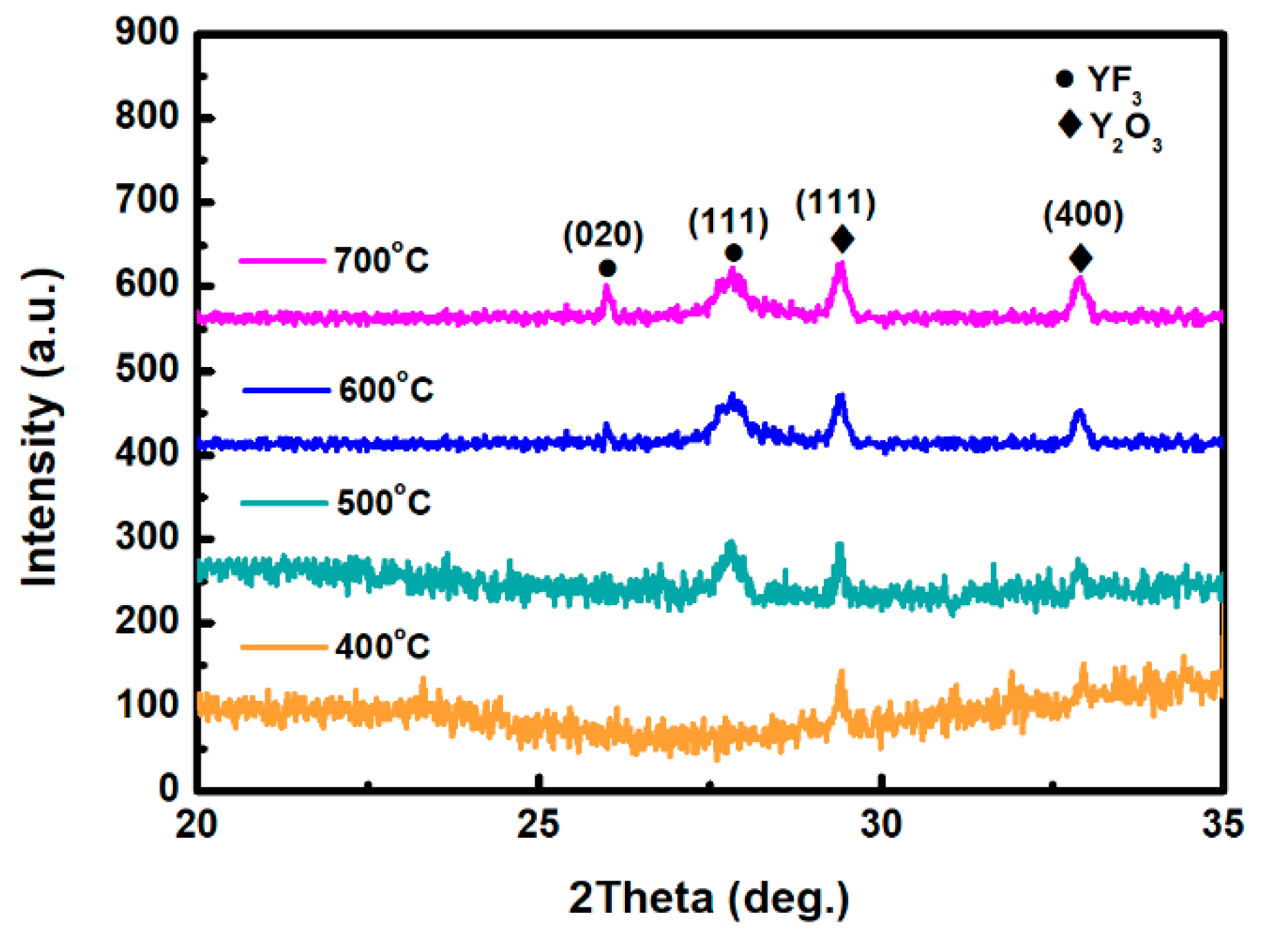
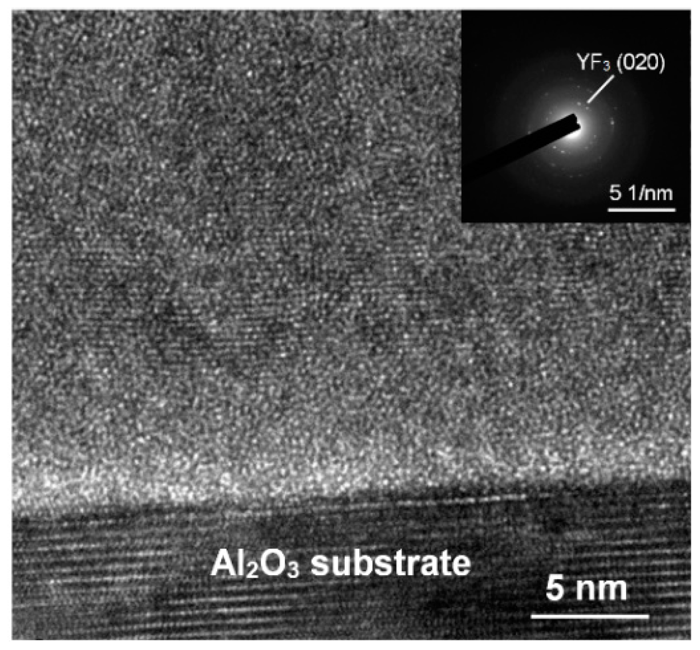
Figure 1 depicts the XRD scan patterns of YF3 films deposited on Al2O3 substrate at 400, 500, 600, and 700 °C. All YF3 samples were polycrystalline, and their structural orientations depended on the substrate temperature in the deposition process. The (020) plane of the orthorhombic YF3 phase was formed at substrate temperatures above 500 °C, which is in agreement with the reported data (JCPDS card files No. 74-0911) [11]. Moreover, the preferential orientation of the orthorhombic YF3 crystal structure differed in films fabricated at different temperatures. This might be attributed to the high kinetic energy imparted to YF3 molecules at high substrate temperatures, which enables them to migrate and rearrange on the substrate surface. YF3 samples fabricated at higher temperatures also showed a weak peak of the cubic Y2O3 phase (400) plane (JCPDS card files No. 79-1716), indicating contamination by oxygen atoms during the sputtering process [9]. As substrate temperature increases, Y2O3 formation might be favored by the higher instability of fluoride in the YF3 crystal lattice. Unstable F ions in the lattice can be gradually replaced by environmental oxygen atoms. Therefore, the number of oxygen atoms in the crystal lattice increases with increasing temperature, forming Y2O3 (see Figure 1). When YF3 film was deposited at a lower substrate temperature, an amorphous structure was formed. Amorphous film usually has a loose structure, resulting in greater thickness and a higher growth rate. In contrast, with increasing substrate temperature, the YF3 film became crystalline, and its crystal was relatively ordered. This indicates that a denser structure was found in the YF3 film grown at higher substrate temperatures, leading to its smaller thickness and lower growth rate. In TEM analysis, the YF3 films exhibited nanocrystalline grains with an average size of 5–20 nm (Figure 2). The regular ring-like electron diffraction pattern of a selected area (Figure 2, inset) implies a polycrystalline structure of YF3 film, consistent with the XRD result.
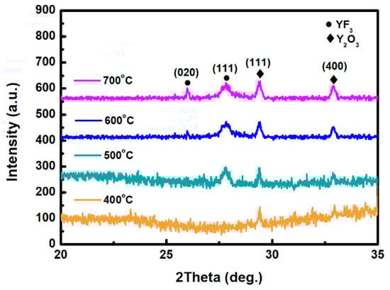
Figure 1.
XRD patterns of the as-deposited yttrium fluoride (YF3) films grown at 400, 500, 600, and 700 °C.

Figure 2.
TEM microstructure and selected area diffraction (inset) of YF3 film.
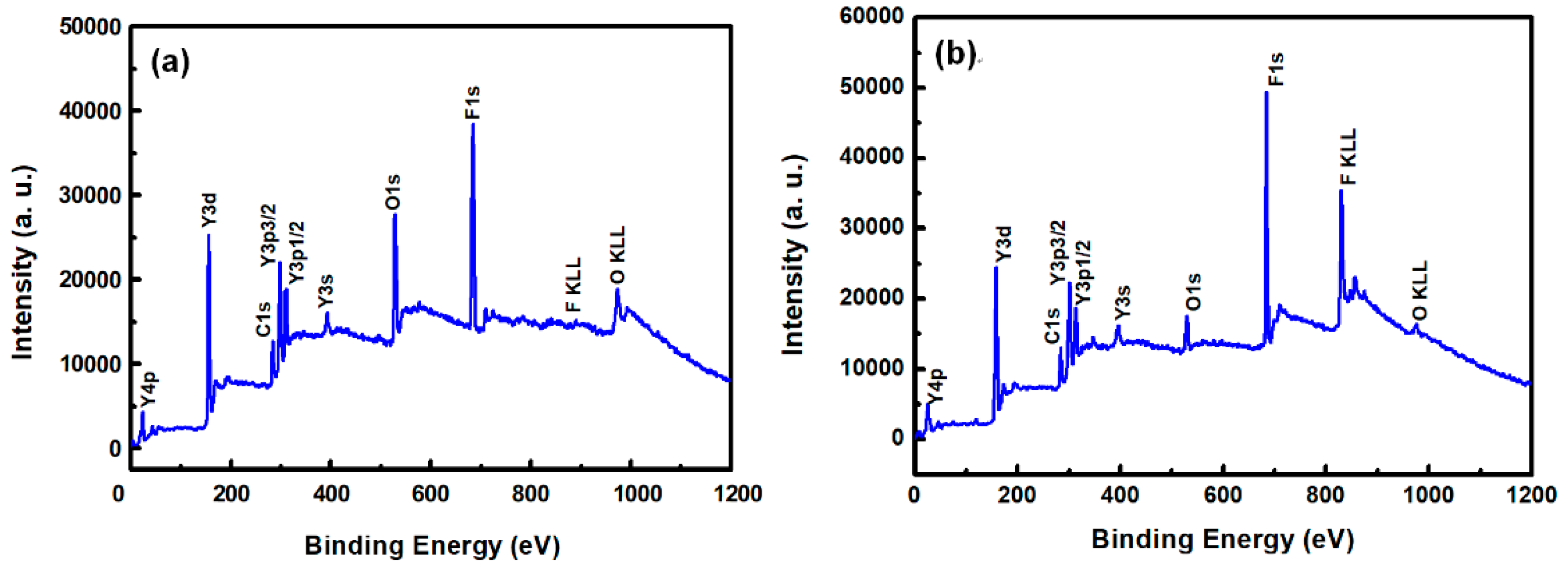
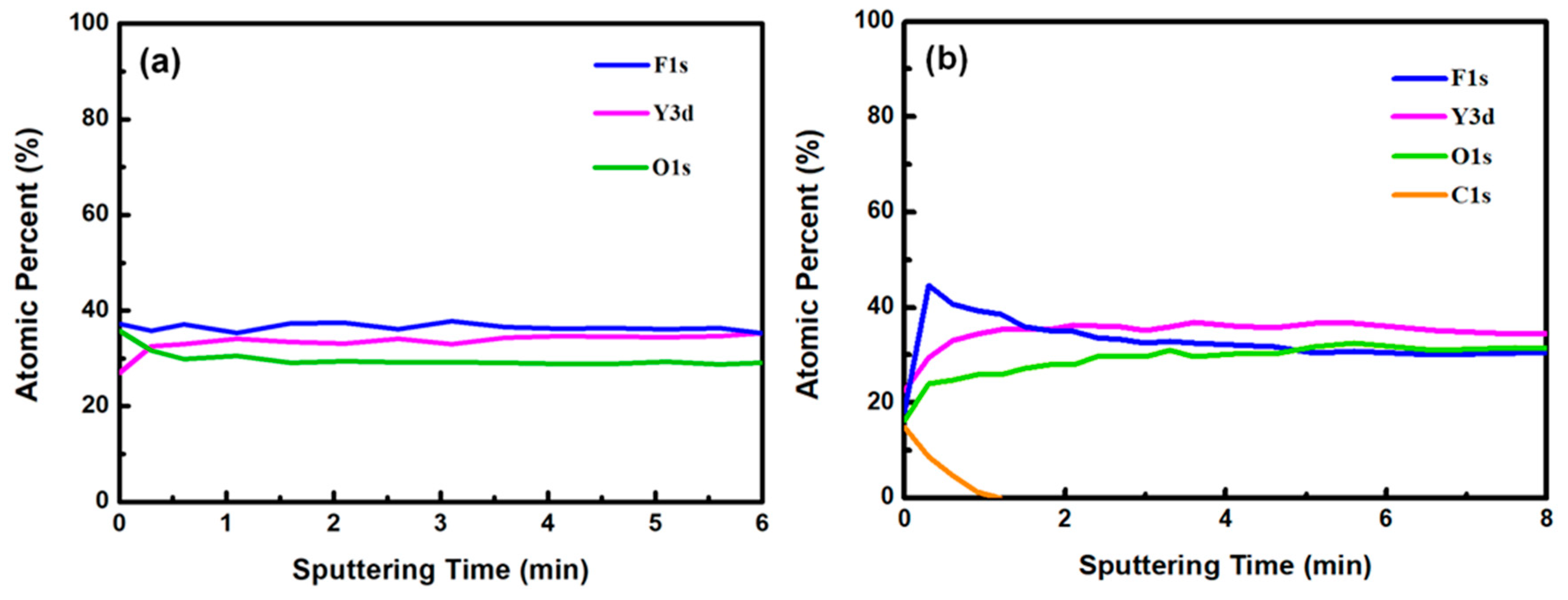
Figure 3a,b show the XPS survey spectra in the 0–1200 eV range of the YF3 films before and after CF4/O2 plasma etching, respectively. To collect the atomic signals, all samples were bombarded by argon ions for 2 min. The XPS peaks in the as-grown YF3 thin film (Figure 3a) correspond to Y, F, O, and C elements. The Y and F elements existed in the original YF3 film, and an O1s peak arose from oxygen contamination during the sputter deposition process. This result is consistent with previous reports [12]. After exposure to CF4/O2 plasma, the spectrum of the YF3 film exhibited an enhanced F1s peak and an additional C1s peak. The former feature is attributed to the high fluorine content of YF3, and the latter indicates the formation of a carbon-polymer surface layer under fluorocarbon plasma etching (Figure 3b). Figure 4a,b plot the compositions of the YF3 films as functions of sputtering time before and after exposure to the CF4/O2 plasma, respectively. Before exposure to the plasma, the maximum F content was 37% and the minimum O content was 32% (Figure 4a). This result indicates a two-phase mixture of YF3 and Y2O3 in the film, consistent with a previous study that reported a deficiency of fluorine atoms during the sputter deposition process [13]. The maximum percentage of F atoms in the etched sample was 44.69%, implying a fluorination layer on the YF3 specimen (Figure 4b). Similar results were observed in a previous study of surface fluorination by CF4/O2 plasma etching [14]. The carbon content on the YF3 surface decreased abruptly with sputtering time, indicating a very thin carbon polymer layer on the etched surface. This is because of interactions between the fluorocarbon plasma and Si-based materials, which generate carbon polymer and a SiFxOy reaction layer [15].
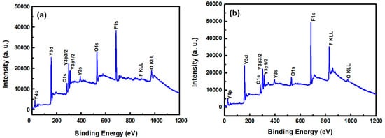
Figure 3.
XPS survey spectra of the surfaces of the YF3 thin films (a) before and (b) after exposure to CF4/O2 plasma (under bombardment with argon ions for two minutes).
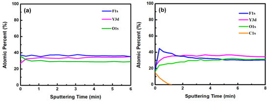
Figure 4.
Atomic percentages of YF3 film versus sputtering time (a) before and (b) after surface exposure to CF4/O2 plasma.
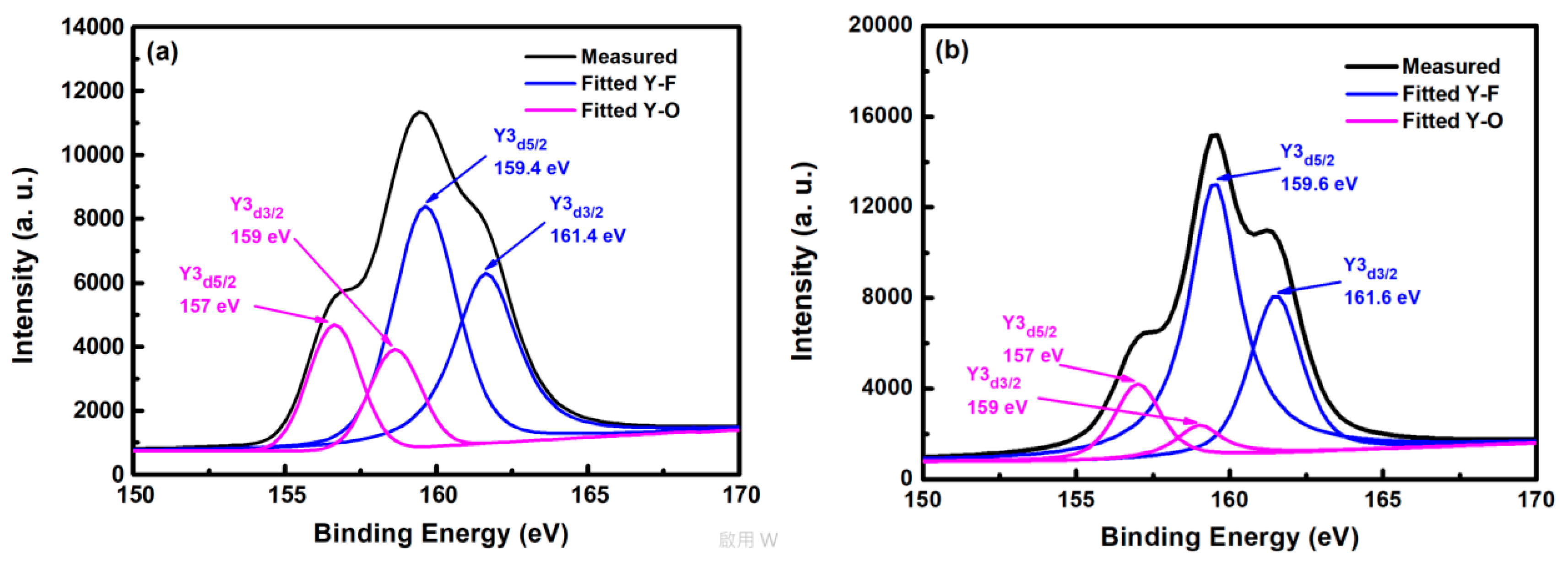
Figure 5 shows the XPS spectra of yttrium atoms of the YF3 film after CF4/O2 plasma etching. In the curve-fitted XPS spectra of the YF3 film, two peaks represent two bonding sources for Y cations, that is, the Y3d peak splits into a doublet (Y3d5/2 and Y3d3/2 electrons) with a binding-energy separation of 2 eV. The two yttrium bonding sources are consistent with the XPS standard [16]. The Y3d5/2 and Y3d3/2 peaks in the spectrum of the as-deposited YF3 film (Figure 5a) deconvolute into four peaks. The two peaks located at higher binding energies (159.4 and 161.4 eV) correspond to Y–F bonding in the YF3 film, whereas those at lower binding energies (157 and 159 eV) are ascribed to Y–O bonding. In the XPS spectra of etched YF3 film surface, the peaks are more intense than in the un-etched specimen (Figure 5b). Again, the strong doublet at higher binding energies (159.6 and 161.6 eV) and the weak doublet at lower binding energies (157 and 159 eV) correspond to Y–F and Y–O bonding, respectively. The higher XPS binding energy of the Y–F bonding can be attributed to the higher electronegativity of fluorine atoms (4.0) than oxygen atoms (3.5) [17]. Consequently, more electrons are transferred to fluorine, decreasing the electron density around the cation and enhancing the binding energy. Meanwhile, the intensity ratio of Y–F to Y–O bonds was estimated as 2.1 on etched YF3 films, indicating strong chemical interaction between the YF3 films and the fluorocarbon plasma.
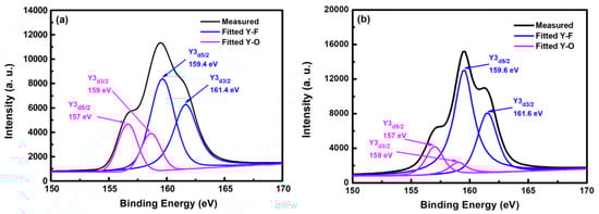
Figure 5.
X-ray photoelectron spectra of YF3 film (a) before and (b) after exposure to fluorocarbon plasma.
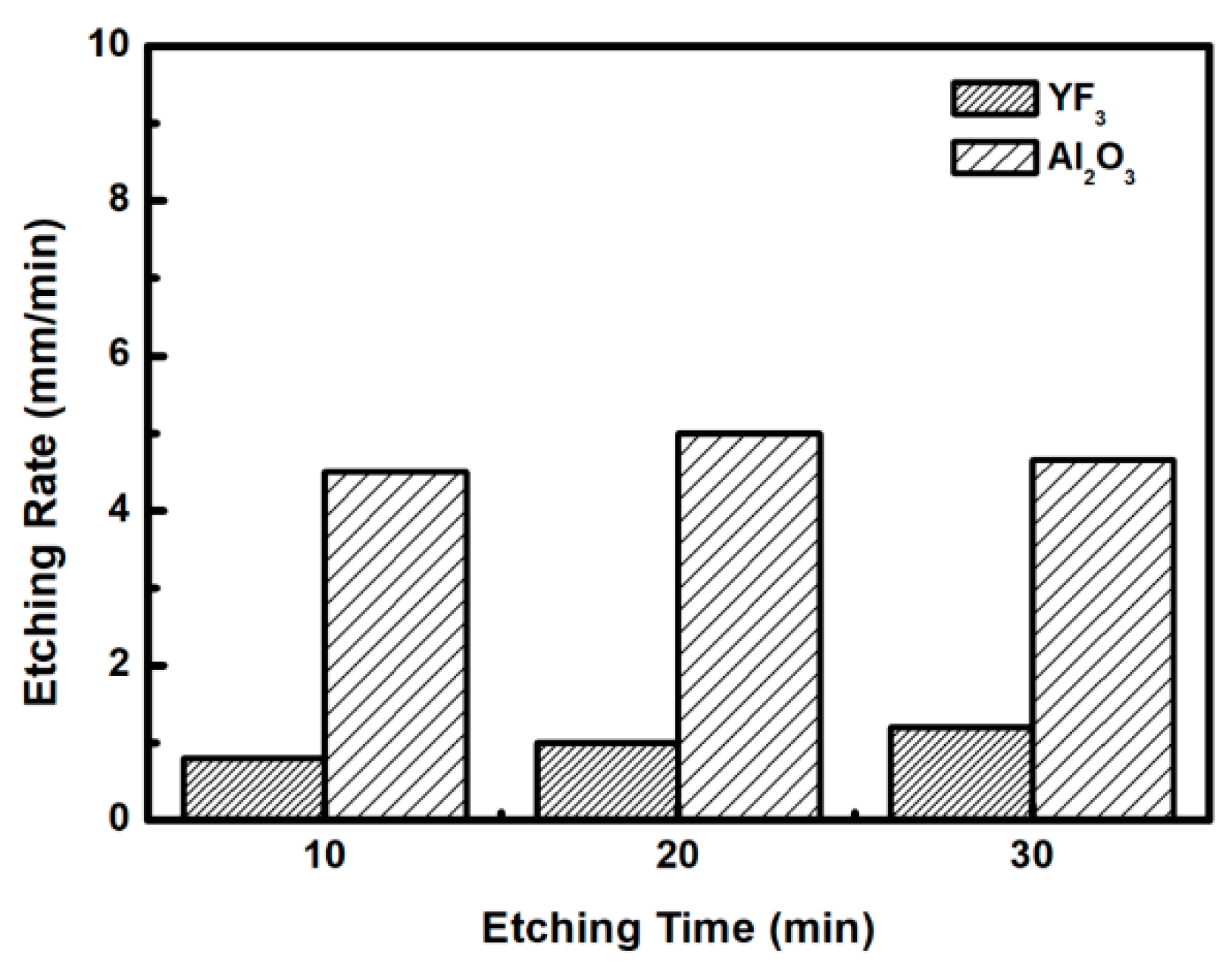
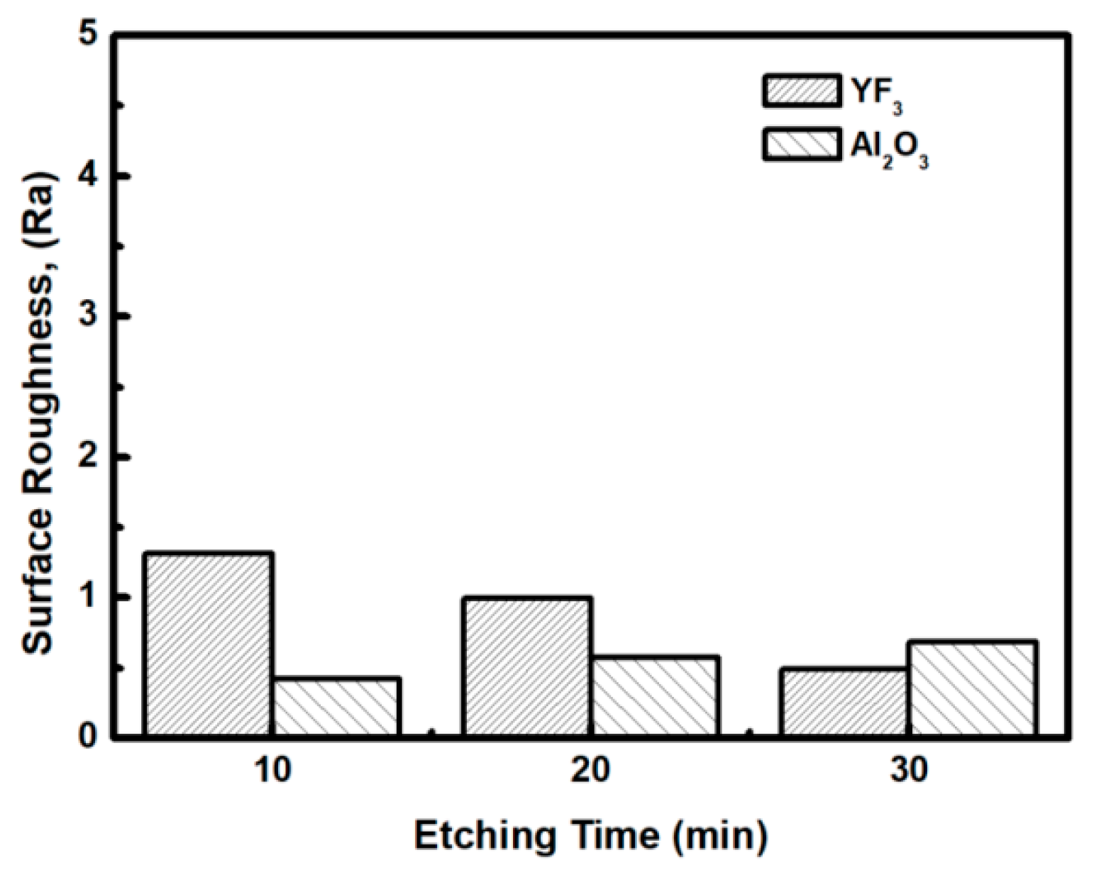
To evaluate the plasma erosion resistance of as-deposited YF3 films, the etching rate of the YF3-coated Al2O3 substrate was measured after exposure to the CF4/O2 plasma for different etching times. The etching rate of bare Al2O3 crystal was used as the reference. Figure 6 shows that the etching depths of both samples linearly increased with increasing etching time. After 30 min, the etching depth reached 120 mm in the sapphire, but only 38 mm in YF3. The erosion resistance of the YF3 film to CF4/O2 plasma etching was more than three times higher than that of sapphire crystal. This is attributed to the chemical stability of YF3 in a chemical environment dominated by fluorocarbon plasma. The surface morphologies and roughness of the YF3 films etched for different lengths of time were measured by AFM measurements, with a scanning area of 5 m2. The surface roughness results are shown in Figure 7. The etching time of the CF4/O2 plasma did not remarkably influence the surface roughness of the YF3 film.
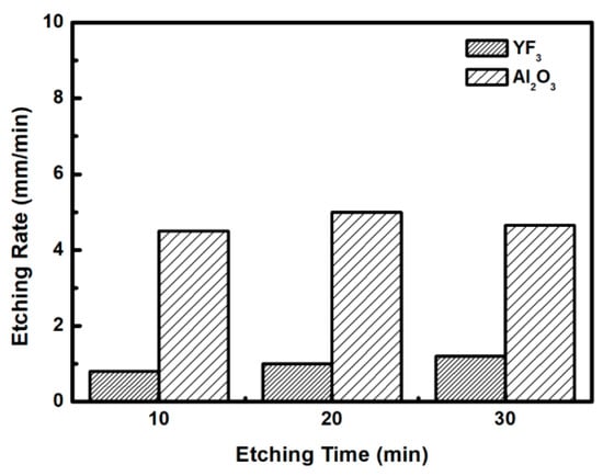
Figure 6.
Etching depths of the YF3 film and Al2O3 substrates after different CF4/O2 plasma exposure times.
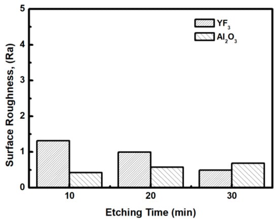
Figure 7.
Surface roughness of YF3 and Al2O3 exposed to fluorocarbon plasma for different etching times.
Figure 8a,b show the surface microstructures of YF3 and Al2O3 samples, respectively, after the etching experiment. The micrographs were acquired by optical microscopy (OM). The right and left images in each panel show the un-etched and etched surfaces, respectively. The step height of the Al2O3 sample changed after CF4/O2 plasma etching. These images confirm the hardness and stronger CF4/O2 corrosion resistance of the YF3 films compared to conventional Al2O3 substrate.
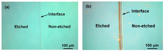
Figure 8.
Optical micrographs of the (a) YF3 and (b) Al2O3 substrates after exposure to fluorocarbon plasma.
AlF3 is a typical fluoride of Al2O3 materials [4]. The boiling temperature of YF3 (2230 °C) is higher than the sublimation temperature of AlF3 (1275 °C). Hence, YF3 is more stable and more difficult to vaporize than AlF3. Therefore, its fluorinated layer can be removed by a physical sputtering process. The sputtering yields of the films are inversely proportional to sublimation enthalpies of their compounds [18]. The sublimation enthalpy of YF3 (481 ± 21 kJ/mol) is higher than that of AlF3 (301 ± 4 kJ/mol). Moreover, the enthalpy of formation of the metal–oxygen bond is lower in YF3 (−392 kJ mol−1) than in Al2O3 (−279 kJ mol−1). Therefore, YF3 is chemically more stable than Al2O3 [19]. In particular, YF3 is extremely stable under the fluorocarbon plasma etching process.
Figure 9 shows a cross-sectional HRTEM image of the YF3 film after CF4/O2 plasma exposure. Continuous and nearly-complete lattice fringes were observed near the surface, indicating that the YF3 ceramic crystalline lattice was not distorted by the fluorine plasma irradiation. Furthermore, the d-spacings of the near surface of film were 3.131 Å (blue dotted circle) and 2.621 Å (red dotted circle), very close to the d-spacings of the altered layers of yttrium oxyflouride (YOF): 3.147 Å (006) and 2.698 Å (104) [11]. The thin YOF layer formed on the YF3 surface plays a protective role, suppressing the particle generation during CF4/O2 plasma etching process. The reaction and formation of an altered YOF layer has been reported previously [14]. Therefore, YF3 film is a very attractive plasma-corrosion-resistant material that produces fewer contamination particles during the semiconductor fabrication process.
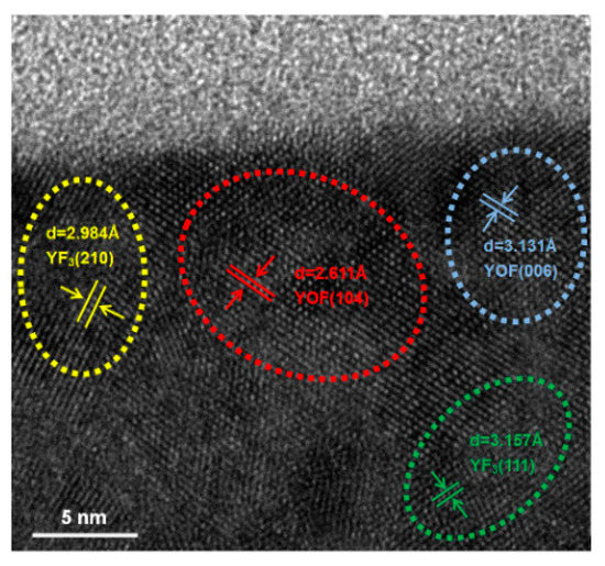
Figure 9.
Cross-sectional high-resolution transmission electron microscopy (HRTEM) image of the YF3 film after exposure to fluorine plasma.
4. Conclusions
YF3 films were successfully deposited through radio frequency magnetron sputtering on sapphire substrates at different temperatures. HRTEM and XRD results revealed polycrystalline YF3 films with an orthorhombic structure. XPS results confirmed the superior chemical stability of YF3 film after fluorocarbon plasma treatment. The robustness of YF3 film was confirmed to be more than that of Al2O3 film after the plasma exposure. The YF3 film is expected to provide a more protective barrier than Al2O3 or quartz plates in the fluorine plasma etching process.
Author Contributions
Conceptualization: W.-K.W.; Methodology: Y.-X.L., Y.-J.S. and W.-K.W.; Data curation: Y.-X.L., Y.-J.S. and W.-K.W.; Writing—original draft preparation: Y.-X.L., Y.-J.S. and W.-K.W.; Writing—review and editing: W.-K.W.
Funding
This research was funded by the Ministry of Science and Technology of Taiwan (No. 107-2221-E-212-004).
Acknowledgments
The authors wish to express their sincere gratitude for the technical support from the Advanced Industry Technology Centre of National Chung Hsing University, Taiwan.
Conflicts of Interest
The authors declare no conflict of interest.
References
- Kim, D.M.; Kim, K.B.; Yoon, S.Y.; Oh, S.Y.; Kim, H.T.; Lee, S.M. Effects of artificial pores and purity on the erosion behaviors of polycrystalline Al2O3 ceramics under fluorine plasma. J. Ceram. Soc. 2009, 117, 863–867. [Google Scholar] [CrossRef]
- Zavareh, M.A.; Sarhen, A.A.D.M.; Razak, B.B.; Basirun, W.J. Plasma thermal spray of ceramic oxide coatingon carbon steel with enhanced wear and corrosion resistance for oil and gas applications. Ceram. Int. 2014, 40, 14267–14277. [Google Scholar] [CrossRef]
- Fukumoto, H.; Fujikake, I.; Takao, Y.; Eriguchi, K.; Ono, K. Plasma chemical behavior of reactants and reaction products during inductively coupled CF4 plasma etching of SiO2. Plasma Sources Sci. Technol. 2009, 18, 045027. [Google Scholar] [CrossRef]
- Kitamura, T.; Mizuno, H.; Kato, N.; Aoki, I. Plasma-erosion properties of ceramic coating prepared by plasma spraying. Mater. Trans. 2006, 47, 1677–1683. [Google Scholar] [CrossRef]
- Duc, L.M.; Tan, C.M.; Luo, M.; Leng, I.C.H. Maintenance scheduling of plasma etching chamber in wafer fabrication for high-yield etching process. IEEE Trans. Semicond. Manuf. 2014, 27, 204–211. [Google Scholar] [CrossRef]
- Iwasawa, J.; Nishimizu, R.; Tokita, M.; Kiyohara, M.; Uematsu, K. Plasma-resistant dense yttrium oxide film prepared by aerosol deposition process. J. Am. Ceram. Soc. 2007, 90, 2327–2332. [Google Scholar] [CrossRef]
- Mun, S.Y.; Shin, K.C.; Lee, S.S.; Kwak, J.S.; Jeong, J.Y.; Jeong, Y.H. Etch defect reduction using SF6/O2 plasma cleaning and optimizing etching recipe in photo resist masked gate poly silicon etch process. Jpn. J. Appl. Phys. 2005, 44, 4891–4895. [Google Scholar] [CrossRef]
- Kim, D.M.; Oh, Y.S.; Kim, S.; Kim, H.T.; Lim, D.S.; Lee, S.M. The erosion behaviors of Y2O3 and YF3 coatings under fluorocarbon plasma. Thin Solid Films 2011, 519, 6698–6702. [Google Scholar] [CrossRef]
- Lin, T.K.; Wuu, D.S.; Huang, S.Y.; Wang, W.K. Characteristics of yttrium fluoride and yttrium oxide coatings for plasma process equipment prepared by atmospheric plasma spraying. Jpn. J. Appl. Phys. 2016, 55, 126201. [Google Scholar] [CrossRef]
- Chakravarthy, Y.; Bhandari, S.; Chaturvedi, V.; Pragatheeswaran, A.; Nagraj, A.; Thiyagarajan, T.K.; Ananthapadmanaban, P.V.; Das, A.K. Plasma spray deposition of yttrium oxide on graphite, coating characterization and interaction with molten uranium. J. Eur. Ceram. Soc. 2015, 35, 781–794. [Google Scholar] [CrossRef]
- Chai, G.D.; Dong, G.P.; Qiu, J.R.; Zhang, Q.Y.; Yang, Z.M. Phase transformation and intense 2.7 mm emission from Er3+ oped YF3/YOF submicron-crystals. Sci. Rep. 2013, 3, 1598. [Google Scholar] [CrossRef] [PubMed]
- Pei, L.; Jiapi, Z.; Yuankun, Z.; Jiecai, H. Preparation and optical properties of sputtered-deposition yttrium fluoride film. Nucl. Instrum. Methods Phys. Res. Sect. B 2013, 307, 429–433. [Google Scholar] [CrossRef]
- Quesnel, E.; Berger, M.; Duca, D.; Pelle, C.; Pierre, F. Near-UV to IR optical characterization of YF3 thin films deposited by evaporation and ion beam processes. Proc. SPIE 1996, 2776, 366–372. [Google Scholar]
- Lin, T.K.; Wang, W.K.; Huang, S.Y.; Tasi, C.T.; Wuu, D.S. Comparison of erosion behavior and particle contamination in mass-production CF4/O2 plasma chambers using Y2O3 and YF3 protective coatings. Nanomaterials 2017, 7, 183. [Google Scholar] [CrossRef] [PubMed]
- Matsui, M.; Tatsumi, T.; Sekine, M. Observation of surface reaction layers formed in highly selective SiO2 etching. J. Vac. Sci. Technol. 2001, 19, 1282–1888. [Google Scholar] [CrossRef]
- Moulder, J.F.; Stickle, W.F.; Sobol, P.E.; Bomben, K.D. Handbook of X-ray Photoelectron Spectroscopy; Physical Electronics: Eden Prairie, MN, USA, 1995; p. 10. [Google Scholar]
- Zhong, H.X.; Hong, J.M.; Cao, X.F.; Chen, X.T.; Xue, Z.L. Ionic-liquid-assisted synthesis of YF3 with different crystalline phases and morphologies. Mater. Res. Bull. 2009, 44, 623–628. [Google Scholar] [CrossRef]
- Cao, Y.C.; Zhao, L.; Luo, J.; Wang, K.; Zhang, B.P.; Yokota, H.; Ito, Y.; Li, J.F. Plasma etching behavior of Y2O3 ceramics: Comparative study with Al2O3. Appl. Surf. Sci. 2016, 366, 304–309. [Google Scholar] [CrossRef]
- Brunetti, B.; Piacente, V.; Scardala, P. Torsion vapor pressure and sublimation enthalpies of aluminum trifluoride and aluminum trichloride. J. Chem. Eng. Data 2009, 54, 940–944. [Google Scholar] [CrossRef]


© 2018 by the authors. Licensee MDPI, Basel, Switzerland. This article is an open access article distributed under the terms and conditions of the Creative Commons Attribution (CC BY) license (http://creativecommons.org/licenses/by/4.0/).