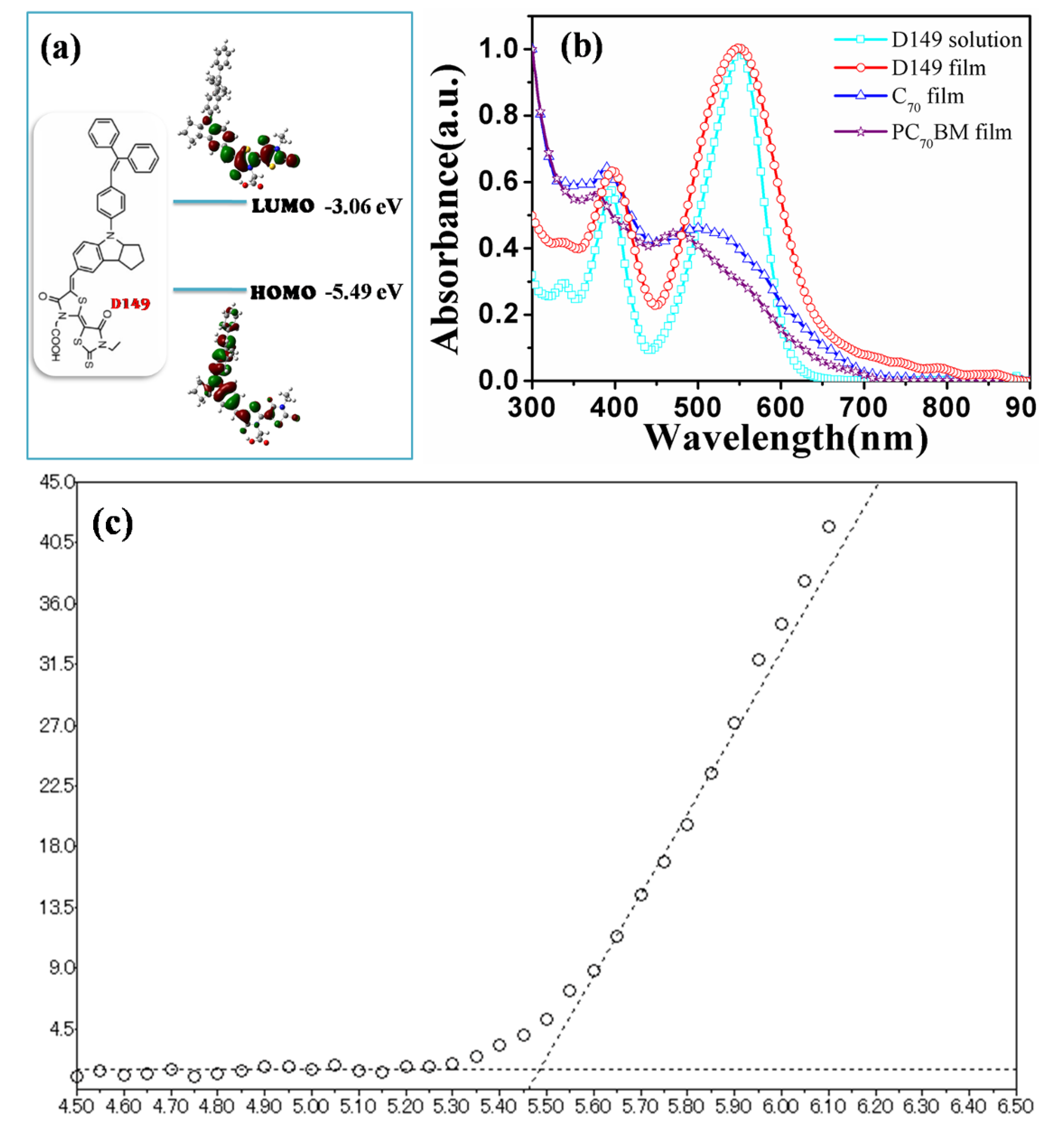
2.1. Molecular Structure
The molecular structure of D149 is shown in
Figure 1a. D149 consists of a D-A structure, in which the indoline unit acts as an electron-donating moiety and the carboxyl-functionalized double rhodanine rings act as electron-withdrawing moieties.
Figure 1a also shows the calculated HOMO and LUMO of D149 by density functional theory (DFT), together with the energy levels obtained from UV photoelectron spectroscopy. The Photoelectron Yield Spectrometer AC-3 setup was utilized to measure the HOMO level of D149. The HOMO energy level of D149 measured in thin solid film by AC-3 is −5.49 eV (
Figure 1c). The LUMO energy level of D149 was calculated to be −3.06 eV from the measured HOMO level and the optical band-gap (2.43 eV) of D149 from its UV-Vis absorption spectrum. As a result of the D-A architecture of D149, intramolecular charge-transfer (ICT) could take place [
22]. The electrons move from the indoline moiety in the highest occupied molecular orbital (HOMO) to the rhodanine moiety in the lowest unoccupied molecular orbital (LUMO). The HOMO level of D149 is deep enough for a build-in potential with a fullerene-type electron acceptor, while the LUMO level is high enough for efficient interfacial charge transfer to PC
70BM.
Figure 1.
(a) Molecular structure and molecular orbitals of D149; (b) Normalized Absorption spectra of D149 in solid film and solution, and C70 and PC70BM in solid films; (c) The HOMO level of D149 measured by AC-3 was −5.49 eV.
Figure 1.
(a) Molecular structure and molecular orbitals of D149; (b) Normalized Absorption spectra of D149 in solid film and solution, and C70 and PC70BM in solid films; (c) The HOMO level of D149 measured by AC-3 was −5.49 eV.
Figure 1b shows the normalized ultraviolet-visible (UV-Vis) absorption spectra of D149 dye in CHCl
3 solution and spin-cast as a thin solid film, and compared to the absorption spectrum of C
70 and PC
70BM films. The broader absorption peaks of D149 in the thin solid film than in solution could be attributed to aggregate formation as a result of fast solvent evaporation, although this is not as serious as in DSCs. It has been found that D149 is more soluble in CHCl
3 than in other typical OSC solvents. All subsequent characterizations and solar cell device fabrications were therefore carried out using CHCl
3 solutions of D149. The absorption spectra for the donor D149 and the acceptor C
70 and PC
70BM are quite similar in the absorption region, but with differences in the density of each absorption peak.
2.2. BHJ Solar Cells Based on a D149/PC70BM
In order to produce a large interface between the donor and acceptor molecules, solution-processed bulk-heterojunction (BHJ) devices based on a D149/PC
70BM active layer were fabricated first.
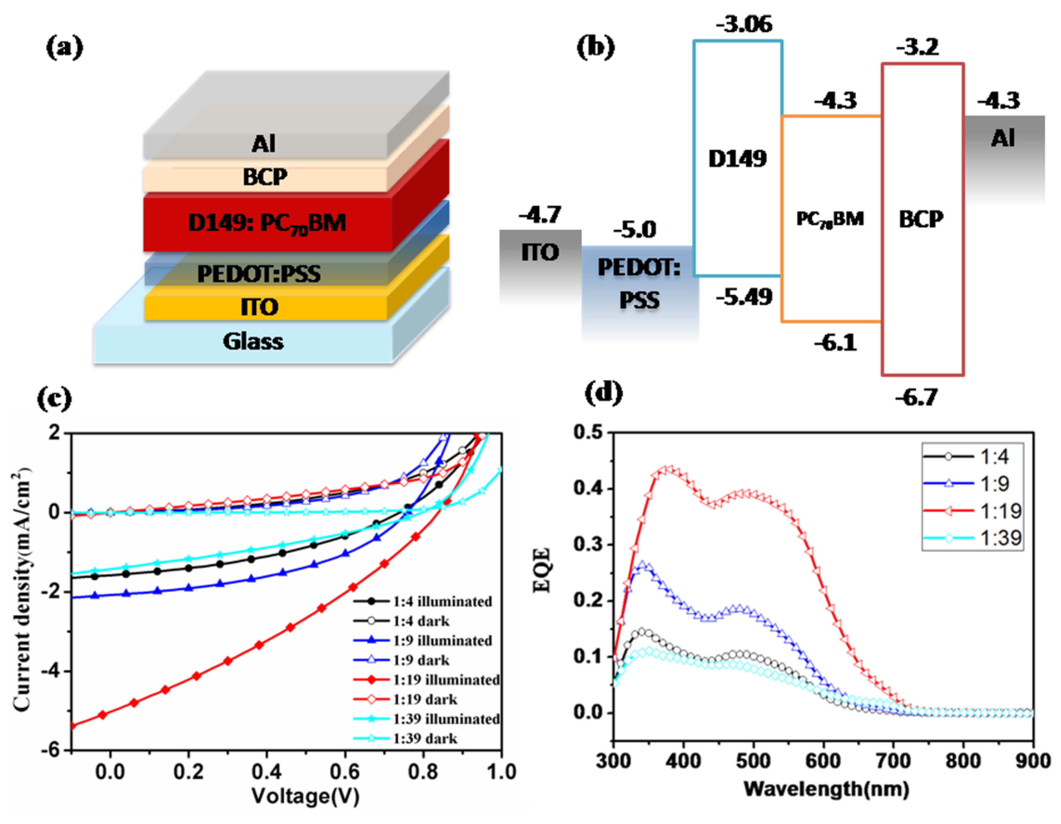
Figure 2a shows the device structure,
i.e., ITO/PEDOT: PSS (40 nm)/D149:PC
70BM/BCP (10 nm)/Al (100 nm). PEDOT: PSS acts as a hole-transporting layer and BCP acts as an exciton-blocking layer. The active layer was prepared by spin-coating CHCl
3 solutions containing 1 mg·mL
−1 of D149 with different amounts of PC
70BM, to give a final D149 concentration of 2.5–20 wt% in the blend film.
Figure 2b shows the energy level alignment of different materials in the BHJ solar cells. Both the HOMO (−5.49 eV) and LUMO level (−3.06 eV) of D149 are above that of PC
70BM, indicating that hot-electron transport from D149 to PC
70BM is favorable.
Figure 2.
(a) Device architecture of BHJ solar cell, ITO/PEDOT: PSS/D149: PC70BM/BCP/Al; (b) Energy level alignment within the BHJ device; (c) J-V curves of the BHJ solar cell with different blending ratios (w/w) of D149: PC70BM; (d) EQE spectra of the corresponding BHJ devices.
Figure 2.
(a) Device architecture of BHJ solar cell, ITO/PEDOT: PSS/D149: PC70BM/BCP/Al; (b) Energy level alignment within the BHJ device; (c) J-V curves of the BHJ solar cell with different blending ratios (w/w) of D149: PC70BM; (d) EQE spectra of the corresponding BHJ devices.
Figure 2c,d shows the current density-voltage (
J-V) curves and external quantum efficiencies (EQE) spectra of the BHJ cells based on different D149/PC
70BM blending ratios.
Table 1 lists the relevant parameters extracted from the
J-V curves. Interestingly, the best PCE obtained for such a BHJ device was 1.29%,with a
Voc of 0.90 V, a
Jsc of 4.58 mA·cm
−2, and a FF of 0.31, for D149/PC
70BM with a blending ratio as low as 1:19 (5% weight content of D149). This suggests that a low concentration of donor molecules in the blend film may play a different role in such a cell from that in other BHJ OPVs. Similar phenomena have already been observed for thermally evaporated BHJ devices, in which concentrations of donor molecules as low as 5% gave the highest PV performance. The mechanism has been partially attributed to Schottky barrier contact between the donor and MoOx layers [
23], however, this is obviously not the case in our system, since replacing PEDOT:PSS with MoO
3 gave a slightly lower PCE of 1.02%, with a
Voc of 0.90 V, a
Jsc of 3.72 mA·cm
−2, and an FF of 0.31. The difference in PCE originated mainly from the different
Jsc values of the two devices. The HOMO level of D149 is higher than the work function of MoO
3 (−5.50 eV), and lower than the work function of PEDOT: PSS (−5.00 eV). Hole injection from D149 to PEDOT: PSS will therefore be more effective than that to MoO
3, which would result in a higher
Jsc of the device. On the other hand, the relatively low FF of both devices might be attributed to poor charge-transport within the active layers. The high polarity of the D149 dye not only causes the low solubility of the dye in organic solvents, but also reduces the charge mobility of the molecule and the resultant carrier-transport in blend films. In order to achieve better PV performances, it is important to overcome the issue of the low carrier-mobility of the D149 donor molecule in OPV devices. Fabrication of a bilayer-heterojunction device with a relatively thin layer of D149 is therefore preferable, since charge transport in such a device might be less affected by the charge-carrier mobility.
Table 1.
Performance details of the photovoltaic devices sharing a structure of ITO/PEDOT: PSS/D149:PC70BM/BCP/Al, varying the blending ratios (w/w) of D149: PC70BM from 1:4 to 1:39, under AM 1.5G 100 mW·cm−2 illumination.
Table 1.
Performance details of the photovoltaic devices sharing a structure of ITO/PEDOT: PSS/D149:PC70BM/BCP/Al, varying the blending ratios (w/w) of D149: PC70BM from 1:4 to 1:39, under AM 1.5G 100 mW·cm−2 illumination.
| Blending ratio (w/w) of D149:PC70BM | Jsc (mA/cm2) | Voc (V) | FF | PCE (%) |
| 1:4 | 1.58 | 0.74 | 0.39 | 0.45 |
| 1:9 | 2.08 | 0.76 | 0.44 | 0.69 |
| 1:19 | 4.58 | 0.90 | 0.31 | 1.29 |
| 1:39 | 1.42 | 0.80 | 0.32 | 0.36 |
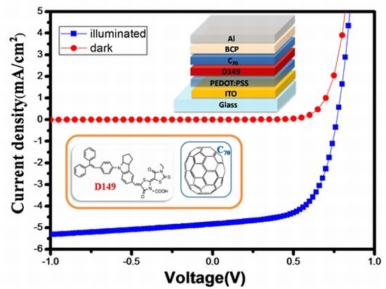
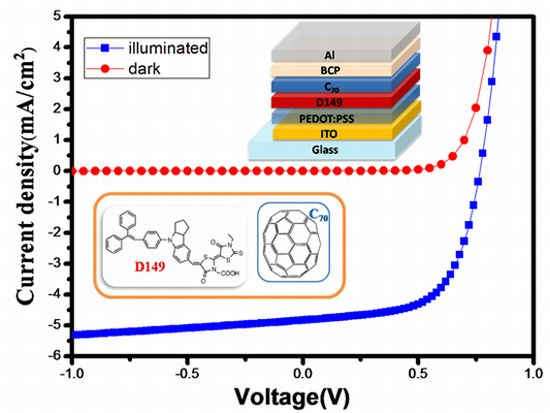
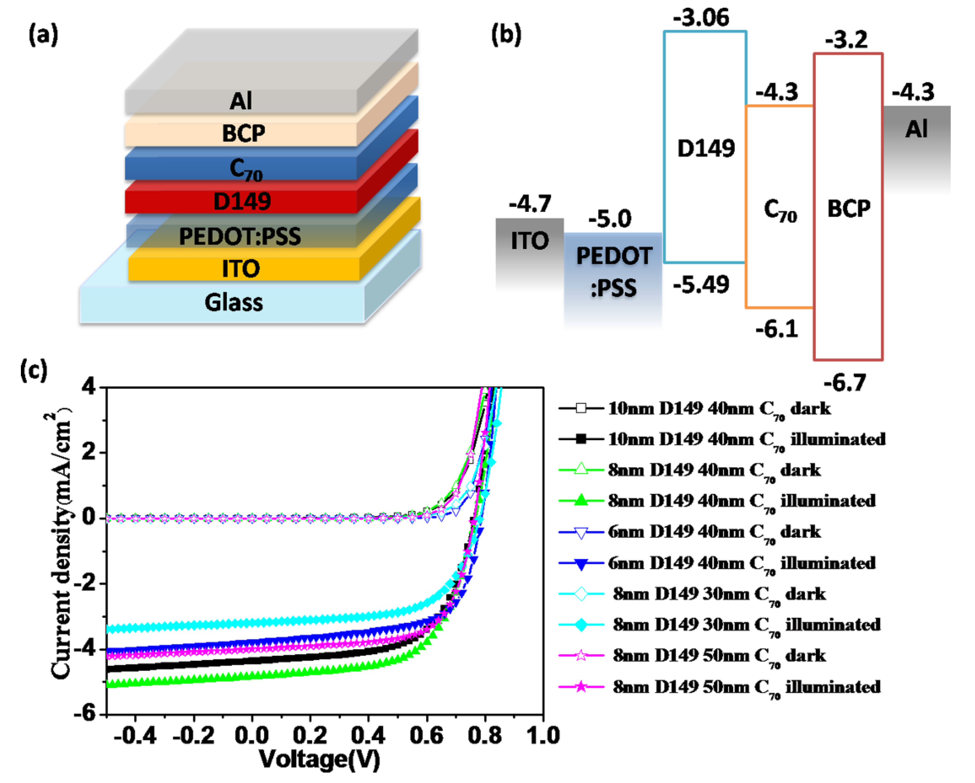
2.3. Bilayer-Heterojunction Solar Cells based on a D149/C70
Figure 3a shows a bilayer-heterojunction PV device with the structure ITO/PEDOT:PSS (30 nm)/D149/C
70 (40 nm)/BCP (10 nm)/Al (100 nm), and
Figure 3b shows the energy alignment of each layer. D149 layers of 6–10 nm thickness were obtained by spin-coating a 1 mg·mL
−1 D149 CHCl
3 solution on top of the PEDOT: PSS layer. The best PV performance for this bilayer structure was 2.28% for a PCE calculated from a
Voc of 0.77 V, a
Jsc of 4.83 mA·cm
−2, and an FF of 0.62, using an 8 nm-thick D149 layer. The PV performance decreases for both thinner and thicker D149 layers, as shown in
Table 2. More specifically, the PCE of the reference device with a 10 nm-thick D149 layer was 2.06%, with a
Voc of 0.76 V, a
Jsc of 4.36 mA·cm
−2, and an FF of 0.62, whereas a PCE of 1.93%, with a
Voc of 0.78 V, a
Jsc of 3.83 mA·cm
−2, and an FF of 0.65 was obtained for a device based on a 6 nm-thick D149 layer. In the best BHJ device described above, the enhanced values of
Jsc and FF for the bilayer structure device could both be attributed to facilitated hole-transport in such a thin film of D149, since the thickness of the D149 layer is within the resonance energy transfer distance. Obviously, the reduced PV performance with increased film thickness from 8 nm to 10 nm also supports the above theory, especially for donor molecules with relatively low carrier-mobility. On the other hand, the decreased PV performance with decreased film thickness from 8 nm to 6 nm was mainly the result of reduced photocurrent generation, originating from the low light-harvesting capabilities of such OPV devices. The better photovoltaic performance of D149 in bilayer-heterojunction devices than in BHJ devices was due to its very high light absorption coefficients so that 8–10 nm thick dye layer can capture most of the visible light, maintaining the effective hole transportation within such a thin layer at the same time.
Figure 3.
(a) Device architecture of bilayer devices; (b) Energy level alignment within the devices; (c) J-V curves of the bilayer devices with different thickness of D149 and C70.
Figure 3.
(a) Device architecture of bilayer devices; (b) Energy level alignment within the devices; (c) J-V curves of the bilayer devices with different thickness of D149 and C70.
Table 2.
Performance details of the photovoltaic devices sharing a structure of ITO/PEDOT: PSS/D149/C70/BCP/Al, varying the thickness of D149 from 6 nm to 10 nm and the thickness of C70 from 30 nm to 50 nm, under AM 1.5G 100 mW·cm−2 illumination.
Table 2.
Performance details of the photovoltaic devices sharing a structure of ITO/PEDOT: PSS/D149/C70/BCP/Al, varying the thickness of D149 from 6 nm to 10 nm and the thickness of C70 from 30 nm to 50 nm, under AM 1.5G 100 mW·cm−2 illumination.
| Layer thickness | Jsc (mA/cm2) | Voc (V) | FF | PCE (%) |
|---|
| D149 6 nm C70 40 nm | 3.83 | 0.78 | 0.65 | 1.93 |
| D149 8 nm C70 40 nm | 4.83 | 0.77 | 0.62 | 2.28 |
| D149 10 nm C70 40 nm | 4.36 | 0.76 | 0.62 | 2.06 |
| D149 8 nm C70 30 nm | 3.19 | 0.78 | 0.62 | 1.55 |
| D149 8 nm C70 50 nm | 4.00 | 0.76 | 0.67 | 2.04 |
Similarly, the thickness of the C70 layer has also been optimized for OPV devices with an 8 nm-thick D149 layer. The device with a 30 nm-thick C70 layer gave a PCE of 1.55%, with a Voc of 0.78 V, a Jsc of 3.19 mA·cm−2, and an FF of 0.62. The device with a 50 nm-thick C70 layer had a PCE of 2.04%, with a Voc of 0.76 V, a Jsc of 4.00 mA·cm−2, and an FF of 0.67. The changes in PV performance for different C70 thicknesses are caused mainly by changes in the photocurrent. The C70 thickness was changed in steps of 10 nm, and this could cause large differences in the optical effects within the device and in photon capture within the active layer.
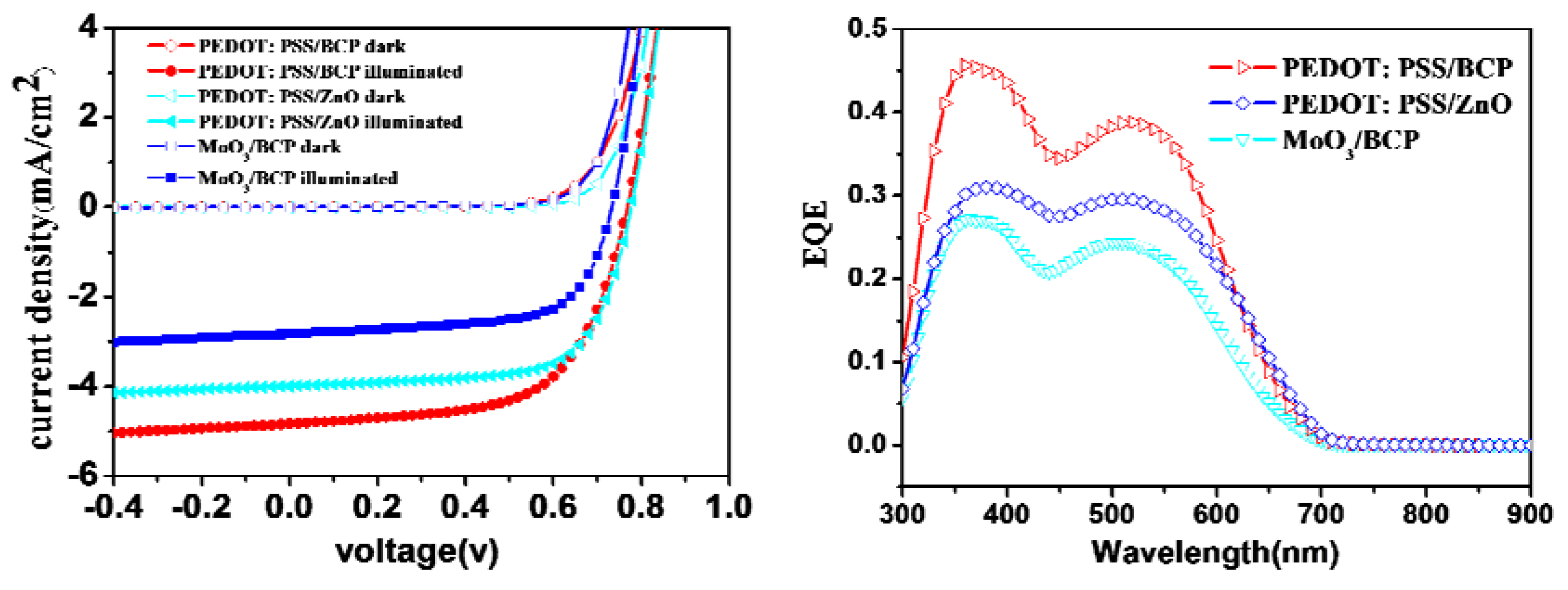
The electron- and hole-transport layers on both sides of the bilayer device are another important issue in determining the PV performances of such OPVs. We chose ZnO and MoO
3 as alternatives to BCP and PEDOT: PSS for the electron- or hole-transport layers.
Figure 4 shows the
J-V curves and external quantum efficiency (EQE) spectra of OPV devices based on different electron- and hole-transport layers.
Table 3 lists detailed parameters extracted from the
J-V curves. Unlike the BCP layer, which was evaporated onto the C
70 layer, the ZnO layer was spin-coated from a ZnO nanoparticle suspension. A 40 nm-thick C
70 layer in the best OPV device was found to be insufficient to protect the D149 under-layer from a ZnO/butanol solution. A 50 nm-thick C
70 layer was therefore used instead. Actually, there has been none of example of using ZnO as the electron transport layer for the bilayer-heterojunction OSC devices, since transferring samples out of vacuum chamber before depositing metal electrode usually causes very bad PV performance. Therefore, the success of using solution processed ZnO electron transport layer in the present study newly provided a useful tool for improving the PV performance of thermal evaporated OSC devices. The OSC device based on a solar cell configuration of ITO/PEDOT:PSS (40 nm)/D149/C
70 (50 nm)/ZnO (10 nm)/Al (100 nm) gave a PCE of 2.10%, with a
Voc of 0.78 V, a
Jsc of 3.99 mA·cm
−2, and an FF of 0.68; this was slightly worse than the PCE of a PEDOT:PSS/BCP-based OPV device with a 40-nm-thick C
70 layer, but better than that with a 50-nm-thick C
70 layer. The high FF in the ZnO-based device could be attributed to the excellent electron-mobility of ZnO, which reduces the device resistance. In contrast, the photocurrent and solar cell performance were substantially lowered by replacing PEDOT: PSS with MoO
3. This might be caused by a poorer interface between the MoO
3 and D149 layers. Moreover, the fact that the
Jsc values in the
J-V curves are in good agreement with the integrated area under the external quantum efficiency profiles strongly supports our statement above.
Figure 4.
J-V curves and EQE profiles of devices based on a structure of ITO/Hole transport layer/D149 (8 nm)/C70 (40 or 50 nm)/Electron transport layer/Al (100 nm) with different electron- and hole-transport layers under AM 1.5G illumination or dark conditions.
Figure 4.
J-V curves and EQE profiles of devices based on a structure of ITO/Hole transport layer/D149 (8 nm)/C70 (40 or 50 nm)/Electron transport layer/Al (100 nm) with different electron- and hole-transport layers under AM 1.5G illumination or dark conditions.
Table 3.
Photovoltaic performances of D149 based bilayer OPV devices based on a structure of ITO/Hole transport layer/D149 (8 nm)/C70/Electron transport layer/Al using different electron- and hole-transport layers.
Table 3.
Photovoltaic performances of D149 based bilayer OPV devices based on a structure of ITO/Hole transport layer/D149 (8 nm)/C70/Electron transport layer/Al using different electron- and hole-transport layers.
| Hole/Electron transport layer | Jsc (mA/cm2) | Voc (V) | FF | PCE (%) |
|---|
| PEDOT: PSS/BCP | 4.83 | 0.77 | 0.62 | 2.28 |
| PEDOT: PSS/ZnO | 3.99 | 0.78 | 0.68 | 2.10 |
| MoO3/BCP | 2.83 | 0.73 | 0.65 | 1.36 |
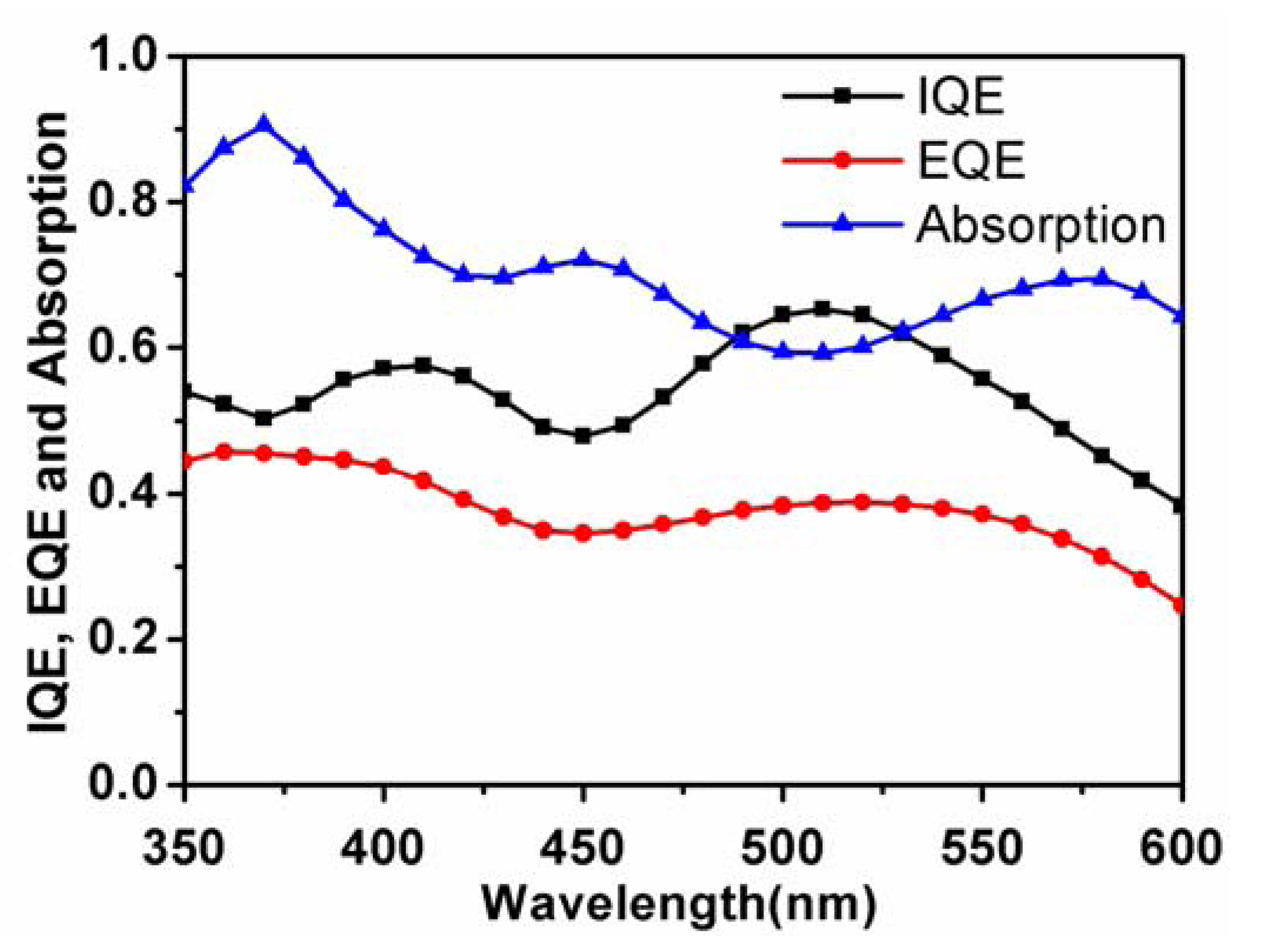
Finally, it is a question that whether the low photocurrent of D149 based solar cells comes from the limitation of charge separation and collection processes. In
Figure 5, we measured the absorption of the D149 based bilayer device, and calculated the internal quantum efficiency (IQE) by the use of the observed EQE spectrum. In a broad region from 350–600 nm, the IQE values of the solar cell were more than 40%. The light-harvesting capability of the solar cell contributes ~20% of the energy loss, while the other 30%–40% comes from the charge separation and charge transport within the solar cell device. Thus, further improvement of the carrier mobility of the indoline dye should be the key to improve the OPV performance. Moreover, about the charge separation mechanism in the present system, the clear EQE response from the absorption region of the D149 absorption peaks strongly suggests that the hot carriers was transferred to the acceptor molecules from the optically-transition-allowed electronic state of D149, as suggested in the investigation on carotenoid-based OSCs [
24].
Figure 5.
IQE, EQE and normalized absorption spectra for the bilayer device with the structure ITO/PEDOT: PSS (30 nm)/D149 (8 nm)/C70 (40 nm)/BCP (10 nm)/Al (100 nm).
Figure 5.
IQE, EQE and normalized absorption spectra for the bilayer device with the structure ITO/PEDOT: PSS (30 nm)/D149 (8 nm)/C70 (40 nm)/BCP (10 nm)/Al (100 nm).


