
Controlled Synthesis of Atomically Layered Hexagonal Boron Nitride via Chemical Vapor Deposition

Abstract
:1. Introduction
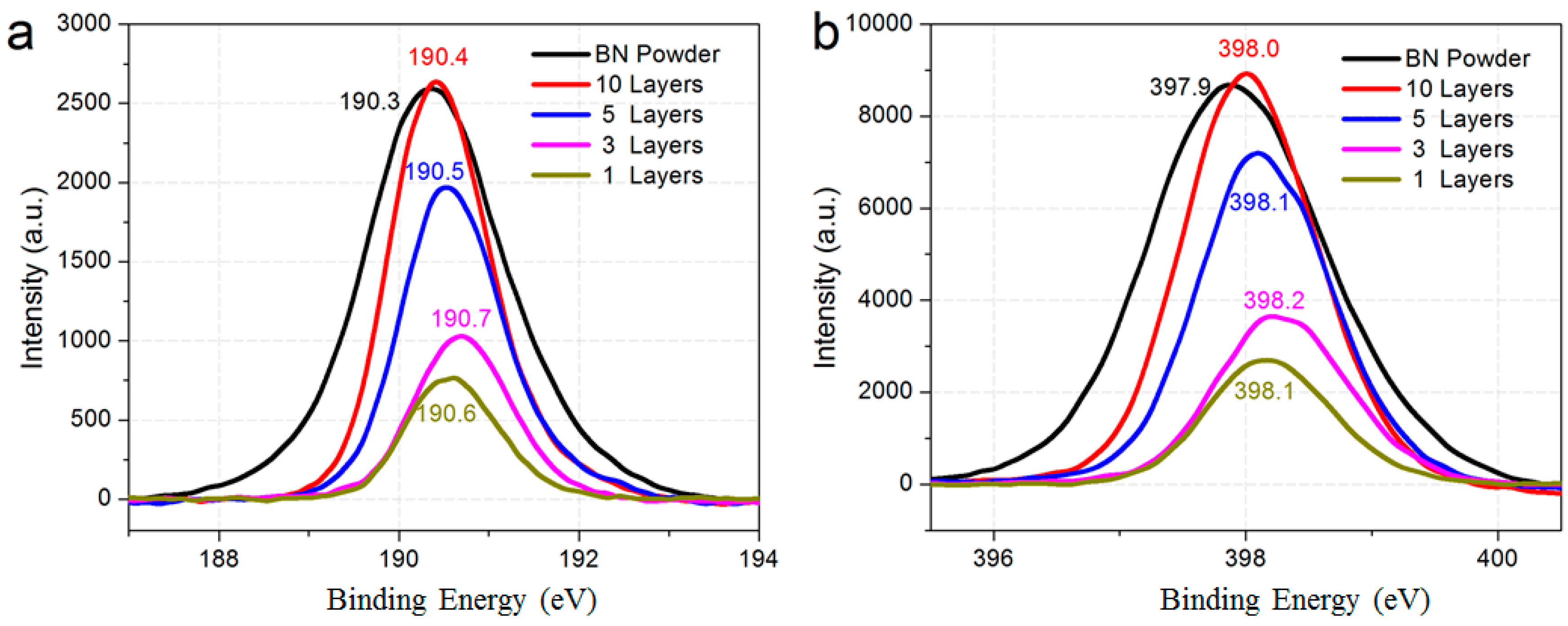
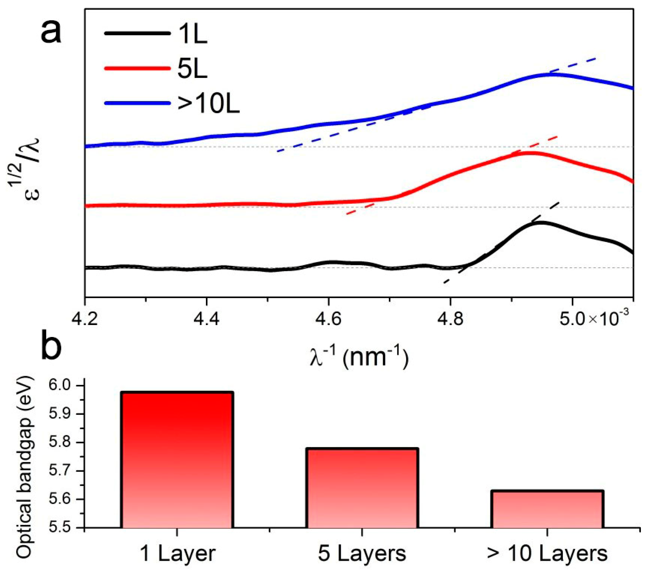
2. Results
3. Discussion
4. Materials and Methods
5. Conclusions
Supplementary Materials
Acknowledgments
Author Contributions
Conflicts of Interest
References
- Shi, Y.; Hamsen, C.; Jia, X.; Kim, K.; Reina, A.; Hofmann, M.; Hsu, A.; Zhang, K.; Li, H.; Juang, Z. Synthesis of Few-Layer Hexagonal Boron Nitride Thin Film by Chemical Vapor Deposition. Nano Lett. 2010, 10, 4134–4139. [Google Scholar] [CrossRef] [PubMed]
- Song, L.; Ci, L.; Lu, H.; Sorokin, P.; Jin, C.; Ni, J.; Kvashnin, A.; Kvashnin, D.; Lou, J.; Yakobson, B. Large Scale Growth and Characterization of Atomic Hexagonal Boron Nitride Layers. Nano Lett. 2010, 10, 3209–3215. [Google Scholar] [CrossRef] [PubMed]
- Ci, L.; Song, L.; Jin, C.; Jariwala, D.; Wu, D.; Li, Y.; Srivastava, A.; Wang, Z.; Storr, K.; Balicas, L. Atomic layers of hybridized boron nitride and graphene domains. Nat. Mater. 2010, 9, 430–435. [Google Scholar] [CrossRef] [PubMed]
- Xue, J.; Sanchez-Yamagishi, J.; Bulmash, D.; Jacquod, P.; Deshpande, A.; Watanabe, K.; Taniguchi, T.; Jarillo-Herrero, P.; LeRoy, B.J. Scanning tunnelling microscopy and spectroscopy of ultra-flat graphene on hexagonal boron nitride. Nat. Mater. 2011, 10, 282–285. [Google Scholar] [CrossRef] [PubMed]
- Dean, C.R.; Young, A.F.; Meric, I.; Lee, C.; Wang, L.; Sorgenfrei, S.; Watanabe, K.; Taniguchi, T.; Kim, P.; Shepard, K.L.; et al. Boron nitride substrates for high-quality graphene electronics. Nat. Nano 2010, 5, 722–726. [Google Scholar] [CrossRef] [PubMed]
- Corso, M.; Auwärter, W.; Muntwiler, M.; Tamai, A.; Greber, T.; Osterwalder, J. Boron Nitride Nanomesh. Science 2004, 303, 217–220. [Google Scholar] [CrossRef] [PubMed]
- Gorbachev, R.V.; Riaz, I.; Nair, R.R.; Jalil, R.; Britnell, L.; Belle, B.D.; Hill, E.W.; Novoselov, K.S.; Watanabe, K.; Taniguchi, T. Hunting for Monolayer Boron Nitride: Optical and Raman Signatures. Small 2011, 7, 465–468. [Google Scholar] [CrossRef] [PubMed]
- José Eduardo, P.; Renato Borges, P.; Adalberto, F. Bilayer graphene on h-BN substrate: Investigating the breakdown voltage and tuning the bandgap by electric field. J. Phys. Condens. Matter 2012, 24, 075301. [Google Scholar]
- Decker, R.G.; Wang, Y.; Brar, V.W.; Regan, W.; Tsai, H.-Z.; Wu, Q.; Gannett, W.; Zettl, A.; Crommie, M.F. Local Electronic Properties of Graphene on a BN Substrate via Scanning Tunneling Microscopy. Nano Lett. 2011, 11, 2291–2295. [Google Scholar] [CrossRef] [PubMed]
- Quhe, R.; Zheng, J.; Luo, G.; Liu, Q.; Qin, R.; Zhou, J.; Yu, D.; Nagase, S.; Mei, W.; Gao, Z. Tunable and sizable band gap of single-layer graphene sandwiched between hexagonal boron nitride. NPG Asia Mater. 2012, 4, e6. [Google Scholar] [CrossRef]
- Britnell, L.; Gorbachev, R.V.; Jalil, R.; Belle, B.D.; Schedin, F.; Mishchenko, A.; Georgiou, T.; Katsnelson, M.I.; Eaves, L.; Morozov, S.V. Field-Effect Tunneling Transistor Based on Vertical Graphene Heterostructures. Science 2012, 335, 947–950. [Google Scholar] [CrossRef] [PubMed] [Green Version]
- Han, W.; Taychatanapat, T.; Hsu, A.; Watanabe, K.; Taniguchi, T.; Jarillo-Herrero, P.; Palacios, T. BN/Graphene/BN Transistors for RF Applications. Electron. Device Lett. IEEE 2011, 32, 1209–1211. [Google Scholar] [Green Version]
- Bokdam, M.; Khomyakov, P.A.; Brocks, G.; Zhong, Z.; Kelly, P.J. Electrostatic Doping of Graphene through Ultrathin Hexagonal Boron Nitride Films. Nano Lett. 2011, 11, 4631–4635. [Google Scholar] [CrossRef] [PubMed]
- Fan, Y.; Zhao, M.; Wang, Z.; Zhang, X.; Zhang, H. Tunable electronic structures of graphene/boron nitride heterobilayers. Appl. Phys. Lett. 2011, 98, 083103. [Google Scholar] [CrossRef]
- Kharche, N.; Nayak, S.K. Quasiparticle Band Gap Engineering of Graphene and Graphone on Hexagonal Boron Nitride Substrate. Nano Lett. 2011, 11, 5274–5278. [Google Scholar] [CrossRef] [PubMed]
- Ramasubramaniam, A.; Naveh, D.; Towe, E. Tunable Band Gaps in Bilayer Graphene-BN Heterostructures. Nano Lett. 2011, 11, 1070–1075. [Google Scholar] [CrossRef] [PubMed]
- Pacile, D.; Meyer, J.C.; Girit, C.O.; Zettl, A. The two-dimensional phase of boron nitride: Few-atomic-layer sheets and suspended membranes. Appl. Phys. Lett. 2008, 92, 133107. [Google Scholar] [CrossRef]
- Paine, R.T.; Narula, C.K. Synthetic routes to boron nitride. Chem. Rev. 1990, 90, 73–91. [Google Scholar] [CrossRef]
- Taniguchi, T.; Watanabe, K. Synthesis of high-purity boron nitride single crystals under high pressure by using Ba–BN solvent. J. Cryst. Growth 2007, 303, 525–529. [Google Scholar] [CrossRef]
- Watanabe, K.; Taniguchi, T.; Kanda, H. Direct-bandgap properties and evidence for ultraviolet lasing of hexagonal boron nitride single crystal. Nat. Mater. 2004, 3, 404–409. [Google Scholar] [CrossRef] [PubMed]
- Liu, Z.; Song, L.; Zhao, S.; Huang, J.; Ma, L.; Zhang, J.; Lou, J.; Ajayan, P.M. Direct Growth of Graphene/Hexagonal Boron Nitride Stacked Layers. Nano Lett. 2011, 11, 2032–2037. [Google Scholar] [CrossRef] [PubMed]
- Kim, K.K.; Hsu, A.; Jia, X.; Kim, S.; Shi, Y.; Hofmann, M.; Nezich, D.; Joaquin, F.; Nieva, R.; Dresselhaus, M. Synthesis of Monolayer Hexagonal Boron Nitride on Cu Foil Using Chemical Vapor Deposition. Nano Lett. 2011, 12, 161–166. [Google Scholar] [CrossRef] [PubMed]
- Wang, B.; Bocquet, M.-L. Monolayer Graphene and h-BN on Metal Substrates as Versatile Templates for Metallic Nanoclusters. J. Phys. Chem. Lett. 2011, 2, 2341–2345. [Google Scholar] [CrossRef]
- Lee, Y.; Liu, K.K.; Lu, A.; Wu, C.; Lin, C.; Zhang, W.; Su, W.; Hsu, C.; Lin, T.; Wei, K. Growth selectivity of hexagonal-boron nitride layers on Ni with various crystal orientations. RSC Adv. 2012, 2, 111–115. [Google Scholar] [CrossRef]
- Geick, R.; Perry, C.H.; Rupprecht, G. Normal Modes in Hexagonal Boron Nitride. Phys. Rev. 1966, 146, 543. [Google Scholar] [CrossRef]
- Babich, I.L. Raman spectrum of hexagonal boron nitride. Theor. Exp. Chem. 1974, 8, 594–595. [Google Scholar] [CrossRef]
- Kubota, Y.; Watanabe, K.; Tsuda, O.; Taniguchi, T. Deep Ultraviolet Light-Emitting Hexagonal Boron Nitride Synthesized at Atmospheric Pressure. Science 2007, 317, 932–934. [Google Scholar] [CrossRef] [PubMed]
- Watanabe, K.; Taniguchi, T. Hexagonal Boron Nitride as a New Ultraviolet Luminescent Material and Its Application. Int. J. Appl. Ceram. Technol. 2011, 8, 977–989. [Google Scholar] [CrossRef]
- Li, L.H.; Chen, Y.; Lin, M.-Y.; Glushenkov, A.M.; Cheng, B.-M.; Yu, J. Single deep ultraviolet light emission from boron nitride nanotube film. Appl. Phys. Lett. 2010, 97, 141104. [Google Scholar] [CrossRef]
- Blase, X.; Rubio, A.; Louie, S.G.; Cohen, M.L. Quasiparticle band structure of bulk hexagonal boron nitride and related systems. Phys. Rev. B 1995, 51, 6868–6875. [Google Scholar] [CrossRef]
- Hoffman, D.M.; Doll, G.L.; Eklund, P.C. Optical properties of pyrolytic boron nitride in the energy range 0.05–10 eV. Phys. Rev. B 1984, 30, 6051–6056. [Google Scholar] [CrossRef]
- Lee, K.H.; Shin, H.-J.; Lee, J.; Lee, I.-Y.; Kim, G.-H.; Choi, J.-Y.; Kim, S.-W. Large-Scale Synthesis of High-Quality Hexagonal Boron Nitride Nanosheets for Large-Area Graphene Electronics. Nano Lett. 2012, 12, 714–718. [Google Scholar] [CrossRef] [PubMed]
- Sample Availability: Samples of the h-BN films are available from the authors.


| Thickness of h-BN | 1–2 L | 2–3 L | 5–6 L | Few Layers | Bulk |
|---|---|---|---|---|---|
| Growth temperature | 1000 °C | 1000 °C | 1000 °C | 1000 °C | >1100 °C |
| Growth time | 1 h | 1.5 h | 1 h | 1 h | 0.5 h |
| Precursor temperature | 40 °C | 40 °C | 50 °C | 70 °C | 70 °C |
© 2016 by the authors. Licensee MDPI, Basel, Switzerland. This article is an open access article distributed under the terms and conditions of the Creative Commons Attribution (CC-BY) license ( http://creativecommons.org/licenses/by/4.0/).
Share and Cite
Liu, J.; Kutty, R.G.; Liu, Z. Controlled Synthesis of Atomically Layered Hexagonal Boron Nitride via Chemical Vapor Deposition. Molecules 2016, 21, 1636. https://doi.org/10.3390/molecules21121636
Liu J, Kutty RG, Liu Z. Controlled Synthesis of Atomically Layered Hexagonal Boron Nitride via Chemical Vapor Deposition. Molecules. 2016; 21(12):1636. https://doi.org/10.3390/molecules21121636
Chicago/Turabian StyleLiu, Juanjuan, R. Govindan Kutty, and Zheng Liu. 2016. "Controlled Synthesis of Atomically Layered Hexagonal Boron Nitride via Chemical Vapor Deposition" Molecules 21, no. 12: 1636. https://doi.org/10.3390/molecules21121636
APA StyleLiu, J., Kutty, R. G., & Liu, Z. (2016). Controlled Synthesis of Atomically Layered Hexagonal Boron Nitride via Chemical Vapor Deposition. Molecules, 21(12), 1636. https://doi.org/10.3390/molecules21121636