Article

Synthesis and Study of Fe-Doped Bi2S3 Semimagnetic Nanocrystals Embedded in a Glass Matrix

1
Departamento de Física, Instituto de Ciências Exatas, Naturais e Educação (ICENE), Universidade Federal do Triângulo Mineiro, Uberaba 38025–180, Minas Gerais, Brazil
2
Departamento de Engenharia Mecânica, Instituto de Ciências Tecnológicas e Exatas (ICTE), Universidade Federal do Triângulo Mineiro, Uberaba 38064–200, Minas Gerais, Brazil
3
Instituto do Mar, Universidade Federal de São Paulo, Santos 11070–100, São Paulo, Brazil
4
Laboratório de Novos Materiais Isolantes e Semicondutores (LNMIS), Instituto de Física, Universidade Federal de Uberlândia, Uberlândia 38400–902, Minas Gerais, Brazil
*
Author to whom correspondence should be addressed.
Molecules 2017, 22(7), 1142; https://doi.org/10.3390/molecules22071142
Submission received: 28 May 2017 / Revised: 3 July 2017 / Accepted: 5 July 2017 / Published: 11 July 2017
(This article belongs to the Special Issue Nanocrystals: Synthesis, Characterization and Applications)

Abstract

:
Iron-doped bismuth sulphide (Bi2−xFexS3) nanocrystals have been successfully synthesized in a glass matrix using the fusion method. Transmission electron microscopy images and energy dispersive spectroscopy data clearly show that nanocrystals are formed with an average diameter of 7–9 nm, depending on the thermic treatment time, and contain Fe in their chemical composition. Magnetic force microscopy measurements show magnetic phase contrast patterns, providing further evidence of Fe incorporation in the nanocrystal structure. The electron paramagnetic resonance spectra displayed Fe3+ typical characteristics, with spin of 5/2 in the 3d5 electronic state, thereby confirming the expected trivalent state of Fe ions in the Bi2S3 host structure. Results from the spin polarized density functional theory simulations, for the bulk Fe-doped Bi2S3 counterpart, corroborate the experimental fact that the volume of the unit cell decreases with Fe substitutionally doping at Bi1 and Bi2 sites. The Bader charge analysis indicated a pseudo valency charge of 1.322|e| on FeBi1 and 1.306|e| on FeBi2 ions, and a spin contribution for the magnetic moment of 5.0 µB per unit cell containing one Fe atom. Electronic band structures showed that the (indirect) band gap changes from 1.17 eV for Bi2S3 bulk to 0.71 eV (0.74 eV) for Bi2S3:FeBi1 (Bi2S3:FeBi2). These results are compatible with the 3d5 high-spin state of Fe3+, and are in agreement with the experimental results, within the density functional theory accuracy.

Graphical Abstract

1. Introduction

Semiconductor nanocrystals doped with transition metals constitute a class of new nanomaterials that have been intensively investigated recently, mainly due to their interesting and tunable physical properties, which are significantly different from that of the nonmagnetic host semiconductor nanocrystal [1,2,3,4]. These materials, in which the magnetic dopant concentration is typically a few percentage points, are known as diluted magnetic semiconductors (DMS). The main cause of the new physical properties owned by these DMS materials is attributed to the sp- exchange interaction between the host nonmagnetic semiconductor sp-band and the partially occupied transition metal d-state [5,6,7]. Synthesis of several kinds of transition metal doped semiconductor nanocrystals are reported in the literature, such as Mn-doped Bi2S3 [8] and PbSe [9], Cu-doped SrF2 [10], Co-doped PbSe [11], Cr-doped In2O3 [12], and Fe-doped ZnO [13], PbTiO3 [14], and TiO2 [15]. These DMS nanocrystals can be applied in light-emitting diodes (LEDs) [16], solar cells [17], optical ratio-metric temperature sensors [18], and spintronic devices [19].
One material that has potential technological applications to be explored, and which present interesting electronic properties, is the bismuth sulphide (Bi2S3) semiconductor [20,21]. For Bi2S3 bulk, it has been reported a direct band gap of 1.3–1.7 eV [22,23,24], from both experimental and theoretical methods with the framework of the GW DFT (Green function and screened coulomb interaction), whereas standard DFT reports indirect band gap of 1.19 eV [25]. Bi2S3 crystallizes in the orthorhombic structure (Pnma space group), with a unit cell consisting of four Bi2S3 units, leading to a 20 atoms unit cell [26]. Each Bi2S3 unit has two nonequivalent Bi sites, denoted as Bi1 and Bi2, which differs in their coordination, as well as three nonequivalent S sites, denoted as S1–S3.
The electronic properties of semiconductor nanocrystals can be tunable by means of quantum confinement effects, as well as by doping with magnetic ions [27,28]. Therefore, doping Bi2S3 nanocrystals with Fe ions could lead to physical properties tunable by size and dopant concentration control. As Fe ions enter into the Bi2S3 structure, most probably as Fe3+ substituting Bi3+ ions, with 3d5 valence configuration and spin of 5/2 [29], it became possible to add magnetic properties to the nonmagnetic Bi2S3 nanocrystals. The exchange interaction between the sp-band from the Bi2S3 semiconductor, and the d-state from the Fe3+ ion become important for their electronic and, consequently, optical properties.
In this work, we report the synthesis and study of iron-doped bismuth sulphide (Bi2−xFexS3) nanocrystals embedded in a host glass matrix (referred to as SNAB) by the fusion method, with Fe-concentration of x = 0.00, x = 0.05, and x = 0.10. The SNAB glass matrix was chosen because it presents good chemical stability, optical transparency in the visible and near-infrared spectra regions, and is nontoxic, which makes it an excellent template for the growth of different kinds of nanocrystals [8,30,31,32]. The structural and magnetic properties of Bi2−xFexS3 nanocrystals were investigated experimentally by the techniques of transmission electron microscopy (TEM), energy dispersive spectroscopy (EDS), atomic and magnetic force microscopy (AFM/MFM), and electron paramagnetic resonance (EPR). In order to gain insight into the Fe-doping effect on the structural parameters of Bi2S3 nanocrystals, a theoretical study was performed on Fe-doped bulk Bi2S3, based on density functional theory (DFT), using pseudopotentials and numerical atomic basis set.

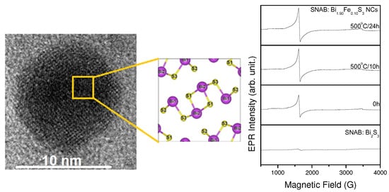
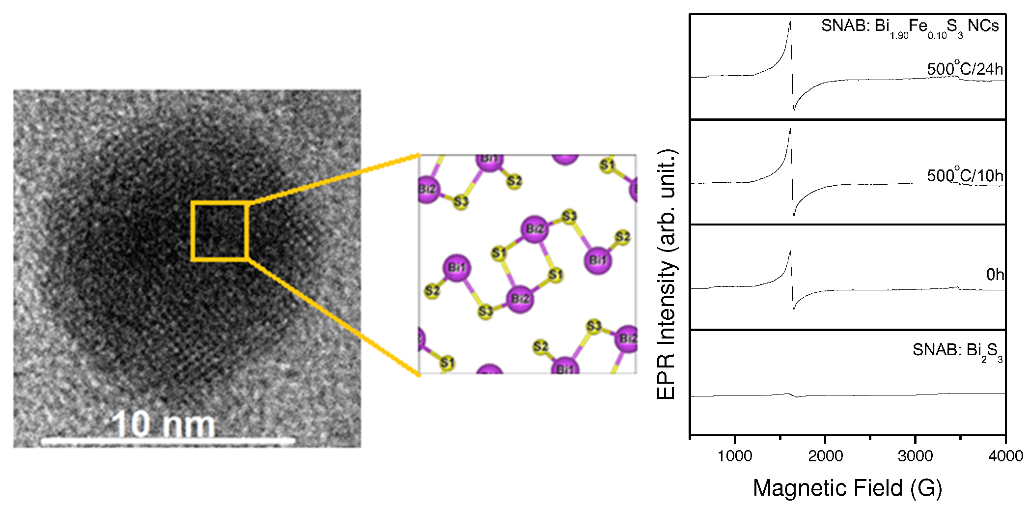
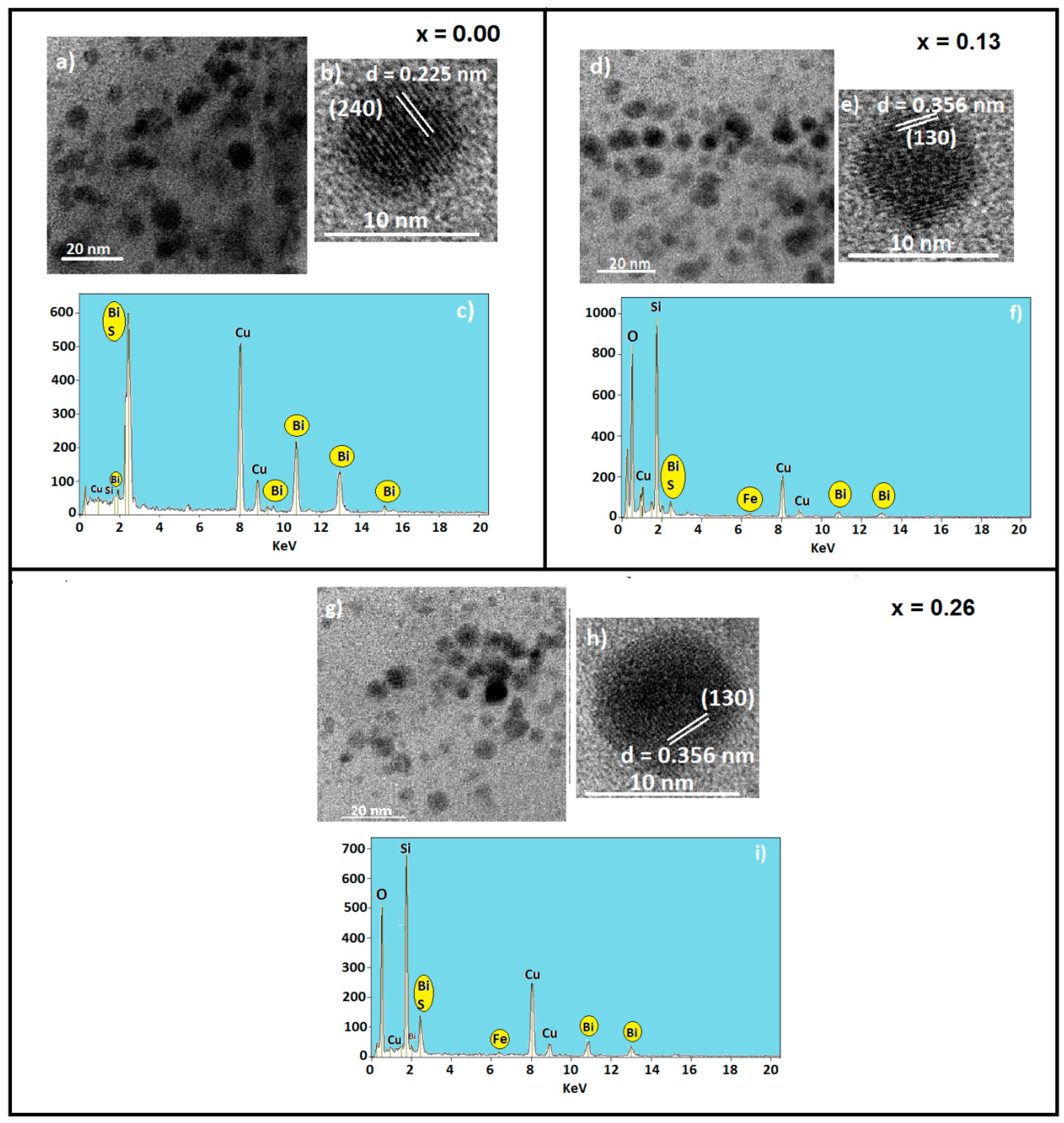
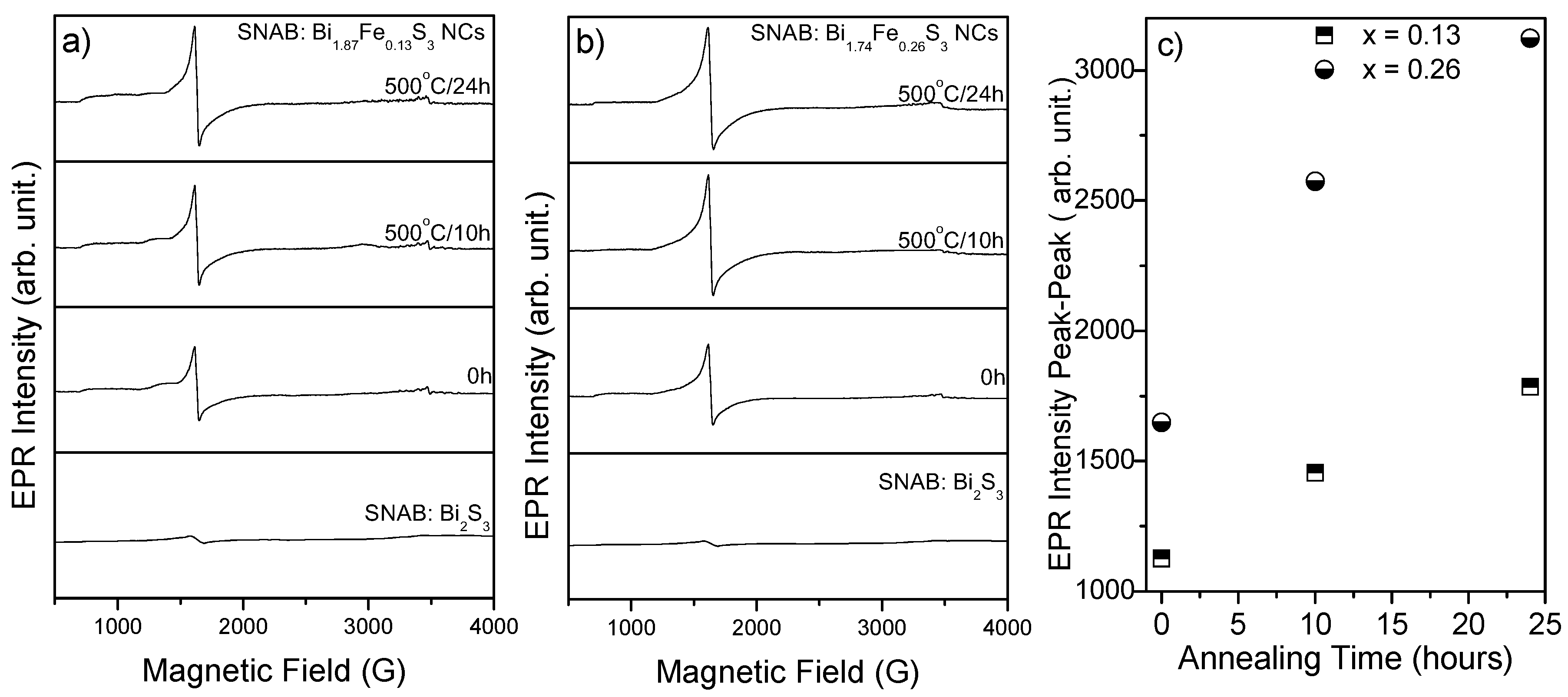
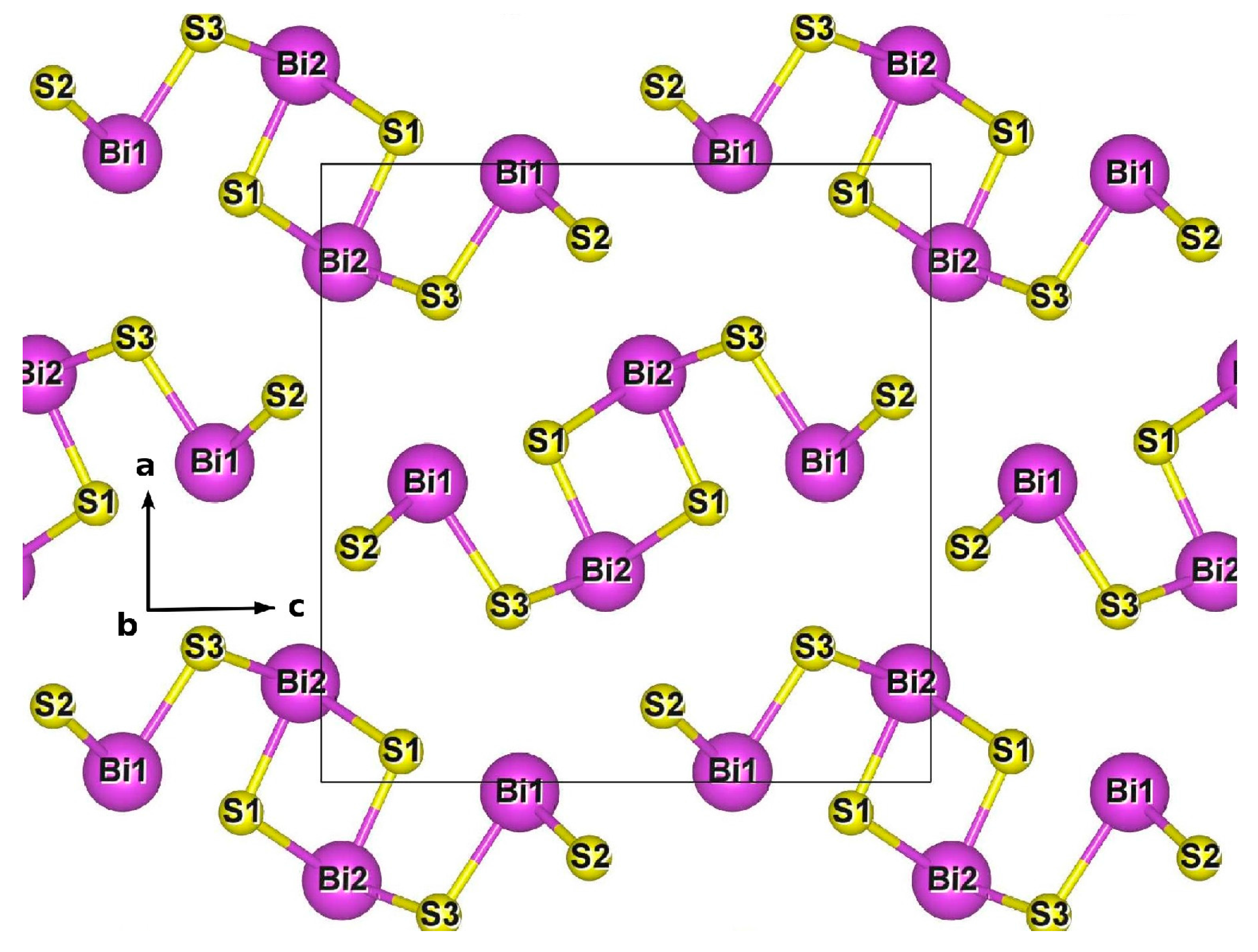
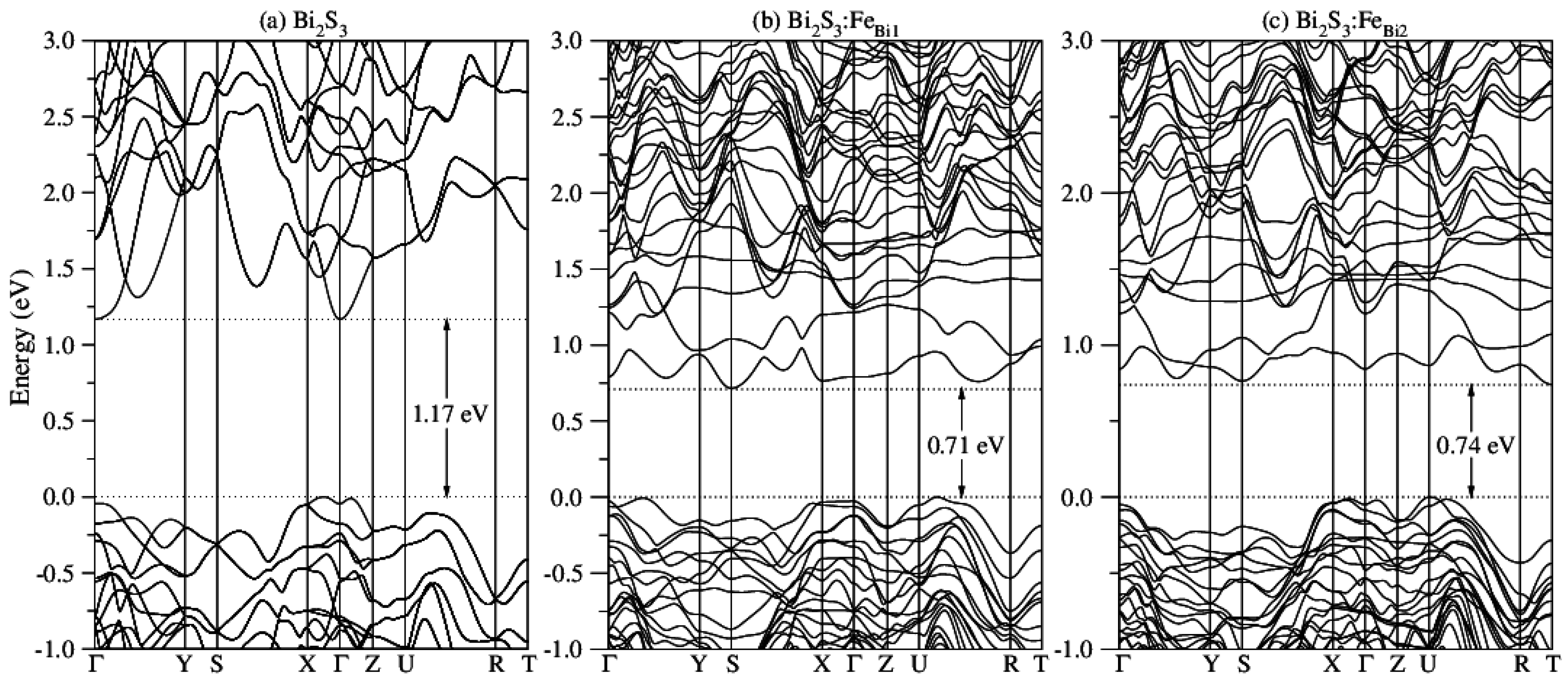
2. Results and Discussion

TEM images of Bi2−xFexS3 nanocrystals growth in the SNAB glass matrix, and those thermally treated at 500 °C for 10 h, are displayed in Figure 1 for (a) x = 0.00, (d) x = 0.13, and (g) x = 0.26, as well as a correspondent nanocrystal magnified image for the samples thermally treated at 500 °C for 24 h (Figure 1b,e,h) and the EDS data (Figure 1c,f,i). An average diameter of 7 nm has been obtained. From the magnified TEM images (to samples treated for 24 h), the mean diameter of the single nanocrystal is 9 nm, the interplanar distance of d240 = 0.225 nm (x = 0.00) and d130 = 0.356 nm (x = 0.13 and 0.26) was estimated and attributed to the bulk Bi2S3 (240) and (130) crystalline planes, respectively. These estimations were done with the software ImageJ [33]. EDS measurements of the samples treated for 10 h, confirm the chemical composition of the Fe-doped Bi2S3 nanocrystals. The presence of Fe can be seen at about 6.4 keV in the EDS spectrum.
Figure 2 shows the AFM/MFM images (700 × 700 nm) used for magnetic investigations of Bi2−xFexS3 nanocrystals, with an average size of 9.0 nm (obtained by TEM images), being: (a) x = 0.00, (b) x = 0.13, and (c) x = 0.26. Topographic images are shown in the left panels, and corresponding magnetic phase images are shown in the right panels. The bright/dark contrast in the MFM magnetic phase images is attributed to the magnetic response of Bi2−xFexS3 nanocrystals when induced by a magnetized tip. The bright/dark contrast is due to the repulsion/attraction of the magnetized tip to the nanocrystals, represented in the vertical bar, as with the north (N) (south (S)) poles [34]. The same contrast does not appear for the sample containing only non-doped Bi2S3 nanocrystals (x = 0.00). These AFM/MFM images support TEM/EDS data and EPR measurements, providing evidence of the incorporation of Fe3+ magnetic ions into the crystalline structure of Bi2−xFexS3 nanocrystals.
EPR measurements were carried out at 300 K and at X-band frequencies on Bi2−xFexS3 nanocrystals grown in the SNAB matrix. Fe3+ ions (3d5, S = 5/2) have typical absorptions at g-factor equal to 4.30 and 2.00. In general, the spin Hamiltonian for Fe3+ ions is represented by [29]
H = g μ B H . S + D { S z 2 + ( S ( S + 1 ) 3 ) } + E ( S x 2 S y 2 )
Here, g is gyromagnetic factor, μ B is the Bohr magneton, H is the applied magnetic field, S the effective spin of the Fe3+ ion, Si(i = x, y, z) are the spin angular momentum operators in the coordinate system. The terms D and E are the second order terms of the crystalline field, with axial and rhombic symmetry, respectively, and represent the interaction with the zero magnetic field. The Hamiltonian spin of the Fe3+ ion is strongly dependent on the D value, providing a value of the g-factor close to 2.0023 when D smaller than μ B H , independent of E. However, when the term D is greater than g μ B H , the g-factor has values around g = 4.3 (E ≠ 0) and g = 6.0 (E = 0). In literature, the absorptions at g = 4.3 and g = 6.0 are attributed to the location of the Fe3+ ions in tetrahedral or octahedral sites [35,36]. In Figure 3, the EPR spectra are presented for the untreated samples and for samples treated at 500°C for 10 and 24 h. These spectra are for sample with (a) x = 0.13 and (b) x = 0.26. The annealing treatment increases the size of the Bi2−xFexS3 nanocrystals and, consequently, increases the intensity which is attributed to a greater incorporation of the Fe3+ ions, as substitution for the ions of Bi3+, in the crystalline structure of the Bi2S3 semiconductor. In the particular case of x = 0.00, the EPR signal of Fe3+ ions are not observed. This increase in the peak-to-peak intensity of the Fe3+ ion EPR signal is attributed to the influence of the crystalline field of the Bi2S3 nanocrystals and is analyzed in Figure 3c for the concentrations of x = 0.05 and 0.10. The EPR spectra amplitude was normalized by the mass of the samples. The EPR data is in agreement with the results obtained by TEM/EDS and AFM/MFM.
The orthorhombic unit cell used in the DFT simulation of bulk Bi2S3 is illustrated in Figure 4. It consists of 8 Bi and 12 S atoms, adding up to 20 atoms per unit cell. The optimized lattice parameters and unit cell volume of bulk Bi2S3 crystal structure at zero pressure are collected in Table 1, and are compared with the correspondent experimental values from Lundegaard et al. [26]. The calculated lattice parameters and unit cell volume for bulk Bi2S3 crystal structure are in excellent agreement with the experimental ones, within the DFT-GGA accuracy.
Data for crystal structures of Fe-doped Bi2S3 are also collected in Table 1 for Fe occupying Bi1 or Bi2 sites. The results show that when bulk Bi2S3 is doped with Fe, the unit cell decreases in volume by a factor of 3.6% for FeBi1 and of 1.9% for FeBi2. Total energy calculations show that FeBi1 structure is energetically favorable relative to FeBi2 by only 289 meV, which means that both Bi sites are almost just as likely to be occupied by Fe atoms. Results from Bader charge analysis [42,43] are displayed in Table 2, showing a pseudo valency charge of 1.322|e| on FeBi1 and 1.306|e| on FeBi2 ions, which compares well with the pseudo valency charge of 1.454|e| and 1.600|e| on Bi1 and Bi2 sites at Bi2S3 undoped structure, with small charge transfer among atoms. For Fe-doped Bi2S3 bulk, Bader charges and pseudo valency charges on different Bi and S sites change very little and are not shown in Table 2. For both Fe-doped structures, a spin contribution for the magnetic moment of 5.0 μB per unit cell containing one Fe atom was obtained.
The energy band structure of Bi2S3 bulk and Fe-doped Bi2S3, along the high symmetry directions in the Brillouin zone, are shown in Figure 5. For Bi2S3, the band structure (Figure 5a) indicate an indirect band gap of 1.17 eV, with valence band maximum (VBM) within the X–Γ line and conduction band minimum (CBM) at the Γ point, which is in good agreement with other theoretical calculations [25]. Iron doping results in a reduction of the band gap to 0.71 eV for Fe atoms occupying Bi1 sites (Figure 5b) and to 0.74 eV for Fe atoms occupying Bi2 sites (Figure 5c), due to energy levels introduced by Fe orbitals.

3. Materials and Methods

Bi2−xFexS3 nanocrystal samples were synthesized by the fusion method in a borosilicate glass matrix, referred to as SNAB, with the following nominal composition: 45SiO2·30Na2CO3·5Al2O3·20B2O3 (mol %), and adding 2% of Bi2O3 and S (wt), and nominal x content of Fe (x = 0.00, 0.13, and 0.26) as a function of bismuth concentration. The powder mixture of the glass and the nanocrystal precursors were combined and melted in an alumina crucible, at 1200 °C for 30 min, and then rapidly cooled at room temperature. The resulting samples were then thermally treated in ambient air at 500 °C for 10 and 24 h to provide the energy and time needed for the diffusion of the Bi3+, S2−, and Fe3+ ions throughout the host matrix. This annealing process produces Fe-doped Bi2S3 nanocrystals with small size distribution. TEM micrographs and EDS were taken using a JEM-2100 (JEOL, 200 kV) to investigate the formation, size, shape, and growth of the Bi2−xFexS3 nanocrystals. Since TEM images of dielectric materials (glass template) are difficult to obtain, the samples were turned into a finer powder, and placed on a plate made of copper in order of take the TEM measurements. AFM/MFM images were recorded in a Shimadzu (SPM-9600) scanning probe microscope, with nominal resolution in the vertical direction for topographic mode of 0.01 nm and horizontally of 0.2 nm. Iron magnetic impurity electronic states, in the structure of the doped nanocrystals, were studied via EPR, using a ST ER4102 spectrometer (Bruker EMX spectrometer) with a rectangular cavity, microwave frequency of 9.75 GHz (X-band), microwave power of 20 mW, and 100 kHz field modulation. All measurements were taken at room temperature.
In order to obtain the structural effect, the Bader charge analysis, and the spin contribution to the magnetic moment of Fe-doped Bi2S3 nanostructure, first principle simulations based on density functional theory [37,38] were carried out. All the simulations were performed using norm-conserving pseudopotentials [39] and the PBE generalized gradient approximation [40] for the electronic exchange-correlation functional, as implemented in the Siesta [41] code. Relativistic pseudopotentials, chosen to enable spin polarized simulations (without taking into account the spin-orbit interaction), were generated with the following valence configurations: 6s2 6p3 6d0 5f0 for Bi, 3s2 3p4 3d0 4f0 for S, and 3d6 4s2 4p0 4f0 for Fe.
One conventional unit cell of Bi2S3, containing 20 atoms (four stoichiometric Bi2S3 formulas) was used as a supercell. The experimental data for bulk Bi2S3 [26] was taken as the starting geometry. Then, full relaxation of lattice parameters and atomic coordinates were performed. For Fe-doped Bi2S3 simulations, starting from the full relaxed Bi2S3 bulk structure, one Bi atom (at Bi1 or Bi2 site) was substituted by one Fe atom per unit cell and fully relaxed again, getting an Fe atomic doping concentration of 12.5%. Indeed, this is a higher concentration, but it is near to the experimental concentration of the sample synthesized with 13.0% of Fe (nominal) concentration.
The following parameters were used for all the calculations: a DZP basis set with an energy shift of 100 meV, a mesh cutoff of 250 Ry (~3400 eV), a maximum difference tolerance in the density matrix of 1 × 10⁻⁵, a tolerance in the total free energy of 1 × 10⁻⁴ eV, 0.01 eV/Å for the force relaxation criterion, 0.05 GPa as the maximum difference in the stress tensor components, and 36 k-points in the unit cell for k-sampling in the Brillouin zone. Only for Bader charge analysis, a mesh cutoff of 300 Ry was set.

4. Conclusions

Diluted magnetic semiconductor nanocrystals of Bi2−xFexS3 have been successfully synthesized in a glass matrix by the fusion method. TEM measurements confirm the formation of nanocrystals with average diameter of 7 nm and 9 nm for samples thermally treated at 500 °C for 10 and 24 h, respectively. EDS measurement suggested that the Fe ions were incorporated in the nanocrystal structure, which is confirmed from the observed magnetic phase contrast in the AFM/MFM measurements, which is attributed to the magnetic response of Fe3+ ions in the nanocrystal structure. EPR spectra confirm the Fe3+ valence state with a spin of 5/2, and the crystalline field influence on the Bi2S3 nanocrystals. DFT simulations showed that when bulk Bi2S3 is doped with Fe, the unit cell decreases in volume by a factor of 3.6% for FeBi1 and of 1.9% for FeBi2, and that the FeBi1 structure is energetically favorable to FeBi2 by 289 meV. Bader charge analysis indicated a pseudo valency charge of 1.322|e| on FeBi1 and 1.306|e| on FeBi2 ions, and a spin contribution for the magnetic moment of 5.0 μB per unit cell containing one Fe atom, for both FeBi1 and FeBi2 doped structures. Calculated electronic band structures showed that the indirect band gap changes from 1.17 eV for Bi2S3 bulk to 0.71 eV (0.74 eV) for Bi2S3:FeBi1 (Bi2S3:FeBi2).

Supplementary Materials

Supplementary File 1

Acknowledgments

The authors gratefully acknowledge financial support from the following Brazilian agencies: MCT/CNPq, Capes, Fapemig, and Rede Mineira de Química (RQ-MG) supported by Fapemig (project CEX-RED-00010-4). We are also thankful for use of the facilities for the TEM measurements at the Laboratório Multiusuário de Microscopia de Alta Resolução (LabMic), Universidade Federal de Goiás. HDM would like to acknowledge computing time provided by CENAPAD/Campinas-SP (proj 604).

Author Contributions

Ricardo S. Silva, E. V. Guimarães, and E. R. Gonçalves: Synthesis of Fe-doped Bi2S3 in glass matrix. N. F. Cano: provided measurements of electron paramagnetic resonance for support in data analysis. Noelio O. Dantas: provided measurements of atomic force microscopy for support in data analysis. H. D. Mikhail: carried out the computational calculations of density functional theory simulations.

Conflicts of Interest

The authors declare no conflict of interest.

References

  1. Erwin, S.C.; Zu, L.; Haftel, M.I.; Efros, A.L.; Kennedy, T.A.; Norris, D.J. Doping semiconductor nanocrystals. Nature 2005, 436, 91–94. [Google Scholar] [CrossRef] [PubMed]
  2. Karan, N.S.; Sarma, D.D.; Kadam, R.M.; Pradhan, N. Doping Transition Metal (Mn or Cu) Ions in Semiconductor Nanocrystals. J. Phys. Chem. Lett. 2010, 1, 2863–2866. [Google Scholar] [CrossRef]
  3. Silva, R.S.; Neto, E.S.F.; Dantas, N.O. Optical, Magnetic, and Structural Properties of Semiconductor and Semimagnetic Nanocrystals. In Nanocrystals—Synthesis, Characterization and Applications, 26th ed.; Neralla, S., Ed.; InTech: Rijeka, Croatia, 2012; Volume 3, pp. 61–80. [Google Scholar] [CrossRef]
  4. Jang, D.M.; Kwak, I.H.; Kwon, E.L.; Jung, C.S.; Im, H.S.; Park, K.; Park, J. Transition-Metal Doping of Oxide Nanocrystals for Enhanced Catalytic Oxygen Evolution. J. Phys. Chem. C 2015, 119, 1921–1927. [Google Scholar] [CrossRef]
  5. Furdyna, J.K. Diluted Magnetic Semiconductors. J. Appl. Phys. 1988, 64, R29–R64. [Google Scholar] [CrossRef]
  6. Archer, P.I.; Santangelo, S.A.; Gamelin, D.R. Direct Observation of sp-d exchange interactions in colloidal Mn2+- and Co2+-doped CdSe quantum dots. Nano Lett. 2007, 7, 1037–1043. [Google Scholar] [CrossRef] [PubMed]
  7. Rice, W.D.; Liu, W.; Baker, T.A.; Sinitsyn, N.A.; Klimov, V.I.; Crooker, S.A. Revealing giant internal magnetic fields due to spin fluctuations in magnetically doped colloidal nanocrystals. Nat. Nanotechnol. 2016, 11, 137–142. [Google Scholar] [CrossRef] [PubMed]
  8. Silva, R.S.; Silva, J.T.T.; Rocha, V.R.; Cano, N.F.; Silva, A.C.A.; Dantas, N.O. Synthesis Process Controlled of Semimagnetic Bi2–xMnxS3 Nanocrystals in a Host Glass Matrix. J. Phys. Chem. C 2014, 118, 18730–18735. [Google Scholar] [CrossRef]
  9. Lourenço, S.A.; Silva, R.S.; Dantas, N.O. Growth kinetic on the optical properties of the Pb1−xMnxSe nanocrystals embedded in a glass matrix: Thermal annealing and Mn2+ concentration. Phys. Chem. Chem. Phys. 2012, 14, 11040–11047. [Google Scholar] [CrossRef] [PubMed]
  10. Sarkar, S.; Chatti, M.; Adusumalli, V.N.K.B.; Mahalingam, V. Highly Selective and Sensitive Detection of Cu2+ Ions Using Ce(III)/Tb(III)-Doped SrF2 Nanocrystals as Fluorescent Probe. ACS Appl. Mater. Interfaces 2015, 7, 25702–25708. [Google Scholar] [CrossRef] [PubMed]
  11. Lourenço, S.A.; Silva, R.S.; Dantas, N.O. Tunable dual emission in visible and near-infrared spectra using Co -doped PbSe nanocrystals embedded in a chalcogenide glass matrix. Phys. Chem. Chem. Phys. 2016, 18, 23036–23043. [Google Scholar] [CrossRef] [PubMed]
  12. Farvid, S.S.; Ju, L.; Worden, M.; Radovanovic, P.V. Colloidal Chromium-Doped In2O3 Nanocrystals as Building Blocks for High-TC Ferromagnetic Transparent Conducting Oxide Structures. J. Phys. Chem. C 2008, 112, 17755–17759. [Google Scholar] [CrossRef]
  13. Zhou, D.; Kittilstved, K.R. Electron trapping on Fe3+ sites in photodoped ZnO colloidal nanocrystals. Chem. Commun. 2016, 52, 9101–9104. [Google Scholar] [CrossRef] [PubMed]
  14. Ren, Z.; Xu, G.; Wei, X.; Liu, Y.; Hou, X.; Du, P.; Weng, W.; Shen, G.; Han, G. Room-temperature ferromagnetism in Fe-doped PbTiO3 nanocrystals. Appl. Phys. Lett. 2007, 91, 063106. [Google Scholar] [CrossRef]
  15. Yu, S.; Yun, H.J.; Lee, D.M.; Yi, J. Preparation and characterization of Fe-doped TiO2 nanoparticles as a support for a high performance CO oxidation catalyst. J. Mater. Chem. 2012, 22, 12629–12635. [Google Scholar] [CrossRef]
  16. Jo, D.Y.; Kim, D.; Kim, J.H.; Chae, H.; Seo, H.J.; Do, Y.R.; Yang, H. Tunable White Fluorescent Copper Gallium Sulfide Quantum Dots Enabled by Mn Doping. ACS Appl. Mater. Interfaces 2016, 8, 12291–12297. [Google Scholar] [CrossRef] [PubMed]
  17. Halder, G.; Bhattacharyya, S. Plight of Mn Doping in Colloidal CdS Quantum Dots To Boost the Efficiency of Solar Cells. J. Phys. Chem. 2015, 119, 13404–13412. [Google Scholar] [CrossRef]
  18. Huang, G.; Wang, C.; Xu, X.; Cui, Y. An optical ratiometric temperature sensor based on dopant-dependent thermal equilibrium in dual-emitting Ag & Mn:ZnInS quantum dots. RSC Adv. 2016, 6, 58113–58117. [Google Scholar] [CrossRef]
  19. Žutić, I.; Petukhov, A. Spintronics: Shedding light on nanomagnets. Nat. Nanotechnol. 2009, 4, 623–625. [Google Scholar] [CrossRef] [PubMed]
  20. Ge, Z.H.; Zhang, B.P.; Li, J.F. Microstructure composite-like Bi2S3 polycrystals with enhanced thermoelectric properties. J. Mater. Chem. 2012, 22, 17589–17594. [Google Scholar] [CrossRef]
  21. Chmielowski, R.; Péré, D.; Bera, C.; Opahle, I.; Xie, W.; Jacob, S.; Capet, F.; Roussel, P.; Weidenkaff, A.; Madsen, G.K.H.; et al. Theoretical and experimental investigations of the thermoelectric properties of Bi2S3. J. Appl. Phys. 2015, 117, 125103. [Google Scholar] [CrossRef]
  22. Black, J.; Conwell, E.M.; Seigle, L.; Spencer, C.W. Electrical and Optical Properties of some M2V−BN3VI−B Semiconductors. J. Phys. Chem. Solids 1957, 2, 240–251. [Google Scholar] [CrossRef]
  23. Filip, M.R.; Patrick, C.E.; Giustino, F. GW quasiparticle band structures of stibnite, antimonselite, bismuthinite, and guanajuatite. Phys. Rev. B 2013, 87, 205125. [Google Scholar] [CrossRef]
  24. Stavila, V.; Whitmire, K.H.; Rusakova, I. Synthesis of Bi2S3 nanostructures from bismuth (III) thiourea and thiosemicarbazide complexes. Chem. Mater. 2009, 21, 5456–5465. [Google Scholar] [CrossRef]
  25. Sharma, Y.; Srivastava, P.; Dashora, A.; Vadkhiya, L.; Bhayani, M.K.; Jain, R.; Jani, A.R.; Ahuja, B.L. Electronic structure, optical properties and Compton profiles of Bi2S3 and Bi2Se3. Solid State Sci. 2012, 14, 241–249. [Google Scholar] [CrossRef]
  26. Lundegaard, L.F.; Makovicky, E.; Boffa-Ballaran, T.; Balic-Zunic, T. Crystal structure and cation lone electron pair activity of Bi2S3 between 0 and 10 GPa. Phys. Chem. Miner. 2005, 32, 578–584. [Google Scholar] [CrossRef]
  27. Ge, Z.H.; Zhang, B.P.; Liu, Y.; Li, J.F. Nanostructured Bi2−xCuxS3 bulk materials with enhanced thermoelectric performance. Phys. Chem. Chem. Phys. 2012, 14, 4475–4481. [Google Scholar] [CrossRef] [PubMed]
  28. Panmand, R.P.; Kumar, G.; Mahajan, S.M.; Kulkarni, M.V.; Kale, B.B.; Gosavic, S.W. Novel and stable Mn2+@Bi2S3 quantum dots–glass system with giant magneto optical Faraday rotations. J. Mater. Chem. C 2013, 1, 1203–1210. [Google Scholar] [CrossRef]
  29. Racen, H.; Schneider, H. EPR study of Fe3+ centers in cristobalite and tridymite. Am. Mineral. 1986, 71, 105–110. Available online: http://www.minsocam.org/ammin/AM71/AM71_105.pdf (accessed on 12 May 2017).
  30. Dantas, N.O.; Paula, P.M.N.; Silva, R.S.; López-Richard, V.; Marques, G.E. Radiative versus nonradiative optical processes in PbS nanocrystals. J. Appl. Phys. 2011, 109, 024308. [Google Scholar] [CrossRef]
  31. Silva, R.S.; Mikhail, H.D.; Pavani, R.; Cano, N.F.; Silva, A.C.A.; Dantas, N.O. Synthesis of diluted magnetic semiconductor Bi2−xMnxTe3 nanocrystals in a host glass matrix. J. Alloy. Compd. 2015, 648, 778–782. [Google Scholar] [CrossRef]
  32. Dantas, N.O.; Neto, E.S.F.; Silva, R.S.; Jesus, D.R.; Pelegrini, F. Evidence of Cd1-xMnxS Nanocrystal Growth in a Glass Matrix by the Fusion Method. Appl. Phys. Lett. 2008, 93, 193115-1–193115-3. [Google Scholar] [CrossRef]
  33. Rasband, W.S. ImageJ, U.S. National Institutes of Health: Bethesda, ML, USA, 1997–2016. Available online: http://imagej.nih.gov/ij/ (accessed on 14 May 2017).
  34. Dantas, N.O.; Silva, A.S.; Silva, A.C.A.; Neto, E.S.F. Atomic and Magnetic Force Microscopy of Semiconductor and Semimagnetic Nanocrystals Grown in Colloidal Solutions and Glass Matrices. In Optical Imaging: Technology, Methods and Applications, 1st ed.; Tanaka, A., Nakamura, B., Eds.; Nova Science Publishers: Hauppauge, NY, USA, 2012; Volume 1, pp. 109–132. [Google Scholar]
  35. Dantas, N.O.; Wayta, W.E.F.; Silva, A.C.A.; Cano, N.F.; Rodriguez, A.F.R.; Oliveira, A.C.; Garg, V.K.; Morais, P.C. Magnetic and optical investigation of SiO2·30Na2O·1Al2O3·(29 − x)B2O3·xFe2O3 glass matrix. Solid State Sci. 2012, 14, 1169–1174. [Google Scholar] [CrossRef]
  36. Iwamoto, N.; Makino, Y.; Kasahara, S. State of Fe3+ ion and Fe3+-F- Interaction in Calcium Fluorosilicate Glasses. J. Non-Cryst. Solids 1983, 55, 113–124. [Google Scholar] [CrossRef]
  37. Hohenberg, P.; Kohn, W. Inhomogeneous Electron Gas. Phys. Rev. 1964, 136, B864–B871. [Google Scholar] [CrossRef]
  38. Kohn, W.; Sham, L. Self-consistent equations including exchange and correlation effects. Phys. Rev. 1965, 140, A1133–A1138. [Google Scholar] [CrossRef]
  39. Troullier, N.; Martins, J.L. Efficient pseudopotentials for plane-wave calculations. Phys. Rev. B 1991, 43, 1993–2006. [Google Scholar] [CrossRef]
  40. Perdew, J.P.; Burke, K.; Ernzerhof, M. Generalized Gradient Approximation Made Simple. Phys. Rev. Lett. 1996, 77, 3865–3868. [Google Scholar] [CrossRef] [PubMed]
  41. Soler, J.M.; Artacho, E.; Gale, J.D.; García, A.; Junqueira, J.; Ordejón, P.; Sánchez-Portal, D. The SIESTA method for ab initio order-N materials simulation. J. Phys. Condens. Matter 2002, 14, 2745–2779. Available online: stacks.iop.org/JPhysCM/14/2745 (accessed on 15 May 2017).
  42. Bader, R.F. Atoms in Molecules: A Quantum Theory; Oxford University Press: New York, NY, USA, 1990. [Google Scholar]
  43. Yu, M.; Trinkle, D.R. Accurate and efficient algorithm for Bader charge integration. J. Chem. Phys. 2011, 134, 064111. [Google Scholar] [CrossRef] [PubMed]
Sample Availability: Samples of the compounds not are available from the authors.
Figure 1. TEM images of Bi2−xFexS3 nanocrystals grown in the SNAB glass matrix with mean size of 7.0 nm, for x values: (a) 0.00; (d) 0.13; and (g) 0.26 and from 9.0 nm to the values of x: (b) 0.00; (e) 0.13; and (h) 0.26. EDS measurements for samples treated at 500 °C for 10 h are given for x values: (c) 0.00; (f) 0.13; and (i) 0.26. The white circle in the TEM images indicates the region in which the EDS measurement was performed in the samples.
Molecules 22 01142 g001
Figure 2. AFM/MFM images of 700 × 700 nm of Bi2−xFexS3 nanocrystals grown in the SNAB glass matrix, heat treated at 500 °C for 24 h, at concentrations: (a) x = 0.00; (b) x = 0.13; and (c) x = 0.26. Sample topographic (left panel) and magnetic phase (right panel) identifies the orientation of the total magnetic moment of the DMS NCs.
Molecules 22 01142 g002
Figure 3. Bi2−xFexS3 nanocrystal EPR spectra grown in the SNAB glass matrix for: (a) x = 0.13 and (b) x = 0.26. SNAB: Bi2S3 is correspondent to the case where x = 0.00. In (c), the intensity variation of the EPR signal is shown for the samples without treatment and with treatment times of 10 and 24 h at 500 °C.
Molecules 22 01142 g003
Figure 4. Crystal structure of bulk Bi2S3, at zero pressure, showing the unit cell.
Molecules 22 01142 g004
Figure 5. First-principle band structures for (a) bulk Bi2S3, (b) Fe-doped Bi2S3 at Bi1 site, and (c) Fe-doped Bi2S3 at Bi2 site. Horizontal dashed lines indicate valence bands maximum (set to zero) and conduction bands minimum. The selected k points are Γ = (0,0,0), Y = (0,½,0), S = (½,½,0), X = (½,0,0), Z = (0,0, ½), U = (½,0,½), R = (½, ½, ½), and T = (0,½,½).
Molecules 22 01142 g005
Table 1. Calculated zero pressure lattice parameters and unit cell volumes for bulk Bi2S3, Fe-doped Bi2S3 at Bi1 and at Bi2 sites. Experimental data for bulk Bi2S3 at zero pressure was taken from Ref. [26]. For all the structures, α = β = γ = 90°.
Structural ParametersBi2S3 Exp.[26]Bi2S3Bi2S3:FeBi1Bi2S3:FeBi2
a (Å)11.28211.249 dev. −0.29%11.41911.229
b (Å)3.97284.0296 dev. 1.43%3.95403.9318
c (Å)11.13111.004 dev. −1.14%10.65211.077
Vuc3)498.4498.8 dev. 0.08%480.9489.1
Table 2. Bader charge calculated from pseudo valency electron density for Bi2S3 bulk, Fe-doped Bi2S3 bulk at Bi1 and at Bi2 sites. Pseudo valency charge is the difference between the free atom valency charge and the Bader charge. All charges in units of |e|, where e is the elementary charge.
StructureAtomBader ChargePseudo Valency Charge
Bi2S3Bi13.5461.454
Bi23.4001.600
S17.108−1.108
S26.986−0.986
S36.960−0.960
Bi2S3:FeBi1Fe16.6781.322
Bi2S3:FeBi2Fe26.6941.306

