
Energy-Level Interpretation of Carbazole Derivatives in Self-Assembling Monolayer
 , , , ,
Abstract
:
1. Introduction
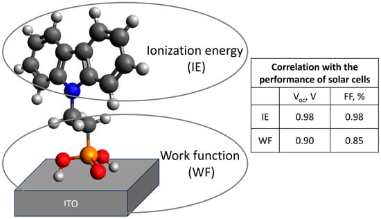
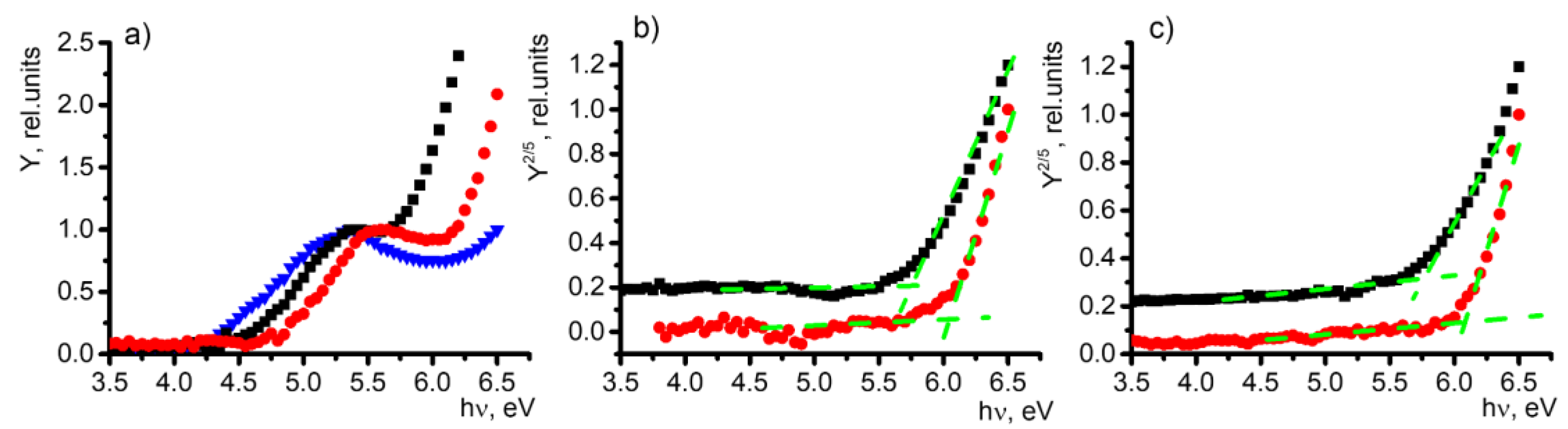
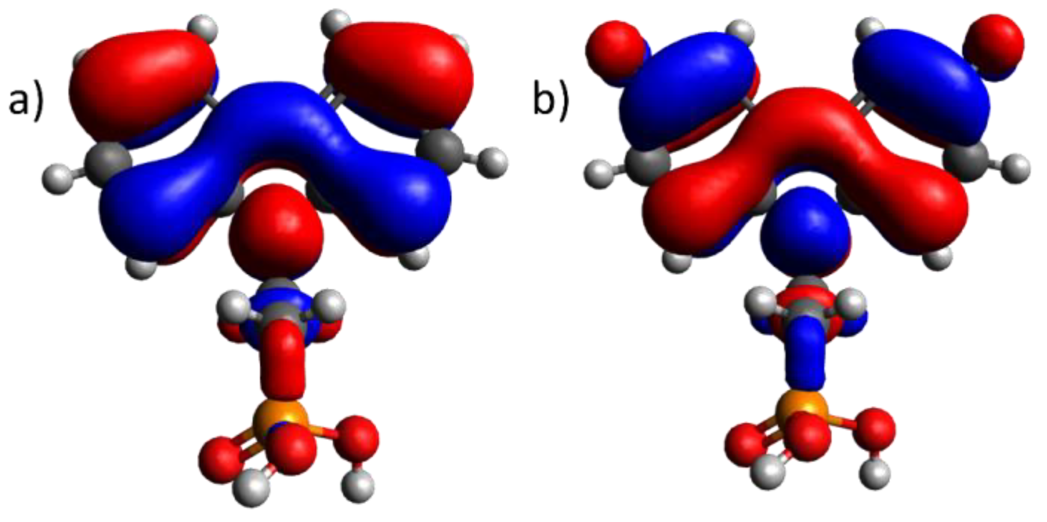
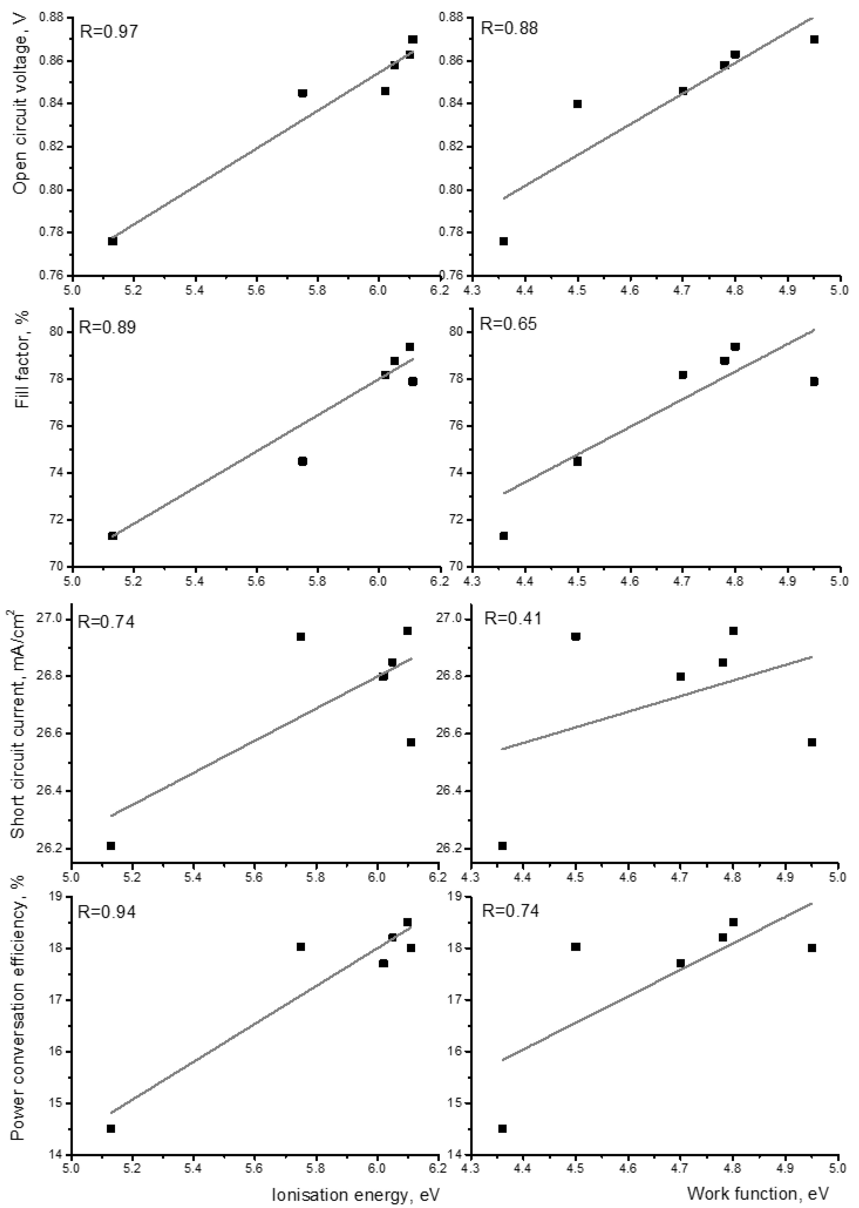
2. Discussion
3. Materials and Methods
3.1. Studied Materials
3.2. Sample Preparation
3.3. Film Characterization
3.4. Quantum Chemical Calculations
3.5. Solar Cell Performance Parameters
4. Conclusions
Supplementary Materials
Author Contributions
Funding
Institutional Review Board Statement
Informed Consent Statement
Data Availability Statement
Acknowledgments
Conflicts of Interest
References
- Zhou, Z.; Xie, X.; Sun, Z.; Wang, X.; An, Z.; Huang, W. Recent Advances in Metal-Free Phosphorescent Materials for Organic Light-Emitting Diodes. J. Mater. Chem. C Mater. 2023, 11, 3143–3161. [Google Scholar] [CrossRef]
- Krautmann, R.; Spalatu, N.; Josepson, R.; Nedzinskas, R.; Kondrotas, R.; Gržibovskis, R.; Vembris, A.; Krunks, M.; Oja Acik, I. Low Processing Temperatures Explored in Sb2S3 Solar Cells by Close-Spaced Sublimation and Analysis of Bulk and Interface Related Defects. Sol. Energy Mater. Sol. Cells 2023, 251, 112139. [Google Scholar] [CrossRef]
- Li, J.; Babuji, A.; Fijahi, L.; James, A.M.; Resel, R.; Salzillo, T.; Pfattner, R.; Ocal, C.; Barrena, E.; Mas-Torrent, M. Synergistic Effect of Solvent Vapor Annealing and Chemical Doping for Achieving High-Performance Organic Field-Effect Transistors with Ideal Electrical Characteristics. ACS Appl. Mater. Interfaces 2023, 15, 5521–5528. [Google Scholar] [CrossRef] [PubMed]
- Zhang, Y.; Xu, L.; Sun, J.; Wu, Y.; Kan, Z.; Zhang, H.; Yang, L.; Liu, B.; Dong, B.; Bai, X.; et al. 24.11% High Performance Perovskite Solar Cells by Dual Interfacial Carrier Mobility Enhancement and Charge-Carrier Transport Balance. Adv. Energy Mater. 2022, 12, 2201269. [Google Scholar] [CrossRef]
- Wu, J.; Cha, H.; Du, T.; Dong, Y.; Xu, W.; Lin, C.; Durrant, J.R. A Comparison of Charge Carrier Dynamics in Organic and Perovskite Solar Cells. Adv. Mater. 2022, 34, 2101833. [Google Scholar] [CrossRef] [PubMed]
- Chen, C.; Wu, C.; Ding, X.; Tian, Y.; Zheng, M.; Cheng, M.; Xu, H.; Jin, Z.; Ding, L. Constructing Binary Electron Transport Layer with Cascade Energy Level Alignment for Efficient CsPbI2Br Solar Cells. Nano Energy 2020, 71, 104604. [Google Scholar] [CrossRef]
- Karl, N. Charge Carrier Transport in Organic Semiconductors. Synth. Met. 2003, 133–134, 649–657. [Google Scholar] [CrossRef]
- Li, Y. Molecular Design of Photovoltaic Materials for Polymer Solar Cells: Toward Suitable Electronic Energy Levels and Broad Absorption. Acc. Chem. Res. 2012, 45, 723–733. [Google Scholar] [CrossRef] [PubMed]
- Zeng, J.; Bi, L.; Cheng, Y.; Xu, B.; Jen, A.K.-Y. Self-Assembled Monolayer Enabling Improved Buried Interfaces in Blade-Coated Perovskite Solar Cells for High Efficiency and Stability. Nano Res. Energy 2022, 1, e9120004. [Google Scholar] [CrossRef]
- Choi, K.; Choi, H.; Min, J.; Kim, T.; Kim, D.; Son, S.Y.; Kim, G.-W.; Choi, J.; Park, T. A Short Review on Interface Engineering of Perovskite Solar Cells: A Self-Assembled Monolayer and Its Roles. Sol. RRL 2020, 4, 1900251. [Google Scholar] [CrossRef]
- Casalini, S.; Bortolotti, C.A.; Leonardi, F.; Biscarini, F. Self-Assembled Monolayers in Organic Electronics. Chem. Soc. Rev. 2017, 46, 40–71. [Google Scholar] [CrossRef] [PubMed]
- Zuppiroli, L.; Si-Ahmed, L.; Kamaras, K.; Nüesch, F.; Bussac, M.N.; Ades, D.; Siove, A.; Moons, E.; Grätzel, M. Self-Assembled Monolayers as Interfaces for Organic Opto-Electronic Devices. Eur. Phys. J. B 1999, 11, 505–512. [Google Scholar] [CrossRef]
- Demirkan, K.; Mathew, A.; Weiland, C.; Yao, Y.; Rawlett, A.M.; Tour, J.M.; Opila, R.L. Energy Level Alignment at Organic Semiconductor/Metal Interfaces: Effect of Polar Self-Assembled Monolayers at the Interface. J. Chem. Phys. 2008, 128, 074705. [Google Scholar] [CrossRef] [PubMed]
- Ganzorig, C.; Kwak, K.-J.; Yagi, K.; Fujihira, M. Fine Tuning Work Function of Indium Tin Oxide by Surface Molecular Design: Enhanced Hole Injection in Organic Electroluminescent Devices. Appl. Phys. Lett. 2001, 79, 272–274. [Google Scholar] [CrossRef]
- Beaumont, N.; Hancox, I.; Sullivan, P.; Hatton, R.A.; Jones, T.S. Increased Efficiency in Small Molecule Organic Photovoltaic Cells through Electrode Modification with Self-Assembled Monolayers. Energy Environ. Sci. 2011, 4, 1708. [Google Scholar] [CrossRef]
- Hofmann, O.T.; Egger, D.A.; Zojer, E. Work-Function Modification beyond Pinning: When Do Molecular Dipoles Count? Nano Lett. 2010, 10, 4369–4374. [Google Scholar] [CrossRef] [PubMed]
- Hau, S.K.; Cheng, Y.-J.; Yip, H.-L.; Zhang, Y.; Ma, H.; Jen, A.K.-Y. Effect of Chemical Modification of Fullerene-Based Self-Assembled Monolayers on the Performance of Inverted Polymer Solar Cells. ACS Appl. Mater. Interfaces 2010, 2, 1892–1902. [Google Scholar] [CrossRef]
- Jiang, W.; Li, F.; Li, M.; Qi, F.; Lin, F.R.; Jen, A.K.-Y. Π-Expanded Carbazoles as Hole-Selective Self-Assembled Monolayers for High-Performance Perovskite Solar Cells. Angew. Chem. Int. Ed. 2022, 61, e202213560. [Google Scholar] [CrossRef] [PubMed]
- Yalcin, E.; Can, M.; Rodriguez-Seco, C.; Aktas, E.; Pudi, R.; Cambarau, W.; Demic, S.; Palomares, E. Semiconductor Self-Assembled Monolayers as Selective Contacts for Efficient PiN Perovskite Solar Cells. Energy Environ. Sci. 2019, 12, 230–237. [Google Scholar] [CrossRef]
- Whitten, J.E. Ultraviolet Photoelectron Spectroscopy: Practical Aspects and Best Practices. Appl. Surf. Sci. Adv. 2023, 13, 100384. [Google Scholar] [CrossRef]
- Grzibovskis, R.; Vembris, A.; Pudzs, K. Relation between Molecule Ionization Energy, Film Thickness and Morphology of Two Indandione Derivatives Thin Films. J. Phys. Chem. Solids 2016, 95, 12–18. [Google Scholar] [CrossRef]
- Seah, M.P.; Dench, W.A. Quantitative electron spectroscopy of surfaces: A standard data base for electron inelastic mean free paths in solids. Surf. Interface Anal. 1979, 1, 2–11. [Google Scholar] [CrossRef]
- Ozawa, Y.; Nakayama, Y.; Machida, S.; Kinjo, H.; Ishii, H. Maximum Probing Depth of Low-Energy Photoelectrons in an Amorphous Organic Semiconductor Film. J. Electron. Spectros Relat. Phenom. 2014, 197, 17–21. [Google Scholar] [CrossRef]
- Al-Ashouri, A.; Magomedov, A.; Roß, M.; Jošt, M.; Talaikis, M.; Chistiakova, G.; Bertram, T.; Márquez, J.A.; Köhnen, E.; Kasparavičius, E.; et al. Conformal Monolayer Contacts with Lossless Interfaces for Perovskite Single Junction and Monolithic Tandem Solar Cells. Energy Environ. Sci. 2019, 12, 3356–3369. [Google Scholar] [CrossRef]
- Lin, Y.; Zhang, Y.; Zhang, J.; Marcinskas, M.; Malinauskas, T.; Magomedov, A.; Nugraha, M.I.; Kaltsas, D.; Naphade, D.R.; Harrison, G.T.; et al. 18.9% Efficient Organic Solar Cells Based on n-Doped Bulk-Heterojunction and Halogen-Substituted Self-Assembled Monolayers as Hole Extracting Interlayers. Adv. Energy Mater. 2022, 12, 2202503. [Google Scholar] [CrossRef]
- Lin, Y.; Magomedov, A.; Firdaus, Y.; Kaltsas, D.; El-Labban, A.; Faber, H.; Naphade, D.R.; Yengel, E.; Zheng, X.; Yarali, E.; et al. 18.4 % Organic Solar Cells Using a High Ionization Energy Self-Assembled Monolayer as Hole-Extraction Interlayer. ChemSusChem 2021, 14, 3569–3578. [Google Scholar] [CrossRef] [PubMed]
- Lin, Y.; Firdaus, Y.; Isikgor, F.H.; Nugraha, M.I.; Yengel, E.; Harrison, G.T.; Hallani, R.; El-Labban, A.; Faber, H.; Ma, C.; et al. Self-Assembled Monolayer Enables Hole Transport Layer-Free Organic Solar Cells with 18% Efficiency and Improved Op-erational Stability. ACS Energy Lett. 2020, 5, 2935–2944. [Google Scholar] [CrossRef]
- Al-Ashouri, A.; Köhnen, E.; Li, B.; Magomedov, A.; Hempel, H.; Caprioglio, P.; Márquez, J.A.; Vilches, A.B.M.; Kasparavicius, E.; Smith, J.A.; et al. Monolithic Perovskite/Silicon Tandem Solar Cell with >29% Efficiency by Enhanced Hole Extraction. Science 2020, 370, 1300–1309. [Google Scholar] [CrossRef]
- Magomedov, A.; Al-Ashouri, A.; Kasparavičius, E.; Strazdaite, S.; Niaura, G.; Jošt, M.; Malinauskas, T.; Albrecht, S.; Getautis, V. Self-Assembled Hole Transporting Monolayer for Highly Efficient Perovskite Solar Cells. Adv. Energy Mater. 2018, 8, 1801892. [Google Scholar] [CrossRef]
- Monjushiro, H.; Watanabe, I.; Yokoyama, Y. Ultraviolet Photoelectron Yield Spectra of Thin Gold Films Measured in Air. Anal. Sci. 1991, 7, 543–547. [Google Scholar] [CrossRef]
- Kane, E.O. Theory of Photoelectric Emission from Semiconductors. Phys. Rev. 1962, 127, 131–141. [Google Scholar] [CrossRef]
- Kanai, K.; Honda, M.; Ishii, H.; Ouchi, Y.; Seki, K. Interface electronic structure between organic semiconductor film and electrode metal probed by photoelectron yield spectroscopy. Org. Electron. 2012, 13, 309–319. [Google Scholar] [CrossRef]
- Gao, Y. Surface analytical studies of interfaces in organic semiconductor devices. Mater. Sci. Eng. R. Rep. 2010, 68, 39–87. [Google Scholar] [CrossRef]
- Frisch, M.J.; Trucks, G.W.; Schlegel, H.B.; Scuseria, G.E.; Robb, M.A.; Cheeseman, J.R.; Scalmani, G.; Barone, V.; Petersson, G.A.; Nakatsuji, H.; et al. Gaussian 16, Revision B.01, GaussView 5.0. Wallingford, E.U.A.; Gaussian, Inc.: Wallingford, CT, USA, 2016. [Google Scholar]


| Ionization Energy, eV | ITO Work Function, eV | ||||||
|---|---|---|---|---|---|---|---|
| Method | PES (Thin Film) | PES (SAM) | HOMO (eV) | PES | SKP | Dipole Moment (D) | |
| Material | |||||||
| ITO | 4.30 | 4.30 | |||||
| 2PACz | 5.75 | 5.74 | 5.42 | 4.50 | 4.41 | 1.89 | |
| MeO-2PACz | 5.14 | 5.13 | 4.92 | 4.36 | 4.33 | 1.54 | |
| F-2PACz | 6.04 | 6.02 | 5.52 | 4.70 | 4.66 | 3.78 | |
| Cl-2PACz | 6.12 | 6.10 | 5.73 | 4.80 | 4.64 | 4.55 | |
| Br-2PACz | 6.08 | 6.11 | 5.70 | 4.95 | 4.91 | 4.70 | |
| I-2PACz | 6.06 | 6.05 | 5.95 | 4.78 | 4.75 | 3.86 | |
| ±0.03 | ±0.03 | ±0.03 | ±0.02 | ||||
Disclaimer/Publisher’s Note: The statements, opinions and data contained in all publications are solely those of the individual author(s) and contributor(s) and not of MDPI and/or the editor(s). MDPI and/or the editor(s) disclaim responsibility for any injury to people or property resulting from any ideas, methods, instructions or products referred to in the content. |
© 2024 by the authors. Licensee MDPI, Basel, Switzerland. This article is an open access article distributed under the terms and conditions of the Creative Commons Attribution (CC BY) license (https://creativecommons.org/licenses/by/4.0/).
Share and Cite
Grzibovskis, R.; Aizstrauts, A.; Pidluzhna, A.; Marcinskas, M.; Magomedov, A.; Karazhanov, S.; Malinauskas, T.; Getautis, V.; Vembris, A. Energy-Level Interpretation of Carbazole Derivatives in Self-Assembling Monolayer. Molecules 2024, 29, 1910. https://doi.org/10.3390/molecules29091910
Grzibovskis R, Aizstrauts A, Pidluzhna A, Marcinskas M, Magomedov A, Karazhanov S, Malinauskas T, Getautis V, Vembris A. Energy-Level Interpretation of Carbazole Derivatives in Self-Assembling Monolayer. Molecules. 2024; 29(9):1910. https://doi.org/10.3390/molecules29091910
Chicago/Turabian StyleGrzibovskis, Raitis, Arturs Aizstrauts, Anna Pidluzhna, Mantas Marcinskas, Artiom Magomedov, Smagul Karazhanov, Tadas Malinauskas, Vytautas Getautis, and Aivars Vembris. 2024. "Energy-Level Interpretation of Carbazole Derivatives in Self-Assembling Monolayer" Molecules 29, no. 9: 1910. https://doi.org/10.3390/molecules29091910