Boron-Implanted Silicon Substrates for Physical Adsorption of DNA Origami

 ,
,
Abstract
:
1. Introduction
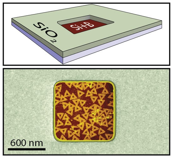
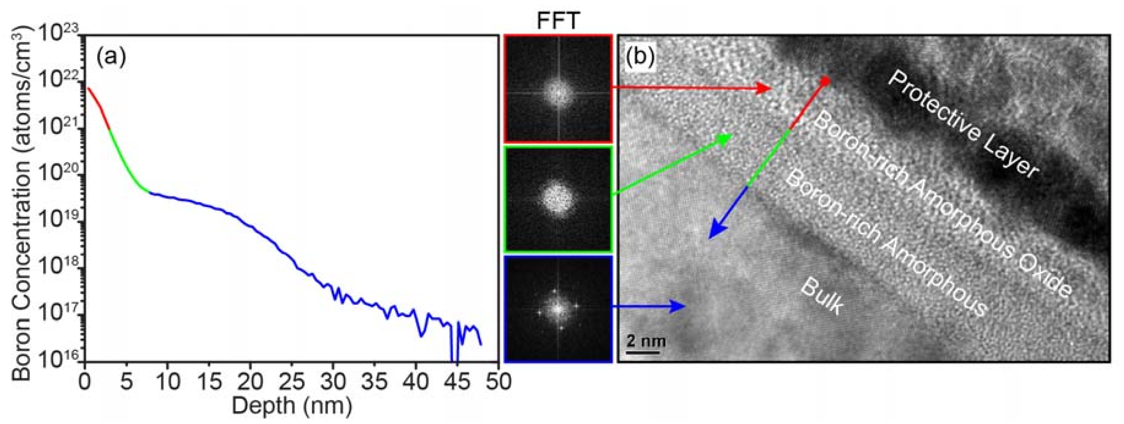
2. Results
3. Discussion
4. Materials and Methods
4.1. DNA Origami Synthesis
4.2. Substrate Cleaning
4.3. DNA Origami Deposition
4.4. Determining Surface Density
5. Conclusions
Supplementary Materials
Author Contributions
Funding
Acknowledgments
Conflicts of Interest
Abbreviations
| DNA | deoxyribonucleic acid |
| SiO2 | silicon dioxide |
| MgCl2 | magnesium chloride |
| [MgCl2] | magnesium chloride concentration |
| SADP | self-aligned double patterning |
| SAQP | self-aligned quadruple patterning |
| DSA | directed self-assembly |
| BCP | block copolymers |
| DSA-BCP | block copolymer directed self-assembly |
| APTES | aminopropyltrimethoxysilane |
| HMDS | hexamethyldisilazane |
| SAM | self-assembled monolayer |
| XPS | X-ray Photoelectron Spectroscopy |
| SIMS | Secondary Ion Mass Spectroscopy |
| TEM | Transmission Electron Microscopy |
| FIB | focused-ion beam |
| HF | hydrofluoric acid |
| FFT | Fast Fourier Transform |
| HCl | hydrochloric acid |
| AFM | atomic force microscopy |
| EDTA | ethylenediaminetetraacetic acid |
| FAM | fluorescein amidite |
References
- Moore, G.E. Cramming more components onto integrated circuits. Electronics 1965, 38, 114–117. [Google Scholar] [CrossRef]
- Moore, G.E. Progress in digital integrated electronics. Int. Electron Devices Meet. 1975, 21, 11–13, reprinted in IEEE Solid-State Circuits Soc. Newsl. 2006, 11, 36–37. [Google Scholar] [CrossRef]
- Gallatin, G. Nanofabrication: A perspective from litho practitioners. In Proceedings of the SRC/IBM/ONR Workshop on Bio-Nanofabrication and Materials, San Jose, CA, USA; 16–17 November 2016. [Google Scholar]
- Xu, K.; Souriau, L.; Hellin, D.; Versluijs, J.; Wong, P.; Vangoidsenhoven, D.; Vandenbroeck, N.; Dekkers, H.; Shi, X.; Albert, J.; et al. Key contributors for improvement of line width roughness, line edge roughness, and critical dimension uniformity: 15 nm half-pitch patterning with extreme ultraviolet and self-aligned double patterning. J. Micro Nanolithogr. MEMS MOEMS 2013, 12, 041302. [Google Scholar] [CrossRef]
- Kodama, C.; Ichikawa, H.; Nakayama, K.; Nakajima, F.; Nojima, S.; Kotani, T.; Ihara, T.; Takahashi, A. Self-Aligned Double and Quadruple Patterning Aware Grid Routing Methods. IEEE Trans. Comput. Des. Integr. Circuits Syst. 2015, 34, 753–765. [Google Scholar] [CrossRef]
- Wu, B.; Kumar, A. Extreme Ultraviolet Lithography; McGraw-Hill: New York, NY, USA, 2009; pp. 12–34. ISBN 9780071549189. [Google Scholar]
- Mimotogi, S. Extension of patterning technologies down to sub-10nm half pitch. Proc. SPIE 2013, 8685, 868503–868509. [Google Scholar]
- SemiSynBio Consortium and Roadmap Development. Available online: https://www.src.org/program/grc/semisynbio/semisynbio-consortium-roadmap/ (accessed on 28 July 2017).
- International Technology Roadmap for Semiconductors 2.0 2015 Edition. Available online: http://www.itrs2.net/itrs-reports.html (accessed on 20 October 2017).
- Quader, K.N. Flash Memory at a Cross-Road: Challenges and Opportunities. In Proceedings of the 2012 4th IEEE International Memory Workshop, Milan, Italy, 20 March 2012; IEEE: Piscataway, NJ, USA, 2012; pp. 1–4. [Google Scholar]
- Edwards, E.W.; Müller, M.; Stoykovich, M.P.; Solak, H.H.; de Pablo, J.J.; Nealey, P.F. Dimensions and Shapes of Block Copolymer Domains Assembled on Lithographically Defined Chemically Patterned Substrates. Macromolecules 2007, 40, 90–96. [Google Scholar] [CrossRef]
- Seeman, N.C. DNA in a material world. Nature 2003, 421, 427–431. [Google Scholar] [CrossRef] [PubMed]
- Deng, Z.; Mao, C. Molecular Lithography with DNA Nanostructures. Angew. Chem. Int. Ed. 2004, 43, 4068–4070. [Google Scholar] [CrossRef] [PubMed]
- He, Y.; Ye, T.; Ribbe, A.E.; Mao, C. DNA-Templated Fabrication of Two-Dimensional Metallic Nanostructures by Thermal Evaporation Coating. J. Am. Chem. Soc. 2011, 133, 1742–1744. [Google Scholar] [CrossRef] [PubMed]
- Ma, X.; Huh, J.; Park, W.; Lee, L.P.; Kwon, Y.J.; Sim, S.J. Gold nanocrystals with DNA-directed morphologies. Nat. Commun. 2016, 7, 12873. [Google Scholar] [CrossRef] [PubMed] [Green Version]
- Bates, F.S.; Fredrickson, G.H. Block Copolymer Thermodynamics: Theory and Experiment. Annu. Rev. Phys. Chem. 1990, 41, 525–557. [Google Scholar] [CrossRef] [PubMed]
- Diagne, C.T.; Brun, C.; Gasparutto, D.; Baillin, X.; Tiron, R. DNA Origami Mask for Sub-Ten-Nanometer Lithography. ACS Nano 2016, 10, 6458–6463. [Google Scholar] [CrossRef] [PubMed]
- Surwade, S.P.; Zhou, F.; Wei, B.; Sun, W.; Powell, A.; O’Donnell, C.; Yin, P.; Liu, H. Nanoscale Growth and Patterning of Inorganic Oxides Using DNA Nanostructure Templates. J. Am. Chem. Soc. 2013, 135, 6778–6781. [Google Scholar] [CrossRef] [PubMed]
- Shen, B.; Linko, V.; Tapio, K.; Kostiainen, M.A.; Toppari, J.J. Custom-shaped metal nanostructures based on DNA origami silhouettes. Nanoscale 2015, 7, 11267–11272. [Google Scholar] [CrossRef] [PubMed] [Green Version]
- Zhou, F.; Sun, W.; Ricardo, K.B.; Wang, D.; Shen, J.; Yin, P.; Liu, H. Programmably Shaped Carbon Nanostructure from Shape-Conserving Carbonization of DNA. ACS Nano 2016, 10, 3069–3077. [Google Scholar] [CrossRef] [PubMed]
- Ke, Y.; Ong, L.L.; Shih, W.M.; Yin, P. Three-Dimensional Structures Self-Assembled from DNA Bricks. Science. 2012, 338, 1177–1183. [Google Scholar] [CrossRef] [PubMed] [Green Version]
- Mandelkern, M.; Elias, J.G.; Eden, D.; Crothers, D.M. The dimensions of DNA in solution. J. Mol. Biol. 1981, 152, 153–161. [Google Scholar] [CrossRef]
- Green, C.M.; Schutt, K.; Morris, N.; Zadegan, R.M.; Hughes, W.L.; Kuang, W.; Graugnard, E. Metrology of DNA arrays by super-resolution microscopy. Nanoscale 2017, 9, 10205–10211. [Google Scholar] [CrossRef] [PubMed]
- Rothemund, P.W.K. Folding DNA to create nanoscale shapes and patterns. Nature 2006, 440, 297–302. [Google Scholar] [CrossRef] [PubMed] [Green Version]
- Scheible, M.B.; Ong, L.L.; Woehrstein, J.B.; Jungmann, R.; Yin, P.; Simmel, F.C. A Compact DNA Cube with Side Length 10 nm. Small 2015, 11, 5200–5205. [Google Scholar] [CrossRef] [PubMed] [Green Version]
- Jin, Z.; Sun, W.; Ke, Y.; Shih, C.-J.; Paulus, G.L.C.; Hua Wang, Q.; Mu, B.; Yin, P.; Strano, M.S. Metallized DNA nanolithography for encoding and transferring spatial information for graphene patterning. Nat. Commun. 2013, 4, 1663. [Google Scholar] [CrossRef] [PubMed] [Green Version]
- Surwade, S.P.; Zhao, S.; Liu, H. Molecular Lithography through DNA-Mediated Etching and Masking of SiO2. J. Am. Chem. Soc. 2011, 133, 11868–11871. [Google Scholar] [CrossRef] [PubMed]
- Zhou, F.; Michael, B.; Surwade, S.P.; Ricardo, K.B.; Zhao, S.; Liu, H. Mechanistic Study of the Nanoscale Negative-Tone Pattern Transfer from DNA Nanostructures to SiO2. Chem. Mater. 2015, 27, 1692–1698. [Google Scholar] [CrossRef]
- Sarveswaran, K.; Gao, B.; Kim, K.N.; Bernstein, G.H.; Lieberman, M. Adhesion of DNA nanostructures and DNA origami to lithographically patterned self-assembled monolayers on Si[100]. In Alternative Lithographic Technologies II; Herr, D.J.C., Ed.; International Society for Optics and Photonics: Bellingham, WA, USA, 2010; p. 76370M. [Google Scholar]
- Gopinath, A.; Rothemund, P.W.K. Optimized Assembly and Covalent Coupling of Single-Molecule DNA Origami Nanoarrays. ACS Nano 2014, 8, 12030–12040. [Google Scholar] [CrossRef] [PubMed]
- Love, J.C.; Estroff, L.A.; Kriebel, J.K.; Nuzzo, R.G.; Whitesides, G.M. Self-Assembled Monolayers of Thiolates on Metals as a Form of Nanotechnology. Chem. Rev. 2005, 105, 1103–1170. [Google Scholar] [CrossRef] [PubMed]
- Kershner, R.J.; Bozano, L.D.; Micheel, C.M.; Hung, A.M.; Fornof, A.R.; Cha, J.N.; Rettner, C.T.; Bersani, M.; Frommer, J.; Rothemund, P.W.K.; et al. Placement and orientation of individual DNA shapes on lithographically patterned surfaces. Nat. Nanotechnol. 2009, 4, 557–561. [Google Scholar] [CrossRef] [PubMed] [Green Version]
- Tanaka, S.; Taniguchi, M.; Kawai, T. Selective Adsorption of DNA onto SiO2 Surface in SiO2/SiH Pattern. Jpn. J. Appl. Phys. 2004, 43, 7346–7349. [Google Scholar] [CrossRef]
- Amodio, A.; Adedeji, A.F.; Castronovo, M.; Franco, E.; Ricci, F. pH-Controlled Assembly of DNA Tiles. J. Am. Chem. Soc. 2016, 138, 12735–12738. [Google Scholar] [CrossRef] [PubMed]
- Billingsley, D.J.; Lee, A.J.; Johansson, N.A.B.; Walton, A.; Stanger, L.; Crampton, N.; Bonass, W.A.; Thomson, N.H. Patchiness of ion-exchanged mica revealed by DNA binding dynamics at short length scales. Nanotechnology 2014, 25, 025704. [Google Scholar] [CrossRef] [PubMed]
- Whittle, K.M.; Vick, G.L. Control of Boron Diffusion from a Pyrolitic Borosilicate Glass Source. J. Electrochem. Soc. 1969, 116, 645–648. [Google Scholar] [CrossRef]
- Sadigh, B.; Lenosky, T.J.; Caturla, M.-J.; Quong, A.A.; Benedict, L.X.; Diaz de la Rubia, T.; Giles, M.M.; Foad, M.; Spataru, C.D.; Louie, S.G. Large enhancement of boron solubility in silicon due to biaxial stress. Appl. Phys. Lett. 2002, 80, 4738–4740. [Google Scholar] [CrossRef]
- Vick, G.L.; Whittle, K.M. Solid Solubility and Diffusion Coefficients of Boron in Silicon. J. Electrochem. Soc. 1969, 116, 1142–1144. [Google Scholar] [CrossRef]
- Brown, D.M.; Kennicott, P.R. Glass Source Diffusion in Si and SiO2. J. Electrochem. Soc. 1971, 118, 293–300. [Google Scholar] [CrossRef]
- Busen, K.M.; FitzGibbons, W.A.; Tsang, W.K. Ellipsometric Investigations of Boron-Rich Layers on Silicon. J. Electrochem. Soc. 1968, 115, 291–294. [Google Scholar] [CrossRef]
- Tenney, A.S.; Ghezzo, M. Etch Rates of Doped Oxides in Solutions of Buffered HF. J. Electrochem. Soc. 1973, 120, 1091–1095. [Google Scholar] [CrossRef]
- Fujii, M.; Sugimoto, H.; Hasegawa, M.; Imakita, K. Silicon nanocrystals with high boron and phosphorus concentration hydrophilic shell—Raman scattering and X-ray photoelectron spectroscopic studies. J. Appl. Phys. 2014, 115, 084301. [Google Scholar] [CrossRef]
- Zhang, X.G. Electrochemistry of Silicon and Its Oxide; Kluwer Academic/Plenum Publishers: New York, NY, USA, 2001; pp. 45–89. ISBN 0-306-46541-8. [Google Scholar]
- DeWalt-Kerian, E.L.; Kim, S.; Azam, M.S.; Zeng, H.; Liu, Q.; Gibbs, J.M. pH-Dependent Inversion of Hofmeister Trends in the Water Structure of the Electrical Double Layer. J. Phys. Chem. Lett. 2017, 8, 2855–2861. [Google Scholar] [CrossRef] [PubMed]
- Besra, L.; Liu, M. A review on fundamentals and applications of electrophoretic deposition (EPD). Prog. Mater. Sci. 2007, 52, 1–61. [Google Scholar] [CrossRef]
- Boström, M.; Deniz, V.; Franks, G.V.; Ninham, B.W. Extended DLVO theory: Electrostatic and non-electrostatic forces in oxide suspensions. Adv. Colloid Interface Sci. 2006, 123, 5–15. [Google Scholar] [CrossRef] [PubMed]
- Ong, S.; Zhao, X.; Eisenthal, K.B. Polarization of water molecules at a charged interface: Second harmonic studies of the silica/water interface. Chem. Phys. Lett. 1992, 191, 327–335. [Google Scholar] [CrossRef]
- Zhirnov, V.; Zadegan, R.M.; Sandhu, G.S.; Church, G.M.; Hughes, W.L. Nucleic acid memory. Nat. Mater. 2016, 15, 366–370. [Google Scholar] [CrossRef] [PubMed]
- Lin, C.; Perrault, S.D.; Kwak, M.; Graf, F.; Shih, W.M. Purification of DNA-origami nanostructures by rate-zonal centrifugation. Nucleic Acids Res. 2013, 41, e40. [Google Scholar] [CrossRef] [PubMed]
- Aghebat Rafat, A.; Pirzer, T.; Scheible, M.B.; Kostina, A.; Simmel, F.C. Surface-assisted large-scale ordering of DNA origami tiles. Angew. Chem. Int. Ed. Engl. 2014, 53, 7665–7668. [Google Scholar] [CrossRef] [PubMed]
- Kocabey, S.; Kempter, S.; List, J.; Xing, Y.; Bae, W.; Schiffels, D.; Shih, W.M.; Simmel, F.C.; Liedl, T. Membrane-Assisted Growth of DNA Origami Nanostructure Arrays. ACS Nano 2015, 9, 3530–3539. [Google Scholar] [CrossRef] [PubMed]
- Woo, S.; Rothemund, P.W.K. Self-assembly of two-dimensional DNA origami lattices using cation-controlled surface diffusion. Nat. Commun. 2014, 5, 4889. [Google Scholar] [CrossRef] [PubMed] [Green Version]


© 2018 by the authors. Licensee MDPI, Basel, Switzerland. This article is an open access article distributed under the terms and conditions of the Creative Commons Attribution (CC BY) license (http://creativecommons.org/licenses/by/4.0/).
Share and Cite
Takabayashi, S.; Kotani, S.; Flores-Estrada, J.; Spears, E.; Padilla, J.E.; Godwin, L.C.; Graugnard, E.; Kuang, W.; Sills, S.; Hughes, W.L. Boron-Implanted Silicon Substrates for Physical Adsorption of DNA Origami. Int. J. Mol. Sci. 2018, 19, 2513. https://doi.org/10.3390/ijms19092513
Takabayashi S, Kotani S, Flores-Estrada J, Spears E, Padilla JE, Godwin LC, Graugnard E, Kuang W, Sills S, Hughes WL. Boron-Implanted Silicon Substrates for Physical Adsorption of DNA Origami. International Journal of Molecular Sciences. 2018; 19(9):2513. https://doi.org/10.3390/ijms19092513
Chicago/Turabian StyleTakabayashi, Sadao, Shohei Kotani, Juan Flores-Estrada, Elijah Spears, Jennifer E. Padilla, Lizandra C. Godwin, Elton Graugnard, Wan Kuang, Scott Sills, and William L. Hughes. 2018. "Boron-Implanted Silicon Substrates for Physical Adsorption of DNA Origami" International Journal of Molecular Sciences 19, no. 9: 2513. https://doi.org/10.3390/ijms19092513