1. Introduction
SPR is one of the most powerful analytical methods for evaluating biomolecular interactions in real-time without the need for labeling. Using SPR, it is possible to measure changes in refractive index on the small and thin area of the sensor chip surface. Because of these benefits, SPR sensors have been widely used for detecting various chemical and biological compounds in the laboratory in the fields of environmental analysis [
1], food safety [
2], and clinical diagnostics [
3].
It is noteworthy that the use of SPR sensor systems has been undergoing a change. For example, in novel drug projects in the field of pharmaceutical biotechnology, a compact desktop type SPR sensor system with a higher throughput would be desirable [
4]. Also, in the field of social healthcare, as a safety countermeasure for the spreading of infection diseases, a handheld type SPR sensor system for on-site analysis is urgently needed [
5].
In order to comply with these needs, an SPR sensor system with higher throughput with multi-channel sensing points and a more compact size is desired. In the case of a conventional type SPR sensor system, which is comprised of a Kretschmann configuration system [
6], the optics system of the instrument can be classified into one of three types:
The first type employs a fan shaped mono-chromatic beam as the surface plasmon incident light source with a hemi-circular prism as the surface plasmon coupler [
7]. As a detector in this optic system, a linear CCD sensor or a 2D CCD camera is usually used to measure the intensity of the reflected fan shaped light, including the SPR dip. The SPR sensor response is measured as a change in the SPR dip position. The advantage of this system is that it permits the SPR response to be observed over a wide range of approximately 10 degrees at a time and that it does not contain any moving parts like a motor stage for scanning angles.
The second type uses a particular fixed angle small point mono-chromatic beam as the surface plasmon incident light source with a triangular or a hemi-circular prism as the surface plasmon coupler [
8]. The angle is set near the expected SPR dip. A photodiode is usually used in this system to measure the intensity of the reflected light at the same fixed angle of the incident light. Since the SPR sensor signal is observed as the intensity of the reflected light at the shoulder of the SPR sensor response curve, the sensitivity is higher than that for measuring the change in the SPR dip angle. However, many samples cannot be measured using this system, because the sensing region is only one point. Also, the system needs stages for scanning the dip position of the SPR sensor curve to determine the initial observing angle before the measurement.
The third type is a combination of the optic systems discussed above. An angle scanning mono-chromatic beam is used as an incident light to form a fan-like shaped beam. The incident light is achieved using a galvanometer based optical scanner, or by moving the position of the beam along the center of the sensing point of the prism surface using a rotary stage [
9]. To measure the intensity of the reflected light along the scanning angle, a photodiode which is able to cover the angle range of the reflected light or a 2D CCD camera is usually used as the detector. The SPR sensor signal response is measured as the change in the SPR dip position because the system is able to observe SPR sensor curve.
In general, these SPR optical configurations have a point or a line shaped sensing region that is approximately 10 to 20 mm in length and 100 μm wide on a sensor chip. In order to achieve a higher throughput measurement system, it is necessary to have a number of flow channels so that multiple samples can be measured simultaneously, and a high speed sample changing fluid system. However, the number of flow cell channels that can be placed on the sensing region for multi-sensing are limited to 20 channels because a flow cell cannot be placed in narrow line shaped sensing region.
On the other hand, another approach to resolving these issues is an SPR imaging system [
10–
15]. The system was designed to observe a certain area on the sensor chip. The size of the sensing area is approximately 20 mm square. To simultaneously measure a number of samples, the sample cell size is usually set to a square with sides of approximately 100 μm in the sensing area. However, there are difficulties associated with the fabrication of such microscopic cells. Therefore, additional sensor chip preparation equipment, like a material spotting inkjet printer, is needed for setting different kinds of samples on microscopic cells. A large circular collimated light is also required to irradiate the wide sensing area on the prism. For that purpose, a beam expander is usually used to reshape the small beam spot size of the laser diode into a large collimated light. The optical pathlength of the system become long. The system needs a more expensive high resolution format CCD camera compared to other SPR systems.
These conventional SPR systems are almost desktop in size. Considering the fact that they are used for on-site analysis, they may not be suitable, because of the size, weight and cost of the instrumentation.
In previous studies, we reported on the development of portable SPR sensor optics and sensor chips with dual- [
16,
17] or multi- [
18] detection points, which are very compact in size relative to the optics and sensor chips. They showed good sensitivity as conventional desktop type SPR sensor systems.
In this study, we wish to report on the development of a novel two dimensional SPR sensor system with a nine point sensing region on the sensor chip at intervals of ca. 5 mm in a reticular pattern. A multiplied beam splitting optics for achieving multi-point sensing was newly designed and fabricated. The system has a scalable optical configuration, which permits the number of sensing points to be increased, with no lens. Therefore, the system is applicable to on-site analysis applications mentioned above.
2. Experimental Section
2.1. Materials and Reagents
Polydimethylsiloxane (PDMS) prepolymer (Sylpot 184), and its curing agent were obtained from Dow Corning Toray Co., Ltd. (Tokyo, Japan). Sucrose was obtained from Wako Pure Chemical Industries, Ltd. (Osaka, Japan). All dilution steps were performed with Millipore filtered water from a Milli-Q system (Nihon Millipore, Tokyo, Japan).
2.2. Fabrication and Principle of the Multiple Beam Splitter Light Source
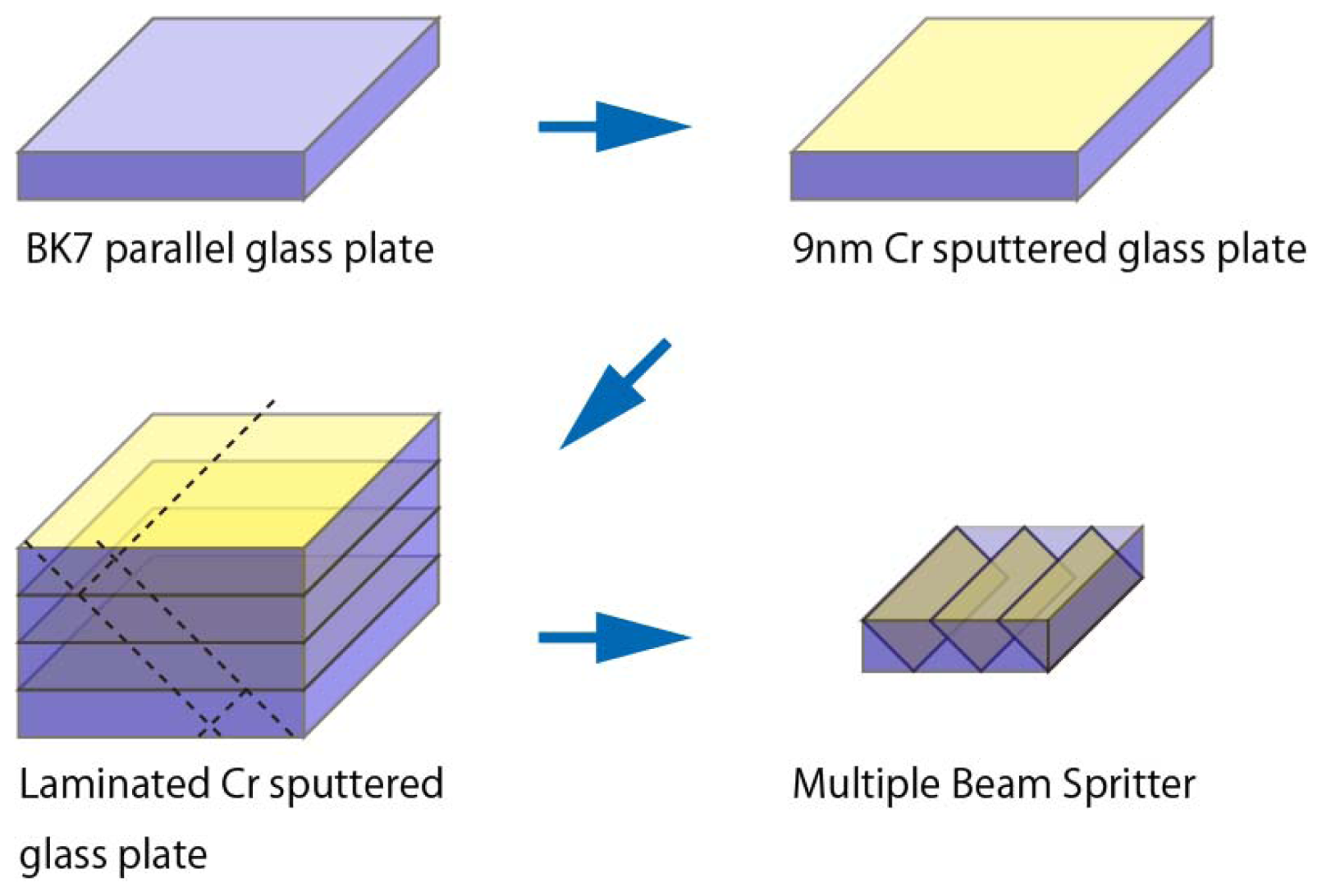
Figure 1 shows the method used in the fabrication of the Multiple Beam Splitter Optics used in this study. First, as a reflection film of the beam splitter, thin metal chromium was deposited on a BK7 parallel glass plate (12 (width) × 18 (height) × 5 (thickness) mm, KADOMI Optical Industry, Tokyo, Japan) with a thickness of
ca. 9 nm using sputtering equipment (M92-0007, SEED Lab. Co., Kanagawa, Japan). The three sputtered glass plates were then laminated horizontally using a UV optical adhesive (PHOTOBOND 400, Sunrise MSI Co., Osaka, Japan), so that each of the three reflection film planes were parallel. The block of a laminated beam splitter glass plate was formed into a size of 12 (Width) × 18 (Height) × 5 (thickness) mm, and the reflection angle of film plane was maintained at 45 degrees to the beam entrance surface.
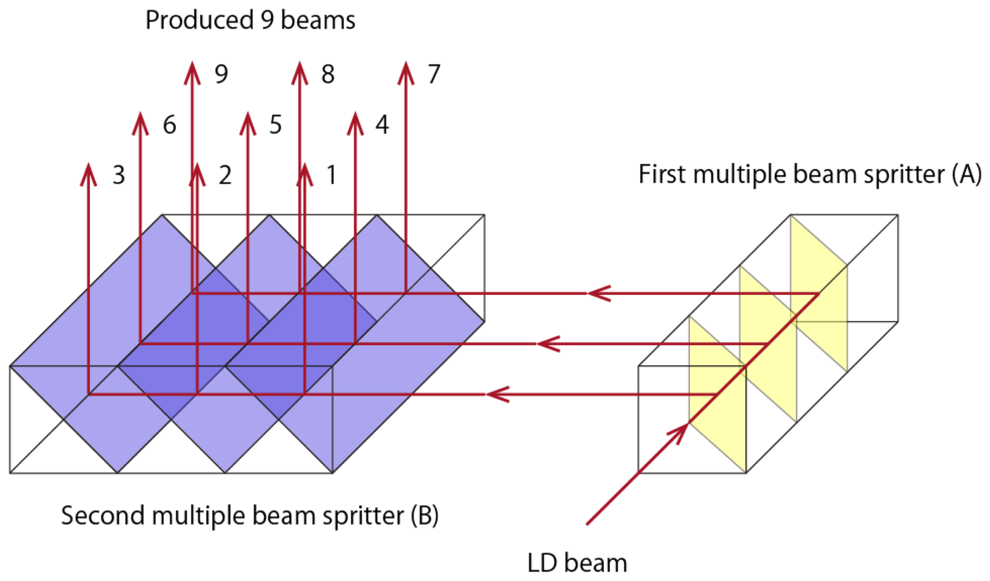
Figure 2 shows the perspective diagram of the direction of radiation of the laser beam. A laser diode module (655 nm, 350 μW, LV-S41, KEYENCE, Osaka, Japan) was used as the light source. In order to transform one beam to nine beams, two multiple beam splitters were arranged in rows and columns. At the first multiple beam splitter, denoted as A in
Figure 2, a laser beam light source was entered and transformed into the three beams on the three reflecting films. Each divided parallel light beam was irradiated onto the second multiple beam splitters, denoted as B in
Figure 2. As a result, nine, two dimensional, parallel light beams were observed at the exit of the second multiple beam splitters. Each of the nine beams was assigned a number for convenience as shown in
Figure 2. The intervals of the nine beams were 5 mm each and the shape of the beams was the same. The power of each beam was measured using a handy laser power meter (7Z01560, Ophir Optronics Solutions Ltd., Jerusalem, Israel). The calculated reflectivity, transparency and absorption factor of P-polarized and S-Polarized light using the optical design software, ZEMAX (Radiant Zemax LLC, Redmond, WA, USA) is shown in
Table 1.
Table 2 shows the calculated power of the nine beams with the optical factor in
Table 1. The normalized observed power of each beam was correlated well with the calculated powers.
2.3. Optical System of 2D SPR Sensor
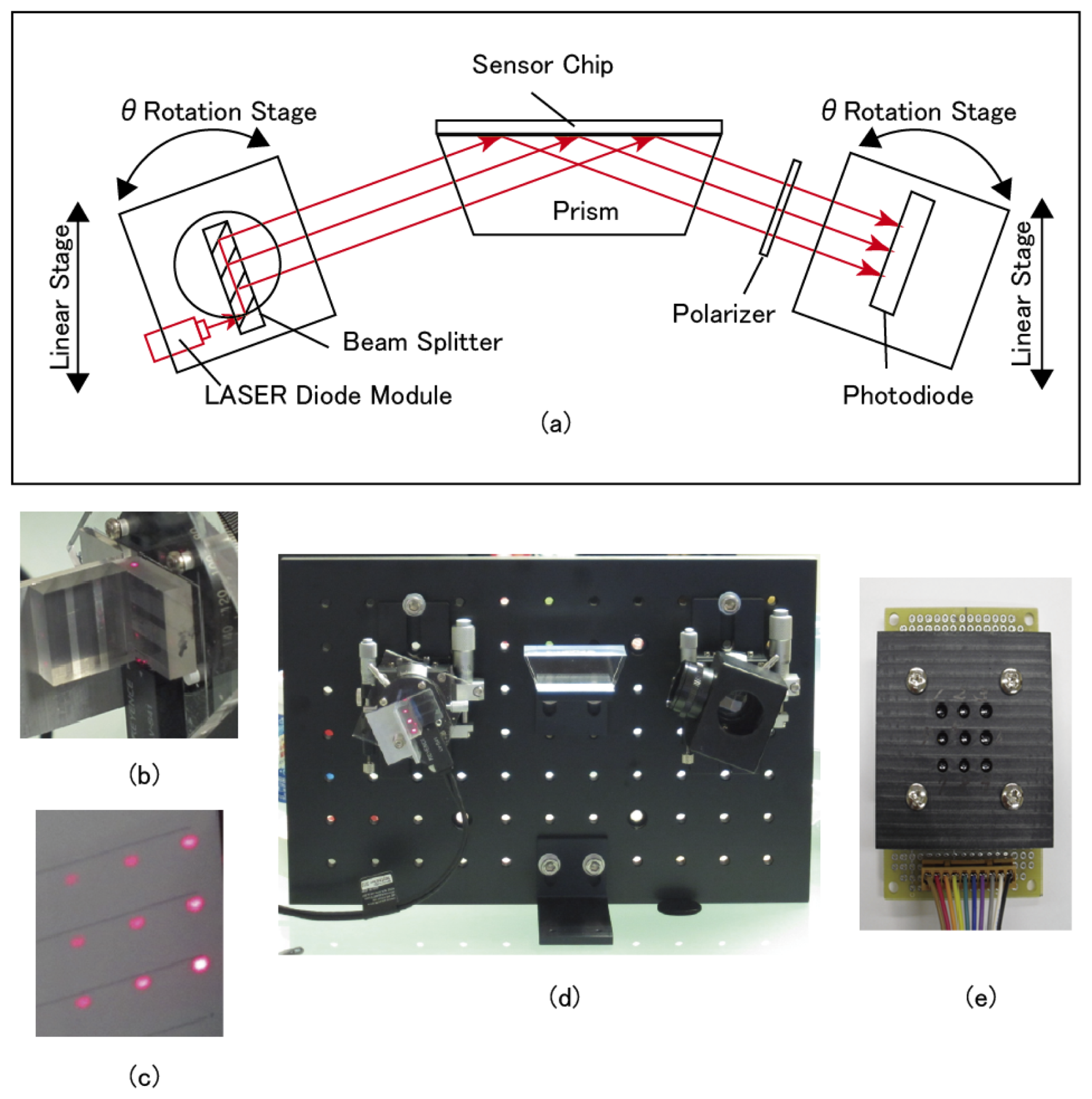
Figure 3 shows the optical system for the 2D SPR sensor developed in this study. The configuration of the optical system and the theory of its operation were based on the principle of a conventional fixed angle light intensity type SPR sensor system, except for the multiple beam splitter light source.
The optical system was constructed on an aluminum optical base plate (BBA6-200-300, 300 mm in width × 200 mm in height, MISUMI Corporation, Tokyo, Japan). The light source, the multiplied nine laser beams optic, was set on a rotary stage (RPG38, MISUMI Corporation) as the θ-Axis transfer and a linear stage (XCRS40, MISUMI Corporation) as the Y-Axis transfer. The detector consisted of a polarizer (NT47-315, Edmund Optics Inc., Barrington, NJ, USA) and nine photodiodes (SP-1CL3, KODENSHI CORP., Kyoto, Japan) set in a lattice pattern. The lattice pattern interval is the same as the multiplied nine laser beams. These were set on a rotary stage (RPG38, MISUMI Corporation) as the θ-Axis transfer and a linear stage (XCRS40, MISUMI Corporation) as the Y-Axis transfer. A trapezoidal prism (BK7, 54 mm (upper side) × 39.7 mm (lower side) × 18.7 mm (height) × 30 mm (width), 69° base angle, KADOMI Optical Industry, Tokyo, Japan) was centrally located between the light source and the detector. An optically parallel glass plate (BK7, surface flatness of 2λ, parallelism of 60″, 54 mm distance × 30 mm width × 0.5 mm thickness), sputtered with a 3 nm layer of titanium and a 45 nm layer of gold using sputtering equipment (M92-0007, SEED Lab. Co., Kanagawa, Japan), was used as the SPR sensor chip. The Au sensor chip was optically integrated with the trapezoidal prism surface using matching oil (nD = 1.5150 ± 0.0002, Type A, Catalog No. 16482, Cargille Laboratories Inc., Cedar Grove, NJ, USA).
The light beams from the multiple beam splitter optics entered the trapezoidal prism directly. The center beam of the nine beams was set to the center of the surface of the Au sensor chip. The reflected light beams were then passed through the polarizer to eliminate s-polarized light. The detector was set so that the each beam reached the corresponding photodiode element respectively.
The working distance between the center of the prism and the center of light beam source was 94 mm at 70 degrees of incident light. The p-polarized light of the reflected light corresponding to the SPR was measured under dark room conditions. The signal of the SPR sensor was obtained by subtracting the dark current signal from the observed signal. The photocurrent from each photodiode was converted to voltage by current to voltage circuit (
Figure 4). The each voltage was recorded using 34970A Data Acquisition/Data Logger Switch Unit (Agilent, Loveland, CO, USA) with a 20 Channel Multiplexer Module 34901A (Agilent) and a BenchLink Data Logger software (Agilent).
2.4. Fabrication of the Sensor Chip Fluidics
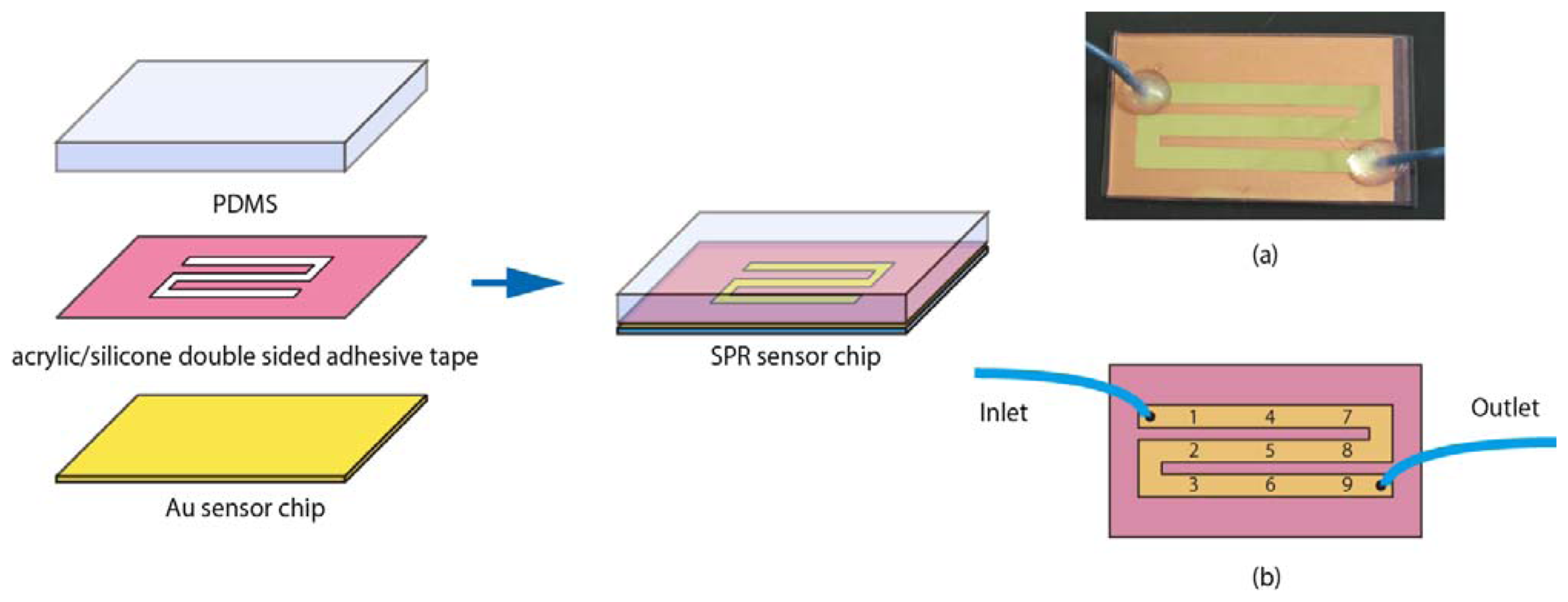
First, as shown in
Figure 5, an A4 formatted sheet of acrylic/silicone double sided adhesive tape obtained from Sumitomo 3M Limited Company (No. 4357, Tokyo, Japan) was cut out to form a flow cell. The flow channel size was 4 mm in width, 136 mm in length with a thickness of 0.1mm. The flow channel sheet was then set on the Au sensor chip with the adhesive. The Au sensor chip with the flow channel was covered with a PDMS plate (54 mm width × 30 mm distance, thickness of 5 mm) with two 1.5 mm diameter holes as an inlet and an outlet port. Finally, two PEEK tubes (I.D. 0.25 mm, O.D. 1/16 inches) were connected into inlet and outlet port using adhesive (SuperX No. 8008, CEMEDINE CO. LTD., Tokyo, Japan) for sending the sample solutions. The volume of the flow cell was 54.4 μL.
2.5. Flow Analysis System Using 2D SPR Sensor
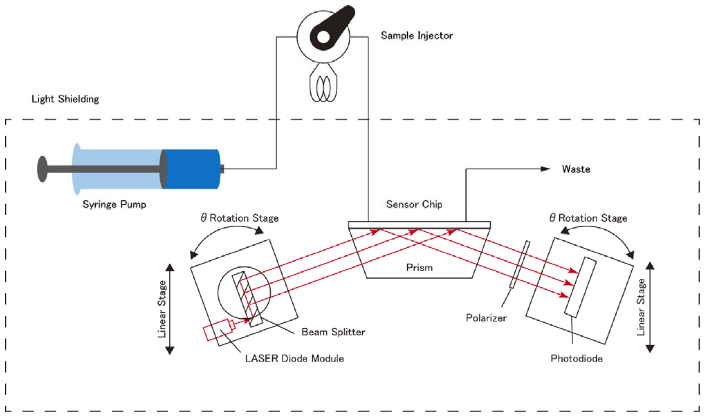
Figure 6 shows the 2D SPR Sensor system. The system consisted of a syringe pump (PHD 2000 Infusion 70-2000, Harvard Apparatus, Holliston, MA, USA), a sample injector (VI-11, FLOM Co. Ltd., Tokyo, Japan) with a sample loop of 150 μL, the sensor chip, and the developed 2D SPR sensor.
4. Conclusions/Outlook
The optical system developed in this study is superior to other systems in scalability because it is comprised of a simple optical configuration without a lens. The size of all of the optical elements from the light source to the prism and detector can be readily changed by scaling-up or scaling-down. This feature can be realized by changing the size of the trapezoidal prism for sample installation, the number of multiplied laser beams, the thickness of sputtered chromium for the light intensity of each beam, the intervals of the beams and the number of detectors.
When the optical elements are miniaturized, it becomes possible to manufacture a palm-sized multichannel SPR system using micro-sample cells. When the optical elements are enlarged, a SPR system using a 96-well microtiter plate as a measurement cell can be manufactured. Since no lens is used in this SPR sensor system for the convergence of light paths, the manufacturing costs can be expected to be modest and the size of the system would be compact compared to the conventional systems used currently.
